One puzzle about this charger is it's unclear who makes it and what model it is. The case says it's the KMS AC-09 but the circuit board says "TC09-new-V4.2". Amazon lists the brand as "Cosmos®", but I couldn't find any sign that KMS or Cosmos are actual companies. After some web searches, I think the charger is built by Guangzhou Panyu Qiaonan Saidi Electronic Factory (more) as the TC09 charger for $5.30 wholesale, or maybe HK Yingjia International, a consumer electronics manufacturer in Shenzhen (more). In any case, I'll call this the "KMS charger" since I need to call it something.
In my previous lab analysis of 12 chargers, I compared a dozen different chargers in 9 different categories, rating them from 1 to 5 'bolts' and the KMS charger came in about average in terms of performance. The results for the KMS charger are summarized below. For details on these measurements, see my previous article A dozen USB chargers in the lab).
| Overall rating |  |
|---|---|
| Vampire (idle) power usage |  |
| Efficiency under load |  |
| Achieves power rating |  |
| Spikes in output |  |
| High-frequency noise in output |  |
| Ripple in output |  |
| Voltage sag |  |
| Current sag |  |
| Regulation quality |  |
The good and the bad
Overall, this charger is much higher quality than the $2 counterfeit chargers, but considerably lower quality than name-brand chargers.The charger provides more filtering than basic chargers, from the large input choke to the multiple output inductors. It includes X and Y capacitors for filtering.
The charger looks mostly safe, although it doesn't have UL certification and I suspect it would fail certification. The 6mm clearance between the primary and secondary looks solid. However, the transformer windings are only separated by 3mm, rather than 6mm, as I show below. (This is still much superior to the $2 chargers that have almost no separation.)
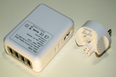
One interesting feature of the power supply is the power plug can be interchanged for use in different countries. (Some other chargers such as the HP TouchPad and Apple iPad are similar.)
The charger has some quality issues. The power quality measurements I did in my previous article show the KMS charger has fairly poor quality output, with a lot of noise in the output.
The IC datasheet recommends 200 mm2 of foil on the IC output pins to provide cooling. I measured about 18 mm2 (less than 10% of recommended), which suggests the charger may overheat under full load.
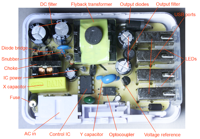
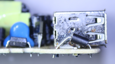
The above photo shows that the build quality of the charger is not extremely high. The inductor at the front right is very crooked, and the optocoupler at the left is somewhat crooked. While this doesn't affect the performance, it shows the assembly was rapid rather than careful. More concerning, some of the solder joints appear to be almost bridged, which could cause catastrophic failure of the charger. I also found a government report of a KMS charger catching fire, apparently due to a loose wire in the power plug.
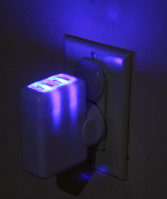
One unique feature of the charger is the blue LEDs which cause it to emit an eerie blue glow when in use. A lot of users dislike this though (according to reviews), because the light is distracting at night.
The circuit
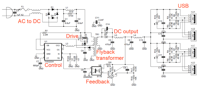
For readers interested in circuits, I have prepared the above approximate schematic (click for a larger view). The circuit is pretty straightforward compared to other chargers (look at my iPhone charger schematic for comparison). Starting at the upper left, the input AC is converted to DC by the diode bridge, and then filtered by a simple inductor-capacitor filter. This high-voltage DC is connected to the flyback transformer primary. The THX203H control IC switches the other side of the flyback transformer to ground through the current-sense resistors R12A and R12B and inductor L3. (Most chargers use a separate switching transistor, but in this charger, the transistor is inside the control IC.) The snubber circuit R2, C3, and D6 absorbs some of the high-frequency switching spikes (although looking at the output below, this circuit isn't entirely successful). The auxiliary transformer winding and D7 and C4 provide the DC power to the control IC. The optocoupler provides feedback to the IC, indicating the output voltage level.
On the secondary side, the high-speed Schottky diodes (D5) convert the transformer output to DC. This is then filtered through an inductor-capacitor filter that smooths it out. The output voltage feedback is generated by the TL431A regulator and fed into the optocoupler.[1]
Finally, the actual USB output circuitry has more components than you'd expect. For each pair of ports, four resistors set the D+ and D- voltages to indicate to devices that the charger is (pretending to be) an Apple 2A charger. Each port has a small bypass capacitor to smooth out power transients. Finally there are two blue LEDs with current-limiting resistors to provide the blue glow.
The controller IC poses a bit of a mystery. It's labeled as the THX 203H controller, which turns out to be manufactured by NanJing TongHuaXin Electronic Co, Ltd., a Chinese switching power supply chip company (details). The datasheet for this part is very hard to understand, as it is machine-translated from Chinese, for example:
The startup circuit inside IC is designed as a particular current inhalation way, so it can start up with the magnification function of the power switch tube itself.After some more investigation, this chip seems to be the SDC603 Current Mode PWM Controller designed by SDC Semi (Shaoxing Devechip Microelectronics Co., Ltd.). This is a Chinese state-level R&D center that is part of China's Torch Plan Project to develop high-tech industries. (Also check out the SDC company song.)
The controller chip is a basic 8-pin current-mode PWM controller chip. It includes a built-in NPN power transistor, which reduces the charger part count. The chip can produce 12 watts output power.
Circuit board
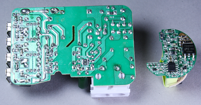
The above picture shows the KMS charger circuit board on the left and a circuit board from the HP TouchPad charger on the right. Compact phone chargers such as the iPhone or TouchPad chargers go to amazing effort to pack the components as tightly as possible. The KMS charger on the other hand has a much more spacious design with a lot of wasted space. Since any charger with 4 USB ports is going to be fairly large, they probably figured it's not worth the effort to make the rest of the circuitry compact. The difference in density between the two circuit boards is striking, though.
A key safety feature of the KMS charger is visible in the middle of the circuit board - note the angular cut-out slot, and the empty vertical region with no circuitry. This isolates the high-voltage circuits on the right from the low-voltage output circuits on the left. The KMS charger has a safe 6mm gap and the cut-out provides additional creepage distance. Counterfeit chargers usually skip this critical safety feature, with only a millimeter or two keeping the high voltage from reaching the output and shocking the user.
You might wonder how the charger works if the high voltage and low voltage circuits are separated by a gap. The key is that any components that cross this gap must be specially designed to avoid electrical hazards. The key component is the flyback transformer, which transfers the power through magnetic fields, avoiding any direct electrical connection between the two sides. The feedback signal passes from the secondary to the primary through an optocoupler, which transmits the feedback through a light signal, again avoiding an electrical connection. Finally, a Y safety capacitor connects the primary and secondary grounds to reduce electrical noise. The design of a Y capacitor ensures it won't pass dangerous electrical currents, and won't short out even under fault conditions.
Transformer teardown
The flyback transformer is the key component of a charger and usually the largest and most expensive. The transformer is where the high input voltage is converted to the output voltage, and the two voltages are in extremely close proximity, so the safety of the transformer is critical. From the outside, you can't tell if the manufacturer saved a few cents by leaving out most of the insulation, as happens with $2 chargers. I tore apart the transformer of the KMS charger to see what's inside.The black circle on top of the transformer seen earlier is simply a foam disk, which helps reduce transformer noise by padding the transformer against the case. If a charger makes a high-pitched noise, it's usually coming from the transformer. Power supplies are usually designed with switching frequencies higher than people can hear, but in some circumstances it's still audible, especially if you are young and haven't lost high frequency hearing.
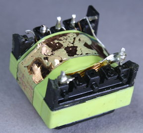
Under the first layers of insulating tape is a copper 'belly band' which surrounds the transformer to provide noise shielding from eddy currents in the transformer.[2] This copper shielding is omitted from super-cheap transformers, showing that this charger goes beyond the minimum.
The windings are all separated by insulating tape. Under the belly band and insulating tape is the auxiliary winding, which provides power to the control IC. You might wonder why the IC needs a separate power supply instead of using the USB power output, but this wouldn't be safe because the USB output would no longer be isolated from the input. This winding is 9 turns of wire; since the IC requires low current, the wire is fairly thin.
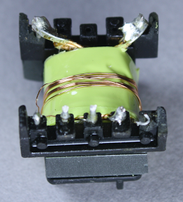
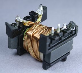
Above you can see half of the primary winding, which is fed by the input power. This winding has 40 turns of wire.
An interesting safety feature is the 3 mm "margin tape"[3] to the lower right of the winding, which ensures that the primary winding stays 3 mm away from the edge. I was interested to see this, since other transformers I've disassembled use triple-insulated wire instead of boundary tape. To ensure safe electrical isolation between the primary and secondary windings, either the secondary wires need to be triple-insulated, or there needs to be at least 6mm of distance between the windings. Super-small chargers don't have 3mm of extra room, so they use the more expensive triple-insulated wire. But since the KMS is larger, it uses the 3mm margin tape. I'm not an expert on safety requirements, but it looks like this transformer doesn't quite meet the requirements. Normally, the margin tape is put on both sides, so there's a total of 6mm creepage distance between the windings.[4][5] But since the tape is only on one side, the windings only have half of the required distance.
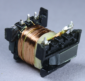
The secondary winding provides the low-voltage high-current output with 8 turns of wire. In order to support 2 amps, this winding has thick wire with four strands in parallel. I haven't seen parallel strands like this before, probably because the KMS charger supplies higher power. Note the 3mm margin tape keeping the winding away from the edge.
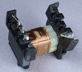
Finally, the second half of the primary winding forms the innermost layer of the transformer; this is also 40 turns of wire. The primary winding is split into two layers that surround the secondary winding for better electrical properties. Note that the primary winding is 80 turns, while the secondary output winding is 8 turns. To oversimplify a bit, this means the output will be 10 times the current of the input at 1/10 the voltage, which is how the high voltage low current input results in the low voltage high current output. The above picture gives a good view of the 3mm margin tape at the right that keeps the wire away from the edge of the core.
Measuring the charger in use
The charger is a switching power supply using a flyback transformer. How this works is the high voltage DC is switched on and off tens of thousands of times a second by the control IC. These pulses of DC are sent into the flyback transformer. A flyback transformer is different from normal transformers in that the output diode blocks power from flowing out of the transformer while power is flowing in. Instead, as the current increases, power is stored in the transformer as a magnetic field. When the input current switches off, the stored power then flows out of the transformer, providing the desired output.
By looking at the output voltage and frequency spectrum, we can determine a fair bit about how the device operates. I measured a constant 60 kHz switching frequency above 1 amp output load, but a dropping frequency for lower loads. The datasheet gives some clues to this behavior. The power supply normally operates using PWM (pulse width modulation). The switching frequency is constant, but the amount of time the power transistor is on varies. The longer it is on, the more power into the transformer and the more output power. This matches the observed behavior from 1 amp to 3.5 amps. The datasheet also describes how the switching frequency drops under low power, which matches what I observed below 1 amp.
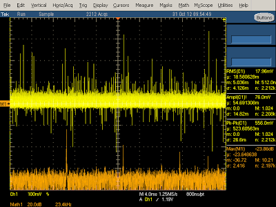
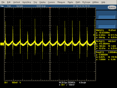
The above oscilloscope trace illustrates the behavior when producing 2 amps. The frequency spectrum shows narrow peaks (orange) at the 60 kHz switching frequency and harmonics. The yellow output voltage shows a bunch of large spikes due to the power switching on and off - this indicates that the charger isn't filtering the output very well, letting these spikes get into the connected device.
The diagram below zooms in to show the output in more detail. Each spike is when the switching transistor turns on at 60 kHz. The output power drops as the current through the flyback transformer increases (since the transformer secondary is blocked by the diode at this time). The output then climbs when the transistor switches off and the power is transferred to the secondary.
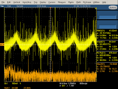
As the charger load increases above 3 amps, the quality of the output significantly decreases, and large 120 Hz ripple appears in the output (yellow). This is probably because the input capacitors can't store enough power to provide a constant output at this high load. Since the charger is only rated to provide 2.1 amps of output, I don't consider this a design flaw, but it's interesting to see this behavior in the output. The key result here is not to overload the charger, because the power quality gets much worse.
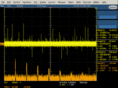
The charger is designed to reduce the switching frequency under low load for efficiency. I found this feature kicks in at loads under 1 amp, with the switching frequency smoothly dropping from 60 kHz to 29 kHz at 250 mA load and even lower under no load. The graph below shows the frequency spectrum at 250 mA load. Note that the spikes are wider than the previous case since the frequency becomes more unstable when it is reduced.
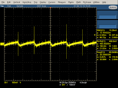
The output waveform below at 250 mA is similar to the previous (2A) case, except at a lower frequency. Note that the output still has large spikes when the transistor switches on. The output voltage drops while the switching transistor is on and then rises while the transistor is off (due to the flyback design), so you can see below that the transistor is off most of the time at low power.
Power consumption
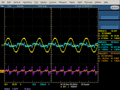
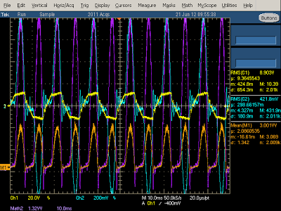
Measuring the power consumption of a charger is tricky because the charger doesn't use power like a normal resistive load, but uses a nonlinear part of the input current. This results in a power factor lower than unity. (You might expect that the poor power factor is because the charger switches on and off thousands of times a second, but actually it's the fault of the diode bridge.) I measured the power consumption of the charger under load by measuring the instantaneous line voltage and current, computing the instantaneous power, and then computing the real power from this.[6] In the following diagrams, the input line voltage is shown in yellow, and the input current is in cyan. The instantaneous power is graphed in orange at the bottom - simply the product of the voltage and current.[7]
The oscilloscope output below shows the power usage of the charger under no load. The line input voltage (yellow) is a nice sine wave, but the current (cyan) is very irregular. There is a bump corresponding to the voltage peaks as the input diodes conduct and re-charge the filter capacitors. The remaining current oscillations are unusual - I haven't seen them in other chargers, and I expect they are due to the large input choke. From the orange line you can see that the power usage has small spikes at 120 Hz. Taking the power factor into account and computing real power shows the charger uses 180 mW when idle which is fairly high, but actually lower than the Apple iPhone charger.
With load applied to the charger, the power usage shoots up as shown below. I compute the power usage as 6.4 watts, while the charger is supplying 4.4 watts to the output, for an efficiency of 69%. The shape of the current curve (cyan) and power curve (orange) shows that the charger is taking line power about half the time (the big curved peaks), and not for the other half (the flat oscillations in between). This illustrates the bad power factor that switching power supplies have. (PC power supplies often use power factor correction (PFC) circuits to improve the power factor.)The yellow input voltage curve is somewhat distorted, probably due to the lame isolation transformer I used.
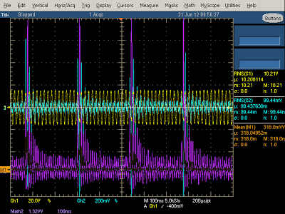
You might wonder what happens if you short-circuit the output of the charger. It is designed to shut down before damage occurs, rather than self-destruct. After the internal voltage drops, the charger will start up again, and repeat this cycle until the problem goes away. This is called "hiccup mode", since the charger generates hiccups of power. The oscilloscope trace below shows the power consumption of the KMS charger when shorted. Note the pulses as it start up and shuts down every 250 milliseconds.
Components
For those who are interested in the components, I have some details. The two 6.8uF 400V electrolytic capacitors in the primary are made by ChengX. The two 470uF capacitors in the secondary are made by JWCO. The X capacitor is a .1uF K 275V X2 made by Dain Electronics, a Chinese manufacturer of plastic metal film capacitors, now merged with WINDAY Electronic Industrial Co Ltd. The Y1 capacitor is a JN222M 2200pF disk ceramic suppression capacitor manufactured by Jya-Nay, a Taiwanese capacitor company. There's also a blue 681J (i.e. .68nF) polyester film capacitor of unknown manufacturer; looking at the circuit board this capacitor (C7) was originally a surface-mounted device, but was replaced with a larger capacitor.The diodes are manufactured by MIC (Master Instrument Corporation, Shanghai). Most chargers use a diode bridge to convert the AC to DC, but this charger uses four independent diodes, which are 1N4007 700V diodes. The secondary rectification uses two Schottky diodes (SR360 3 amp 60V) from MIC. The circuit board uses the unusual mounting of two diodes on top of each other soldered into the same holes. The charger also uses FR107 700V fast recovery diodes.
Like most power supplies, the charger uses a TL431A for the voltage feedback.[1] This TL431A is produced by Wing Shing Computer Components The optocoupler is an ORPC 817B optocoupler from Shenzen Orient Technology Co., Ltd. (I don't want to speculate on the cultural significance of their raising the flag over Iwo Jima company logo.)
Conclusion
The KMS charger occupies an interesting middle ground between dangerous $2 counterfeit chargers and expensive name-brand chargers. Tearing down this 4-port USB charger of unknown origin reveals details of the circuitry. It also illustrates a network of Chinese suppliers and manufacturers, most of which are hardly known in the US. On AmazonNotes and references
[1] To summarize the feedback circuit: R17 and R18 form a resistor divider on the output voltage. If the output voltage is above 5.125 volts, the TL431 control input will be above 2.5 and the TL431 conducts. This energizes the optocoupler, providing current pulling the FB pin lower. Low FB increases the duty cycle, increasing the maximum transformer current, and increasing the output voltage. If the output voltage is considerably too high, or overtemperature is sensed, the switching frequency is decreased, reducing the power transferred to the output. (This is over-simplified; the frequency response of the feedback control loop is controlled via R13, R16, C8, and C9.) An alternative is to sense voltage from the primary side, so the feedback circuit can be eliminated. This reduces the total charger cost by about 20 cents according to a report.
[2] The use of a copper "belly band" in flyback transformers is discussed in Flyback Transformer Design for the UCC28600 (page 2). It provides an electromagnetic radiation shield. The article mentions that the belly band may cause difficulties with creepage requirements and that seems to be the case with the KMS, since there is only 3mm creepage between the primary-grounded belly band and the secondary wiring.
[3] A lot of interesting information about flyback transformer design and construction is in Cookbook for do-it-yourself transformer design
[4] A discussion of how to achieve 5-6mm creepage distance by using 2.5 or 3mm margin tape is in Flyback Transformer Design for the IRIS40xx Series. Note that the margin tape must be on both sides of the winding to achieve this distance, while the KMS transformer only uses the tape on one side.
[5] Safety Considerations in Power Supply Design provides a detailed explanation of safety requirements for power supplies. It explains creepage and clearance
[6] See Understanding power factor and input current harmonics in switched mode power supplies for details on power factor, power supplies have poor power factors, and why poor power factors are a bad thing. Briefly, the power factor is due to the non-linear current through the diodes at peaks, not due to a phase shift. Real power can be measured with an oscilloscope as the average value of the instantaneous power, see Power - Real And Apparent: A Tutorial On Basic Line Power Measurements or Measuring power using the DL750.
[7] For the input power measurements it is very important to use an isolation transformer to avoid destroying your oscilloscope or shocking yourself. For my measurements, a resistor voltage divider reduced the input line voltage - the actual voltage is 11.06 times the displayed probe 1 voltage (C1, yellow). The current was measured through a 5.2 ohm shunt resistor, so the current is 1/5.2 times the displayed probe 2 voltage (C2, cyan). Combining these, the power in watts is 2.13 times the measured C1*C2 value (M1, orange).
cool stuff. What software do you use to generate the schematic figure?
ReplyDeleteBrilliant article, thanks for all the measurements!
ReplyDeleteKen, this is an excellent article, thanks so much for all the work you did, and for sharing it with others. I'm working on DIY solar chargers and inverters, and this is a really helpful article, full of good practical info.
ReplyDeleteKen, this is an excellent article, thanks so much for all the work you did, and for sharing it with others.
ReplyDeleteGreat article - I have a KMS-AC09 which just stopped working - it turns out F1 is blown as a result of a solder bridge next to the control IC.
ReplyDeleteI found the voltage control feedback circuit interesting. The zener diode acts like a voltage controlled SCR. When the voltage reaches the threshold, it clamps down and sends a pulse over the opto isolator. When the PWM chip gets many of these pulses, duty cycle decreases. The inverse is true. When the pulses are lost, PWM shuts down as a safety. Seems like every charger I tear down has this design.
ReplyDeleteI found your site this morning following a post on osnews.
ReplyDeleteThis is really high quality material on so many levels: not only do you reverse engineer cheap chargers in a big way. As a consumer I would be very happy if you only provided the schematics with component values; but that is only the beginning for you, here we get a thorough analyze of component layout, distances and what not from different perspectives (mostly safety but not limited to that). Then, to fully appreciate the product you provide us not only with the manufacturer for differnt parts of the kit and for the full shebang, we get a set of likely suspects whenever you are in doubt about the origin. On top of that we get a proper performance rundown with an interesting set of (well explained) tests.
I would have been more than happy finding just this, but you do not stop there, you make both power supplies and manufacturing sound interesting and exciting, that is a great achievement!
And you back all this up with nice prose and a dose of wit.
Keep up with the good work!
Ken, Would you please also analyze the following?
ReplyDeletehttp://www.amazon.com/Skiva-PowerFlow-Smartphones-Universal-Compatibility/dp/B008R97TOQ/ref=sr_1_1?ie=UTF8&qid=1361924629&sr=8-1&keywords=quadfire
thanks,
Jay (I PMed you as well.)
Sorry if this is an obvious question.
ReplyDeleteDoes this unit provide 2A at each usb port simultaneously (I could charge 4 phones at 2A each)? or 2A in total across the 4 ports?
Thanks for taking the time to write the article, was very interesting
Thank you, excellent work
ReplyDeleteI almost bought this charger via aliexporess. So glad for such a article to explain the good and bad.
ReplyDeletedo you have picture how to open the casing properly ?
ReplyDeleteKoh Wee Chai: the best way I've found to open chargers is to use a hammer and wood chisel and tap them around the seam. This will usually break the weld between the two parts of the case without breaking the case itself.
ReplyDeleteAmazing post. While most of it wasn't useful to me (that's just the parts I understood) this level of detail and minute investigation should be respected and lauded no matter what the subject.
ReplyDeleteGood show, sir. Good show.
Ken, suppose I wanted to intergrate an RF 5-24V receiver into the assembly. Where would be an ideal place to cut in at? Each USB output I have is ran to a single high power LED.
ReplyDeletedear sir can u explain me how flyback circuit going on off.http://ahmedx.hubpages.com/hub/How-To-Use-A-Flyback-Transformer-As-A-Tesla-Coil-How-To-Convert-12V-DC-To-Thousands-Of-Volts#slide6203171
ReplyDeleteI have two of these adapters. (One charges my devices at night (as well as powering a nearly dead-battery first generation iPod touch running a basic bedside alarm clock app). I use my second to power a Raspberry Pi computer sometimes for weeks/months at a time, also in my room. I don't overload the supply on either, maximum a little over 1000mA drawn - a far cry from 4*500mA USB devices)
ReplyDeleteAnyway, my question is will this kill me at night? I'm specifically worried about catching fire. It's quite near my head at night and another would block my escape route in the event of a fire. (I know the dangers high voltage reaching the output, but not of failure).
I can't afford $30 for Apple charger, but can afford $5-$15 for something safer, I hope to upgrade from the $4 KMS AC09.
Thanks! I really hope you or somebody gives me a reasonable answer!
Great teardown! I have two of these and so far have not had any problems with them, charging up to three 2A devices at once. But I like to know what's inside stuff I own. The question that lead me to this post was if there was any difference between the two pairs of ports. Now I know:)
ReplyDeleteI bought it from
ReplyDeletehttp://www.youbeli.com/port-usb-ac-wall-charger-adapter-plug-for-mobile-devices-28tc09ig29-p-388209.html
is this the same of what you have teardown?
I have one of these recently and when charging on iPad air it works fine, today when I try to charge it with one iPad Air, one iPad 1 and connect wireless charging base to charge my iphone, it crashes and doesn't work anymore. The blue led light doesn't light up anymore, I guess its 'fried'.... anyway I can open up and do something to it? Kind of waste as it comes with the pounch and all the universal adaptor
ReplyDeleteHello, i bought this charger last week so my family could all charge their phone at night. Now everyone's phone battery is broken! My phone (htc one x) can only last for 2 hours now. I am very angry, especially since there is no clear manufacturer to send an email to. Can you explain how this charger could mess up phone batteries?
ReplyDeleteI thank you, Ken, for your stirling work. I want to see much more of this sort of information on-line than the 99.99999% trash that I usually come across. You are a scholar and a gentleman. :-)
ReplyDeleteThe device can support max of 12 W means at 5 V it can deliver 2.4 A max
ReplyDeleteThis dies not have charge standard ic at output which is all needed for apple and BB and others but they had resisters alone wi avoid ch to reduce cost
!2 w dissipation need heat sink and need esd protection circuits for safety
Is it possible to remove the LED's without too much damage to the unit?
ReplyDeleteHow is best to get it to bits?
Thanks
Thanks for the article on this USB charger. With you information I was able to make an informed buying decision against this product and will purchase a name brand product. Thanks for your attention to detail when breaking this item down. Great work.
ReplyDeleteI removed the LED's successfully.
ReplyDelete1. Pry open with a large screwdriver from the 2 slits near the power plug.
The unit seems to be glued together.
2. remove the circuit board and find the LED's and break them. Make sure the wires left are not touching each other or the USB frame.
3. Put the circuit board back in. Put the button and sliding plate back in. Use tweezers to place the little spring in place that holds the button and sliding plate.
4. Glue the unit back together.
Job done.
Blue LEDs are good at resetting mammals' circadian clocks. IOW, they can be bad for sleep.
ReplyDeleteGreat article. Mine broke and today I opened it up. Interesting mine has even less parts(filter capacitors in the primary side) which part would break? My guess it's the control ic as the rest seem to measure just fine)
ReplyDeleteEdo, if your charger quit, my guess would be the switching transistor failed since it's probably the most-stressed component. But it could be the control ic.
ReplyDeleteThank you for your prompt reply. If I read your article correct the switching transistor in this case is inside the thx203h control ic right?would it make sense to put a small cooling block on that ic after I replace it since the charger failed under load and it got really hot . also my charger is cheaper missing the choke and x capacitor. It's just empty on the pcb. Would this have any effect on charging?
ReplyDeleteEdo, you're right - I forgot that this charger doesn't have a separate switching transistor. The missing components might make the charger radiate more noise and produce lower-quality power. A heat sink on the IC might help, but it would be easier to get a new charger.
ReplyDeleteI bought two of these in early 2015 under the Korjo brand name in Australia. One seems to work fine (no obvious problems charging an iPhone 4S, an iPad Air2, and a compact camera). The other one caused bizzare behaviour (phantom touches and drags all over the place) on an iPad Air touchscreen while the iPad was charging from the Korjo and I suspect that the Korjo was responsible for damage to the battery circuitry in my iPhone 5S. After using the charger, the iPhone was losing 10% of the battery charge per hour even in standby and even after a full restore to factory state. Apple replaced the iPhone even though it was out of warranty. I called Korjo, in Australia, and asked them about it and they promptly replaced the charger at no cost. They said they had a bad batch at one point, but I won't be taking a chance with it after reading your excellent article, Ken.
ReplyDeleteGreat write-up - thanks for this!
ReplyDeleteGot it fixed. Replaced the thx203h-7v and one of the sr360 (one was faulty) added a small heatsink to the thx203h.. All seems well now.. Great blog.. Thx again!
ReplyDeleteHi Ken,
ReplyDeleteNice write-up.
Regarding the isolation, it appears that the transformer uses 3mm tape on the secondary side next to the primary windings, and vice versa on the secondary winding. If true, and the bobbin gives adequate clearance, sufficient isolation may be present. 3mm will be from the margin tape, and from there 2-3mm will be required (the requirements change and it's possible only 5mm was required). On top of that, different inspectors have their own pet peeves or may miss a design error. But based on the quite-reasonable design I see elsewhere, I suspect approval may be possible. (Why it isn't approved is a mystery.)
Regarding power measurements, have you aligned your probes? Having the current and voltage improperly time-aligned will easily cause mW of error, which is significant in your case.
Also, you mention spikes but don't talk about your probes or the measurement method. It's so, so easy to see false spikes to due suboptimal measurement methods. From my experience, it's far to easy to blame a circuit for spikes when the real culprit is me. Getting the parasitics of the probes low enough to accurately see spikes is challenging.
Hi, can you tell me why when i want to plug more than one appliance, there is a continuous bip sound ? Thank you very much.
ReplyDeleteHi Ken
ReplyDeleteI know your article and this thread is rather old, but I have one of these chargers (at least it looks exactly like this from the outside...). It has been working nicely for quite a while, but recently the blue light started flashing and it's not charging any more.
Did you come across anything that could cause this, or have a general idea what it could be? And more importantly, do you think it's something I could fix easily? I know it's probably not worth the hassle, but I like the "travelability" of it :-)
If it simply didn't work anymore, I would accept that it's dead, but I think the flashing might be a sign that it's just something simple that could be fixed.
Thank you lots
Cheers
Joa
Joa, if the output is shorted, the charger will start up and shut down about 4 times a second - does that match the flashing of the blue light? It must be working at least somewhat in order to light the LED, and then decides to shut down repeatedly. But it could be any component that failed in the charger. Personally, I'd just get a new one.
ReplyDeleteHi, Ken!
ReplyDeleteI have MAXXTER charger, model ACT-U4AC-01-2 (http://www.maxxter.biz/item.aspx?id=8975).
This is full analog HICONN 4-Ports USB Wall Charger (http://www.hiconn.net/product/124-en.html).
In this charger used chip HiCONN 124 (analog SW2604 - http://www.semipower.com.cn), analog THX203H too.