The Yamaha DX7 digital synthesizer (1983) was the classic synthesizer for 1980s pop music. It used two custom digital chips to generate sounds with FM synthesis. In this blog post, I examine the log-sine ROM that digitally produces sine waves inside one of these chips. (This blog post jumps into the details; unless you care about the sine values specifically, my previous DX7 reverse-engineering article is probably more interesting.)
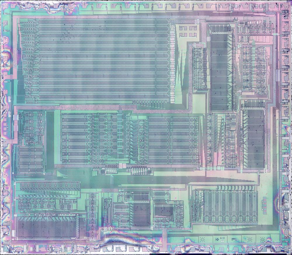
I created the high-resolution die photo below by compositing over a hundred microscope photos. I removed the metal layer from the chip with acid to reveal the silicon and polysilicon wiring underneath. You can see the structure of the functional blocks and the connections between them. The colors are due to variations in thickness of the oxide layer, causing thin-film interference. With the metal layer removed, I could read out the bits from the ROM, reverse-engineer the circuitry, and determine the exact values used for sine-wave generation.
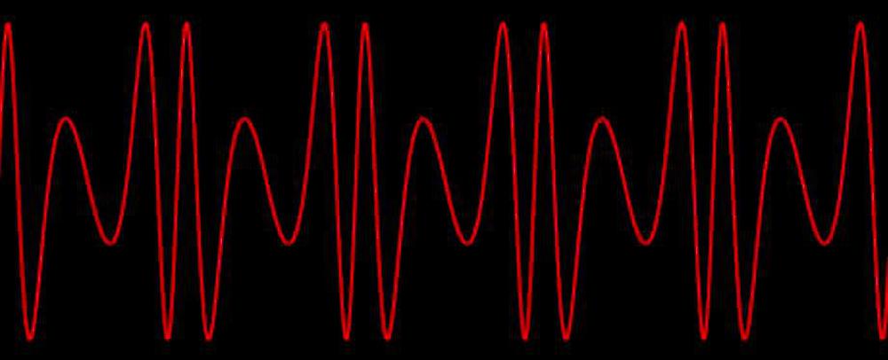
Instead of the analog oscillators and filters of an analog synthesizer, the DX7 generates sounds digitally, using a technique called FM synthesis. The idea is that you start with a sine wave (the carrier signal) and perturb it with another signal (the modulating signal). The modulating signal changes the phase (and thus the frequency) of the carrier, creating complex harmonic structures like the waveform below. These signals are represented as digital values throughout the system; a digital-to-analog converter (DAC) turns the digital representation into an analog voltage for the synthesizer's output.
The digital implementation of frequency modulation uses a lookup table that holds a digitized sine wave. By stepping an index through the table at a specific rate, you can produce a sine wave of a fixed frequency. By perturbing this index with another signal, you can produce a modulated sine wave like the one below. The DX7 implements this with a sine-wave table in ROM, an increment value that controls the frequency, and an adder that adds the increment to the table index (i.e. the phase angle) each time step. This ROM is the subject of this blog post.
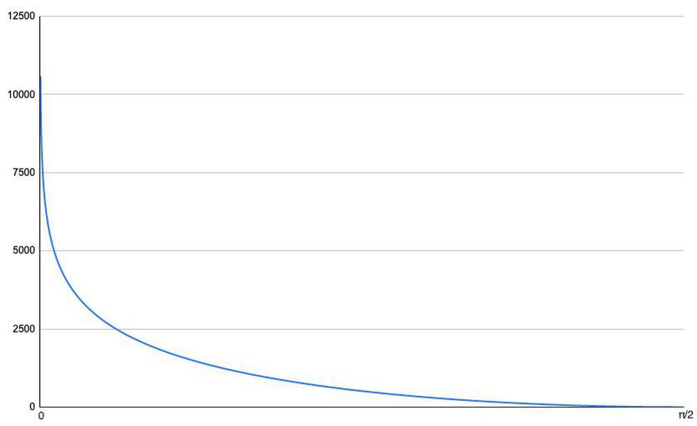
The amplitude of the sine wave is controlled by an envelope, varying over time; multiplying the sine wave by the envelope level yields the output. However, fast multiplication required too much hardware in the 1980s, so the DX7 uses a mathematical shortcut: adding logarithms is equivalent to multiplying the values. The obvious problem is that computing logarithms is harder than multiplying, but the trick is to store the (negated) logarithm of the sine wave in the lookup table (below) instead of the sine wave. This provides the logarithm for free. (The other issue is that you need to perform an exponential to get the final result. I described the exponential ROM and circuit in my previous DX7 article).
The block diagram below shows the structure of the log-sine circuit, computing a 14-bit value from a 12-bit input. The circuitry is somewhat complex to fit a fast, high-accuracy calculation into a small space on the die. The implementation takes advantage of the symmetry of the sine wave so only a quarter-wave needs to be stored. The top bit is used as the sign bit, which inverts the output elsewhere to obtain the negative half of the sine wave. (This also avoids the problem of taking the log of a negative value.) The second bit implements the mirror symmetry of each sine-wave peak by inverting the bits for the second half of the peak.
The ROM and associated logic take a 10-bit input address representing a quarter of the sine wave (angles 0 through π/2). A technique called delta encoding is used to reduce the size of the ROM. The idea of delta encoding is that if values change slowly, the difference between two values is considerably smaller than the value itself.1 Specifically, only every fourth value is explicitly stored in the ROM; this value is called an "absolute" value.3 The next three values are stored as deltas: the difference between the value and the previous absolute value.2 An adder circuit adds the absolute value to the difference value, yielding the desired log-sin value.
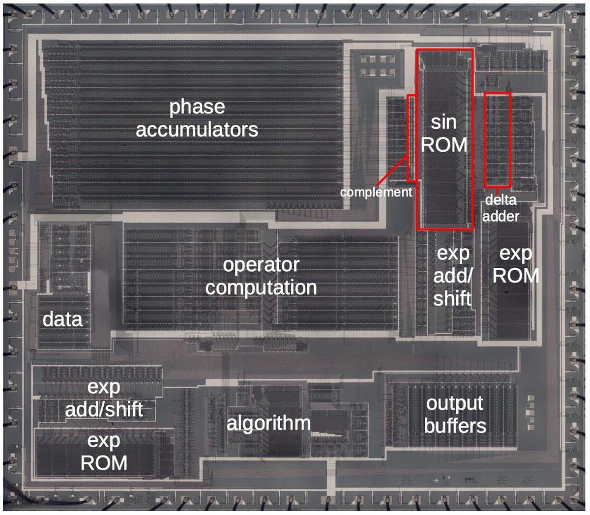
The diagram below labels the main functional blocks of the chip. In this article, I focus on the sine circuit, highlighted in red, but I'll summarize the other blocks. The 96 phase accumulators, implemented with shift registers, are the largest block of the chip. They hold the current table index for each of the DX7's 96 oscillators. The exponential function is implemented by two identical ROMs and associated addition/shifter circuitry. Other major blocks apply the envelope, hold configuration data, compute the operators that combine oscillators, define different operator algorithms, and buffer the output values.
The ROM
The photo below shows the log-sin ROM. The ROM itself consists of a grid of transistors. At the top, decoder circuits select signal lines based on the address bits. At the right, the diagonal circuits are multiplexers, selecting particular rows of the ROM. To the right of the multiplexers, logic circuits select the delta values. I won't explain these circuits in detail since I discussed the similar circuits for the exponential ROMs in my previous article.
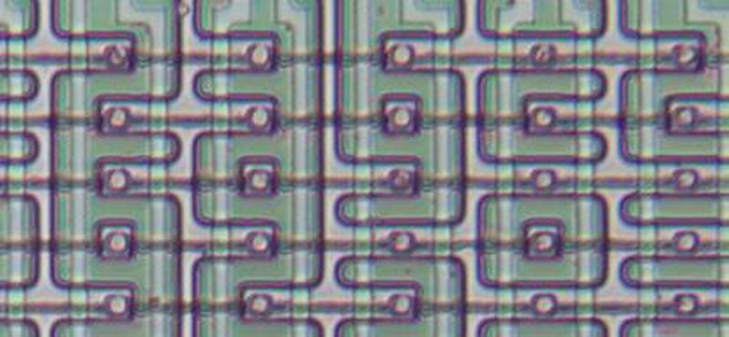
By examining the ROM closely, you can see the individual transistors that store bits. A transistor represents a 1, and the lack of a transistor represents a 0. Thus, the data in the ROM is created by the pattern of how the silicon is doped. I was able to read out the ROM data visually by looking at this pattern.
The delta representation and the adder
The ROM itself produces 43 output bits, 13 bits for the "absolute" value and 30 bits for the three delta values. Some logic circuitry expands the ROM's 30 bits into three deltas of 12 bits (and a zero delta for the absolute value), taking advantage of some structure in the deltas. This circuitry is just to the right of the ROM and is implemented with AND-OR-INVERT gates. These gates implement 4-to-1 multiplexers, selecting the appropriate delta value based on the 2 lowest input bits.
Next, the adder circuit to the right of the ROM adds the 13-bit absolute value and the 12-bit delta value to generate the final 14-bit value. One interesting feature of the adder is it is pipelined to minimize the delay from carry propagation. I discussed the adder implementation in my previous article so I won't go into details here. The adder is immediately followed by a second adder that adds the envelope value to scale the signal level, taking advantage of the logarithmic representation.
Overall, the log-sine circuit generates 1024 14-bit values. Stored directly, this would take over 14 kilobits, but the ROM is only 5344 bits. The delta representation and ROM compression reduce the ROM size by almost 63%, important for a chip built in the 1980s when transistors were precious. By itself, the delta representation doesn't save much space: a 12-bit delta instead of a 14-bit value. But the ROM's implementation makes the deltas efficient: if a 32-bit row in the ROM is all zeroes, the row can be omitted entirely and the output defaults to 0. For the flat parts of the function, the high-order bits of the deltas are mostly zero, so much of the ROM can be omitted.
Conclusion
The DX7 generates its waveforms from a digital sine wave, so producing a high-accuracy value rapidly is key to the synthesizer's performance. By examining the ROM and associated circuitry, I could obtain the exact values that the DX7 uses for the log-sine function. The ROM provides one quarter of the sine wave and the other quarters are formed by symmetry. For a 10-bit input value n, the corresponding angle is ω = (n + .5)/1024×π/24 and output value y is -log2(sin(ω)), represented as the integer round(y×1024).5
I plan to continue investigating the DX7's circuitry, so follow me on Twitter @kenshirriff for updates. I also have an RSS feed.
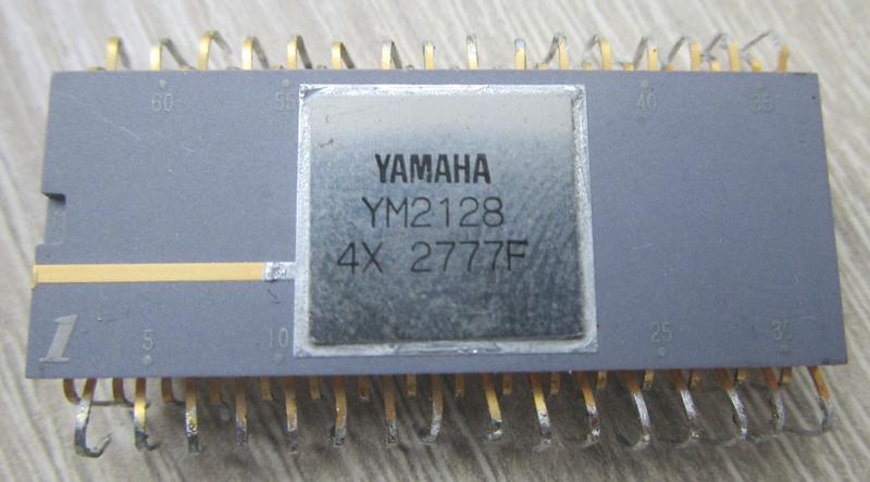
Thanks to Jacques Mattheij and Anthony Richardson for providing the chip and discussion.6
Notes and references
-
A different chip, the Yamaha YMF262 (1988) was used in computer sound cards such as the Sound Blaster 16. (This chip is also known as OPL3 for FM Operator Type-L.) It uses FM synthesis, but is stripped down compared to the DX-7. The chip was reverse-engineered by Matthew Gambrell and Olli Niemitalo who decapsulated the chip and read out the ROM contents.
The OPL3 log-sine ROM is similar to the DX7's in some ways, but is lower resolution. The OPL3 chip is 256 samples long, rather than 1024, and holds 8-bit values, rather than 13-bit values. Both chips use delta encoding, but the OPL3 has one delta-encoded value for each absolute value, while the DX7 has three delta-encoded values. ↩
-
To be precise, the three delta values are stored before the absolute value in the ROM. That is, entries 3, 7, 11, ... are absolute, instead of 0, 4, 8, ..., the expected locations. I think this is because the log-sin function is decreasing, so if you want to add the deltas (instead of subtracting), the absolute value needs to be the last of the group, not the first. ↩
-
The absolute value in delta encoding is the full, explicit value. It's unrelated to the absolute value function |x|. ↩
-
Note that the input to the ROM is incremented by half a bit. This avoids duplication of the 0 value of the waveform when the quarter-wave is mirrored. It also avoids computation of the undefined value log(0). ↩
-
The value is rounded to an integer by computing int(y×1024 + .5002). The constant .5002 rounds the value up, with just a tiny bit more that affects a single entry. I'm not sure why the rounding is not exact; perhaps Yamaha used a lower-precision sine or logarithm, which was just enough to change one bit. (Note that the value .0002 is somewhat arbitrary; a slightly larger or smaller number will yield the same result.) ↩
-
For more information on the DX7 internals, see DX7 Technical Analysis, DX7 Hardware, OPLx decapsulated, and my previous DX7 articles Reverse-engineering the Yamaha DX7 synthesizer's sound chip from die photos and The Yamaha DX7's exponential circuit. ↩


Huh, so deltas need to be 12-bit for 14-bit base values this time? That's... quite a scale change compared to exp function circuit, alright...
ReplyDeleteIn an early paragraph, you seem to mention those very same exp ROM 4 bit wide deltas though. Typo, I guess?
In regards to the log-sin function. You seem to be using a small logarithm base, which extends to footnote mentioning the function being decreasing; when I asked my computer for a log-sin plot to see why those deltas are what they are, it was very much increasing over first quarter of the circle... though in negative domain. I guess your convention is not wrong, but it's something to watch out for when most people seem to default to 2, e, or 10 for logarithm bases, which are all above one.
Thanks for the read. I hope I do not come off as too whiney.
Hi Stan. Thanks for your comments. Yes, the deltas for log-sin are much larger than for 2^x (which is close to linear over 0-1 interval), because log-sin is asymptotically steep near 0. You are correct that "4-bit deltas" is an error, a bad cut-and-paste from my exponential article.
ReplyDeleteThe logarithm base is base 2, which works out well in binary. Since sine is <=1, the logs are all negative. I flipped the sign to positive, which is how (I think) they are stored in the ROM, but I didn't make the sign change clear.
Are you sure that it's really just 30 bits of deltas? I count 32 (12+11+9).
ReplyDeleteKeyJ: It depends what you're counting. For the 12-bit delta and 11-bit delta, the second bit is always 0, so it's not stored in the ROM.
ReplyDeleteNevermind. My code did in fact find and use those two all-0 colums (and I end up with the correct ROM size of 5344 bits as a result), it's just that it displayed the position of the highest bit instead of the number of actually used bits.
ReplyDeleteKeyJ: It seems like you're working on something interesting. If you want to get in touch by email, my contact info is in the sidebar.
ReplyDeleteHello. I didn't know about your work, else I might have learned a lot here, but maybe it's more recent than when I interpreted what I saw on Olli Niemitalo's page. Anyway, I ended up making a software emulation of the DX5, it's on my web site. It's not an exact replica, I used half cycles for easier coding and higher efficiency, and a cosine wave instead of sine, for manipulations various (that my BlueStar synth doesn't do, but my later work will, when released). Instead of precise emulation of existing details, I came up with my own methods, not least because I saw the DX7 as brilliant, but flawed, in aspects of the EG's the LFO, and the fine tuning, and fine scaling. Even so, I am always in some kind of awe at the efforts to decode directly based on observations of the IC's used! While I got by mostly with service manuals and expired patents and a LOT of experimentation over ten years, it was these direct observations that helped me to limit my efforts and avoid notions that would have been impractical.
ReplyDeleteIf you or anyone wants to try BlueStar, it's at the site linked to in this post. You might need the odd red pill, but the rabbithole is not too deep.
Your footnote 5 is interesting.. I do things like that subscale offset when avoiding threshold detection problems with floating point imprecision, but I think Yamaha used integer arithmetic! I know I did, in BlueStar. I could have used FP but the complications put me off, I preferrered to stay with the precision that integers allowed, because 32 bits is downright luxury! :) Though my cosine wave is a log for 12 bits (and sign on restoration, same as Yamaha did it), but I use more res elsewhere to get a cleaner result in scalings, tunings, EG's.. I used a 12-bit interpolator in the mod input system too, so those of you who hate 'zipper noise' in the EG bias controls might want to try BlueStar.
ReplyDelete