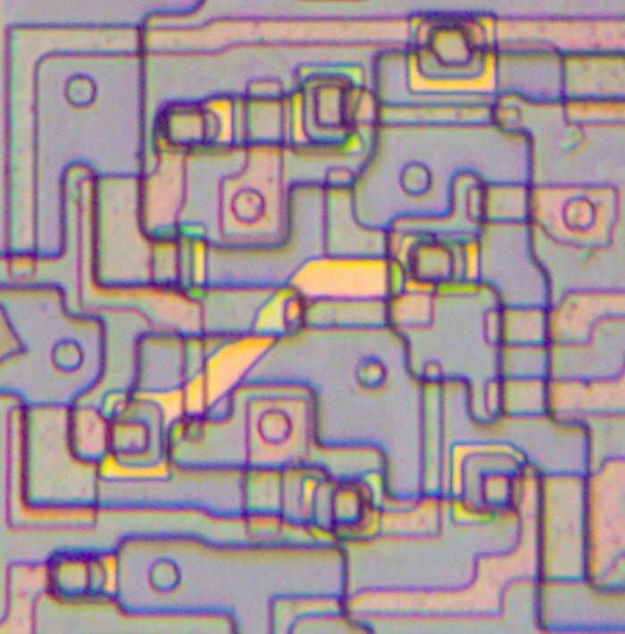
I've studied a lot of chips from the 1970s and 1980s, so I usually know what to expect. But an Ethernet chip from 1982 had something new: a strange layer of yellow wiring on the die. After some study, I learned that the yellow wiring is a second layer of resistive polysilicon, used in the chip's static storage cells and latches.
The die photo above shows a closeup of a latch circuit, with the diagonal yellow stripe in the middle. For this photo, I removed the chip's metal layer so you can see the underlying circuitry. The bottom layer, silicon, appears gray-purple under the microscope, with the active silicon regions slightly darker and bordered in black. On top of the silicon, the pink regions are polysilicon, a special type of silicon. Polysilicon has a critical role in the chip: when it crosses active silicon, polysilicon forms the gate of a transistor. The circles are contacts between the metal layer and the underlying silicon or polysilicon. So far, the components of the chip match most NMOS chips of that time. But what about the bright yellow line crossing the circuit diagonally? That was new to me. This second layer of polysilicon provides resistance. It crosses over the other layers, connected to the silicon at the ends with a complex ring structure.
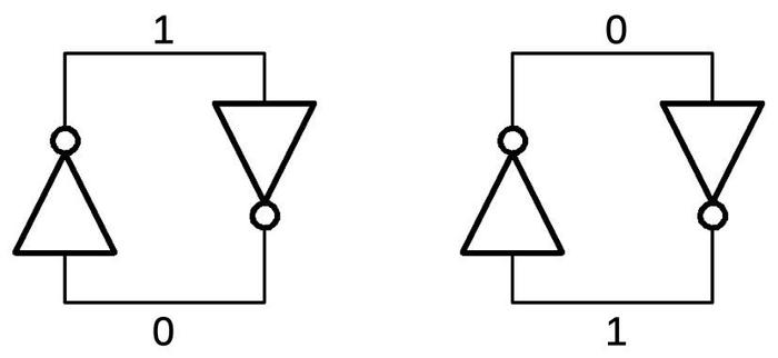
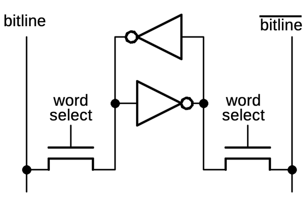
Why would you want high-resistance wiring in your digital chip? To understand this, let's first look at how a bit can be stored. An efficient way to store a bit is to connect two inverters in a loop, as shown below. Each inverter sends the opposite value to the other inverter, so the circuit will be stable in two states, holding one bit: a 1 or a 0.
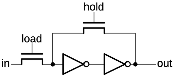
But how do you store a new value into the inverter loop? There are a few techniques. One is to use pass transistors to break the loop, allowing a new value to be stored. In the schematic below, if the hold signal is activated, the transistor turns on, completing the loop. But if hold is dropped and load is activated, a new value can be loaded from the input into the inverter loop.
An alternative is to use a weak inverter that produces a low-current output. In this case, the input signal can simply overpower the value produced by the inverter, forcing the loop into a new state. The advantage of this circuit is that it eliminates the "hold" transistor. However, a weak inverter turns out to be larger than a regular inverter, negating much of the space saving.1 (The Intel 386 processor uses this type of latch.)
A third alternative, used in the Ethernet chip, is to use a resistor for the feedback, limiting the current.2 As in the previous circuit, the input can overpower the low feedback current. However, this circuit is more compact since it doesn't require a larger inverter. The resistor doesn't require additional space since it can overlap the rest of the circuitry, as shown in the photo at the top of the article. The disadvantage is that manufacturing the die requires additional processing steps to create the resistive polysilicon layer.
In the Ethernet chip, this type of latch is used in many circuits. For example, shift registers are built by connecting latches in sequence, controlled by the clock signals. Latches are also used to create binary counters, with the latch value toggled when the lower bits produce a carry.
The SRAM cell
It would be overkill to create a separate polysilicon layer just for a few latches. It turns out that the chip was constructed with AMD's "64K dynamic RAM process". Dynamic RAM uses tiny capacitors to store data. In the late 1970s, dynamic RAM chips started using a "double-poly" process with one layer of polysilicon to form the capacitors and a second layer of polysilicon for transistor gates and wiring (details).
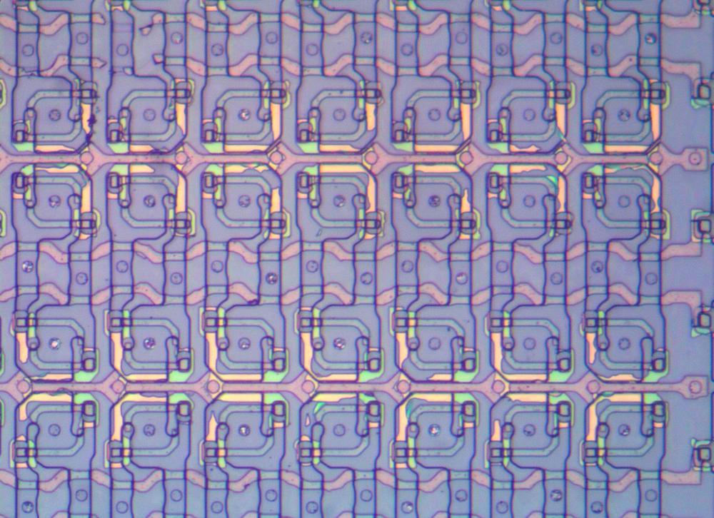
The double-poly process was also useful for shrinking the size of static RAM.3 The Ethernet chip contains several blocks of storage buffers for various purposes. These blocks are implemented as static RAM, including a 22×16 block, a 48×9 block, and a 16×7 block. The photo below shows a closeup of some storage cells, showing how they are arranged in a regular grid. The yellow lines of resistive polysilicon are visible in each cell.
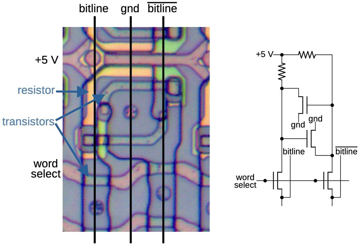
A static RAM storage cell is roughly similar to the latch cell, with two inverters in a loop to store each bit. However, the storage is arranged in a grid: each row corresponds to a particular word, and each column corresponds to the bits in a word. To select a word, a word select line is activated, turning on the pass transistors in that row. Reading and writing the cell is done through a pair of bitlines; each bit has a bitline and a complemented bitline. To read a word, the bits in the word are accessed through the bitlines. To write a word, the new value and its complement are applied to the bitlines, forcing the inverters into the desired state. (The bitlines must be driven with a high-current signal that can overcome the signal from the inverters.)
The diagram below shows the physical layout of one memory cell, consisting of two resistors and four transistors. The black lines indicate the vertical metal wiring that was removed. The schematic on the right corresponds to the physical arrangement of the circuit. Each inverter is constructed from a transistor and a pull-up resistor, and the inverters are connected into a loop. (The role of these resistors is completely different from the feedback resistors in the latch.) The two transistors at the bottom are the pass transistors that provide access to the cell for reads or writes.
The layout of this storage cell is highly optimized to minimize its area. Note that the yellow resistors take almost no additional area, as they overlap other parts of the cell. If constructed without resistors, each inverter would require an additional transistor, making the cell larger.
To summarize, although the double-poly process was introduced for DRAM capacitors, it can also be used for SRAM cell pull-up resistors. Reducing the size of the SRAM cells was probably the motivation to use this process for the Ethernet chip, with the latch feedback resistors a secondary benefit.
The Am7990 LANCE Ethernet chip
I'll wrap up with some background on the AMD Ethernet chip. Ethernet was invented in 1973 at Xerox PARC and became a standard in 1980. Ethernet was originally implemented with a board full of chips, mostly TTL. By the early 1980s, companies such as Intel, Seeq, and AMD introduced chips to put most of the circuitry onto VLSI chips. These chips reduced the complexity of Ethernet interface hardware, causing the price to drop from $2000 to $1000.
The chip that I'm examining is AMD's Am7990 LANCE (Local Area Network Controller for Ethernet). This chip implemented much of the functionality for Ethernet and "Cheapernet" (now known as 10BASE2 Ethernet). The chip handles serial/parallel conversion, computing the 32-bit CRC checksum, handling collisions and backoff, and recognizing desired addresses. The chip also provides DMA access for interfacing with a microcomputer.
The chip doesn't handle everything, though. It was designed to work with an Am7992 Serial Interface Adapter chip that encodes and decodes the bitstream using Manchester encoding. The third chip was the Am7996 transceiver that handled the low-level signaling and interfacing with the coaxial network cable, as well as detecting collisions if two nodes transmitted at the same time.
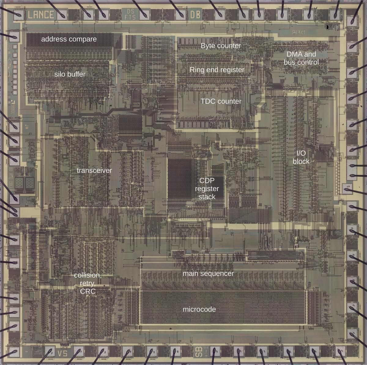
The LANCE chip is fairly complicated. The die photo below shows the main functional blocks of the chip. The chip is controlled by the large block of microcode ROM in the lower right. The large dark rectangles are storage, implemented with the static RAM cells described above. The chip has 48 pins, connected by tiny bond wires to the square pads around the edges of the die.
Thanks to Robert Garner for providing the AMD LANCE chip and information, thanks to a bunch of people on Twitter for discussion, and thanks to Bob Patel for providing the functional block labeling and other information. For more, follow me on Twitter @kenshirriff or RSS for updates. I'm also on Mastodon occasionally as @[email protected].
Notes and references
-
It may seem contradictory for a weak inverter to be larger than a regular inverter, since you'd expect that the bigger the transistor, the stronger the signal. It turns out, however, that creating a weak signal requires a larger transistor, due to how MOS transistors are constructed. The current from a transistor is proportional to the gate's width divided by the length. Thus, to create a more powerful transistor, you increase the width. But to create a weak transistor, you can't decrease the width because the minimum width is limited by the manufacturing process. Thus, you need to increase the gate's length. The result is that both stronger and weaker transistors are larger than "normal" transistors. ↩
-
You might worry that the feedback resistor will wastefully dissipate power. However, the feedback current is essentially zero because NMOS transistor gates are essentially insulators. Thus, the resistor only needs to pass enough current to charge or discharge the gate. ↩
-
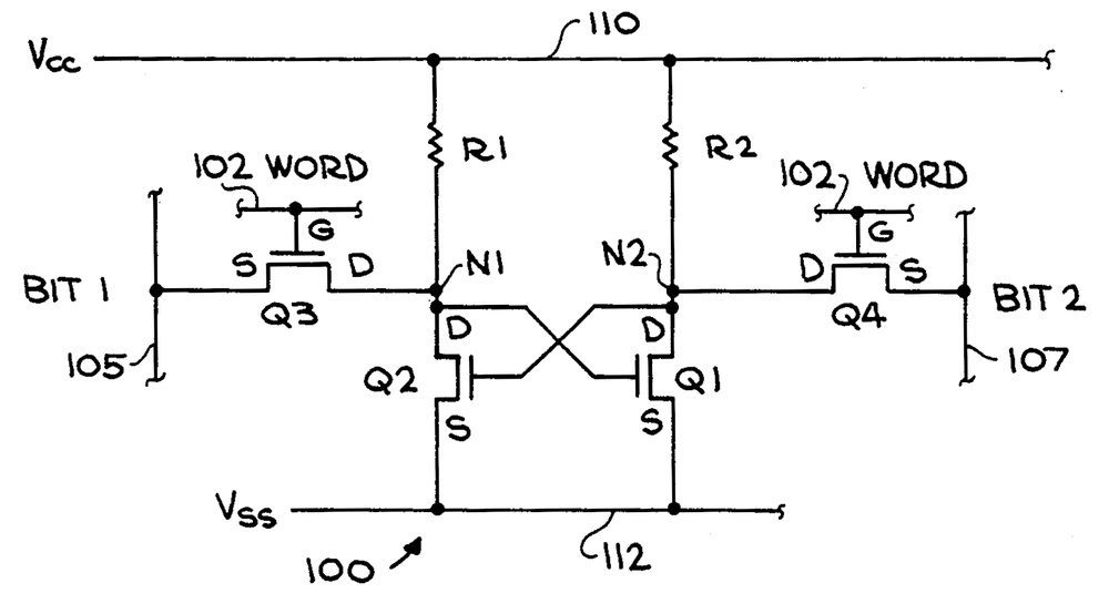
An AMD patent describes the double-poly process as well as the static RAM cell; I'm not sure this is the process used in the Ethernet chip, but I expect the process is similar. The diagram below shows the RAM cell with its two resistors. The patent describes how the resistors and second layer of wiring are formed by a silicide/polysilicon ("inverted polycide") sandwich. (The silicide is a low-resistance compound of tantalum and silicon or molybdenum and silicon.) Specifically, the second layer consists of a buffer layer of polysilicon, a thicker silicide layer, and another layer of polysilicon forming the low-resistance "sandwich". Where resistance is desired, the bottom two layers of "sandwich" are removed during fabrication to leave just a layer of polysilicon. This polysilicon is then doped through implantation to give it the desired resistance.
The static RAM cell from patent 4569122, "Method of forming a low resistance quasi-buried contact".The patent also describes using the second layer of polysilicon to provide a connection between silicon and the main polysilicon layer. Chips normally use a "buried contact" to connect silicon and polysilicon, but the patent describes how putting the second layer of polysilicon on top reduces the alignment requirements for a low-resistance contact. I think this explains the yellow ring of polysilicon around all the silicon/polysilicon contacts in the chip. (These rings are visible in the die photo at the top of the article.) Patent 4581815 refines this process further.


No comments:
Post a Comment