Reverse engineering the 386 processor's prefetch queue circuitry

In 1985, Intel introduced the groundbreaking 386 processor, the first 32-bit processor in the x86 architecture. To improve performance, the 386 has a 16-byte instruction prefetch queue. The purpose of the prefetch queue is to fetch instructions from memory before they are needed, so the processor usually doesn't need to wait on memory while executing instructions. Instruction prefetching takes advantage of times when the processor is "thinking" and the memory bus would otherwise be unused.

In this article, I look at the 386's prefetch queue circuitry in detail. One interesting circuit is the incrementer, which adds 1 to a pointer to step through memory. This sounds easy enough, but the incrementer uses complicated circuitry for high performance. The prefetch queue uses a large network to shift bytes around so they are properly aligned. It also has a compact circuit to extend signed 8-bit and 16-bit numbers to 32 bits. There aren't any major discoveries in this post, but if you're interested in low-level circuits and dynamic logic, keep reading.

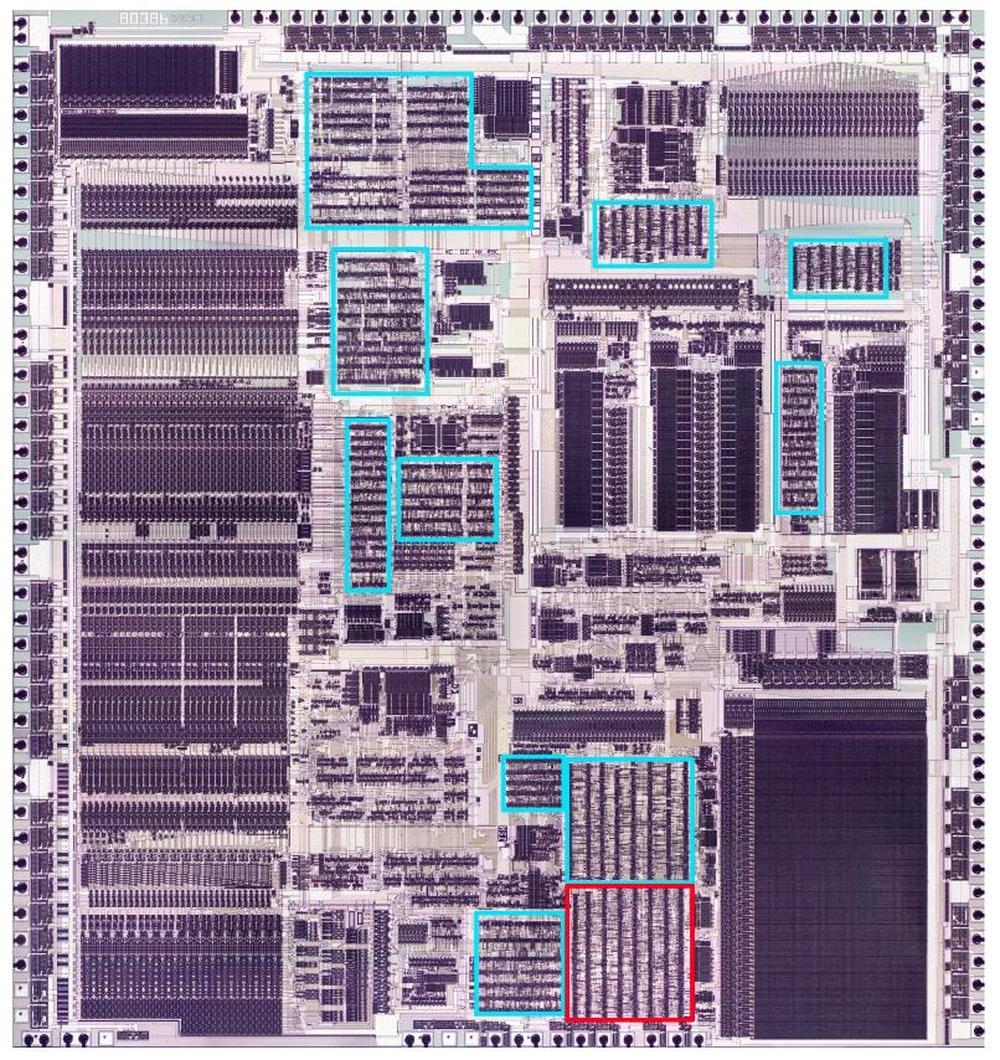
The photo below shows the 386's shiny fingernail-sized silicon die under a microscope. Although it may look like an aerial view of a strangely-zoned city, the die photo reveals the functional blocks of the chip. The Prefetch Unit in the upper left is the relevant block. In this post, I'll discuss the prefetch queue circuitry (highlighted in red), skipping over the prefetch control circuitry to the right. The Prefetch Unit receives data from the Bus Interface Unit (upper right) that communicates with memory. The Instruction Decode Unit receives prefetched instructions from the Prefetch Unit, byte by byte, and decodes the opcodes for execution.

This die photo of the 386 shows the location of the registers. Click this image (or any other) for a larger version.

This die photo of the 386 shows the location of the registers. Click this image (or any other) for a larger version.

The left quarter of the chip consists of stripes of circuitry that appears much more orderly than the rest of the chip. This grid-like appearance arises because each functional block is constructed (for the most part) by repeating the same circuit 32 times, once for each bit, side by side. Vertical data lines run up and down, in groups of 32 bits, connecting the functional blocks. To make this work, each circuit must fit into the same width on the die; this layout constraint forces the circuit designers to develop a circuit that uses this width efficiently without exceeding the allowed width. The circuitry for the prefetch queue uses the same approach: each circuit is 66 µm wide1 and repeated 32 times. As will be seen, fitting the prefetch circuitry into this fixed width requires some layout tricks.

What the prefetcher does

The purpose of the prefetch unit is to speed up performance by reading instructions from memory before they are needed, so the processor won't need to wait to get instructions from memory. Prefetching takes advantage of times when the memory bus is otherwise idle, minimizing conflict with other instructions that are reading or writing data. In the 386, prefetched instructions are stored in a 16-byte queue, consisting of four 32-bit blocks.2

The diagram below zooms in on the prefetcher and shows its main components. You can see how the same circuit (in most cases) is repeated 32 times, forming vertical bands. At the top are 32 bus lines from the Bus Interface Unit. These lines provide the connection between the datapath and external memory, via the Bus Interface Unit. These lines form a triangular pattern as the 32 horizontal lines on the right branch off and form 32 vertical lines, one for each bit. Next are the fetch pointer and the limit register, with a circuit to check if the fetch pointer has reached the limit. Note that the two low-order bits (on the right) of the incrementer and limit check circuit are missing. At the bottom of the incrementer, you can see that some bit positions have a blob of circuitry missing from others, breaking the pattern of repeated blocks. The 16-byte prefetch queue is below the incrementer. Although this memory is the heart of the prefetcher, its circuitry takes up a relatively small area.

A close-up of the prefetcher with the main blocks labeled. At the right, the prefetcher receives control signals.

A close-up of the prefetcher with the main blocks labeled. At the right, the prefetcher receives control signals.

The bottom part of the prefetcher shifts data to align it as needed. A 32-bit value can be split across two 32-bit rows of the prefetch buffer. To handle this, the prefetcher includes a data shift network to shift and align its data. This network occupies a lot of space, but there is no active circuitry here: just a grid of horizontal and vertical wires.

Finally, the sign extend circuitry converts a signed 8-bit or 16-bit value into a signed 16-bit or 32-bit value as needed. You can see that the sign extend circuitry is highly irregular, especially in the middle. A latch stores the output of the prefetch queue for use by the rest of the datapath.

Limit check

If you've written x86 programs, you probably know about the processor's Instruction Pointer (EIP) that holds the address of the next instruction to execute. As a program executes, the Instruction Pointer moves from instruction to instruction. However, it turns out that the Instruction Pointer doesn't actually exist! Instead, the 386 has an "Advance Instruction Fetch Pointer", which holds the address of the next instruction to fetch into the prefetch queue. But sometimes the processor needs to know the Instruction Pointer value, for instance, to determine the return address when calling a subroutine or to compute the destination address of a relative jump. So what happens? The processor gets the Advance Instruction Fetch Pointer address from the prefetch queue circuitry and subtracts the current length of the prefetch queue. The result is the address of the next instruction to execute, the desired Instruction Pointer value.

The Advance Instruction Fetch Pointer—the address of the next instruction to prefetch—is stored in a register at the top of the prefetch queue circuitry. As instructions are prefetched, this pointer is incremented by the prefetch circuitry. (Since instructions are fetched 32 bits at a time, this pointer is incremented in steps of four and the bottom two bits are always 0.)

But what keeps the prefetcher from prefetching too far and going outside the valid memory range? The x86 architecture infamously uses segments to define valid regions of memory. A segment has a start and end address (known as the base and limit) and memory is protected by blocking accesses outside the segment. The 386 has six active segments; the relevant one is the Code Segment that holds program instructions. Thus, the limit address of the Code Segment controls when the prefetcher must stop prefetching.3 The prefetch queue contains a circuit to stop prefetching when the fetch pointer reaches the limit of the Code Segment. In this section, I'll describe that circuit.

Comparing two values may seem trivial, but the 386 uses a few tricks to make this fast. The basic idea is to use 30 XOR gates to compare the bits of the two registers. (Why 30 bits and not 32? Since 32 bits are fetched at a time, the bottom bits of the address are 00 and can be ignored.) If the two registers match, all the XOR values will be 0, but if they don't match, an XOR value will be 1. Conceptually, connecting the XORs to a 32-input OR gate will yield the desired result: 0 if all bits match and 1 if there is a mismatch. Unfortunately, building a 32-input OR gate using standard CMOS logic is impractical for electrical reasons, as well as inconveniently large to fit into the circuit. Instead, the 386 uses dynamic logic to implement a spread-out NOR gate with one transistor in each column of the prefetcher.

The schematic below shows the implementation of one bit of the equality comparison. The mechanism is that if the two registers differ, the transistor on the right is turned on, pulling the equality bus low. This circuit is replicated 30 times, comparing all the bits: if there is any mismatch, the equality bus will be pulled low, but if all bits match, the bus remains high. The three gates on the left implement XNOR; this circuit may seem overly complicated, but it is a standard way of implementing XNOR. The NOR gate at the right blocks the comparison except during clock phase 2. (The importance of this will be explained below.)

This circuit is repeated 30 times to compare the registers.

This circuit is repeated 30 times to compare the registers.

The equality bus travels horizontally through the prefetcher, pulled low if any bits don't match. But what pulls the bus high? That's the job of the dynamic circuit below. Unlike regular static gates, dynamic logic is controlled by the processor's clock signals and depends on capacitance in the circuit to hold data. The 386 is controlled by a two-phase clock signal.4 In the first clock phase, the precharge transistor below turns on, pulling the equality bus high. In the second clock phase, the XOR circuits above are enabled, pulling the equality bus low if the two registers don't match. Meanwhile, the CMOS switch turns on in clock phase 2, passing the equality bus's value to the latch. The "keeper" circuit keeps the equality bus held high unless it is explicitly pulled low, to avoid the risk of the voltage on the equality bus slowly dissipating. The keeper uses a weak transistor to keep the bus high while inactive. But if the bus is pulled low, the keeper transistor is overpowered and turns off.

This is the output circuit for the equality comparison.  This circuit is located to the right of the prefetcher.

This is the output circuit for the equality comparison. This circuit is located to the right of the prefetcher.

This dynamic logic reduces power consumption and circuit size. Since the bus is charged and discharged during opposite clock phases, you avoid steady current through the transistors. (In contrast, an NMOS processor like the 8086 might use a pull-up on the bus. When the bus is pulled low, would you end up with current flowing through the pull-up and the pull-down transistors. This would increase power consumption, make the chip run hotter, and limit your clock speed.)

The incrementer

After each prefetch, the Advance Instruction Fetch Pointer must be incremented to hold the address of the next instruction to prefetch. Incrementing this pointer is the job of the incrementer. (Because each fetch is 32 bits, the pointer is incremented by 4 each time. But in the die photo, you can see a notch in the incrementer and limit check circuit where the circuitry for the bottom two bits has been omitted. Thus, the incrementer's circuitry increments its value by 1, so the pointer (with two zero bits appended) increases in steps of 4.)

Building an incrementer circuit is straightforward, for example, you can use a chain of 30 half-adders. The problem is that incrementing a 30-bit value at high speed is difficult because of the carries from one position to the next. It's similar to calculating 99999999 + 1 in decimal; you need to tediously carry the 1, carry the 1, carry the 1, and so forth, through all the digits, resulting in a slow, sequential process.

The incrementer uses a faster approach. First, it computes all the carries at high speed, almost in parallel. Then it computes each output bit in parallel from the carries—if there is a carry into a position, it toggles that bit.

Computing the carries is straightforward in concept: if there is a block of 1 bits at the end of the value, all those bits will produce carries, but carrying is stopped by the rightmost 0 bit. For instance, incrementing binary 11011 results in 11100; there are carries from the last two bits, but the zero stops the carries. A circuit to implement this was developed at the University of Manchester in England way back in 1959, and is known as the Manchester carry chain.

In the Manchester carry chain, you build a chain of switches, one for each data bit, as shown below. For a 1 bit, you close the switch, but for a 0 bit you open the switch. (The switches are implemented by transistors.) To compute the carries, you start by feeding in a carry signal at the right The signal will go through the closed switches until it hits an open switch, and then it will be blocked.5 The outputs along the chain give us the desired carry value at each position.

Concept of the Manchester carry chain, 4 bits.

Concept of the Manchester carry chain, 4 bits.

Since the switches in the Manchester carry chain can all be set in parallel and the carry signal blasts through the switches at high speed, this circuit rapidly computes the carries we need. The carries then flip the associated bits (in parallel), giving us the result much faster than a straightforward adder.

There are complications, of course, in the actual implementation. The carry signal in the carry chain is inverted, so a low signal propagates through the carry chain to indicate a carry. (It is faster to pull a signal low than high.) But something needs to make the line go high when necessary. As with the equality circuitry, the solution is dynamic logic. That is, the carry line is precharged high during one clock phase and then processing happens in the second clock phase, potentially pulling the line low.

The next problem is that the carry signal weakens as it passes through multiple transistors and long lengths of wire. The solution is that each segment has a circuit to amplify the signal, using a clocked inverter and an asymmetrical inverter. Importantly, this amplifier is not in the carry chain path, so it doesn't slow down the signal through the chain.

The Manchester carry chain circuit for a typical bit in the incrementer.

The Manchester carry chain circuit for a typical bit in the incrementer.

The schematic above shows the implementation of the Manchester carry chain for a typical bit. The chain itself is at the bottom, with the transistor switch as before. During clock phase 1, the precharge transistor pulls this segment of the carry chain high. During clock phase 2, the signal on the chain goes through the "clocked inverter" at the right to produce the local carry signal. If there is a carry, the next bit is flipped by the XOR gate, producing the incremented output.6 The "keeper/amplifier" is an asymmetrical inverter that produces a strong low output but a weak high output. When there is no carry, its weak output keeps the carry chain pulled high. But as soon as a carry is detected, it strongly pulls the carry chain low to boost the carry signal.

But this circuit still isn't enough for the desired performance. The incrementer uses a second carry technique in parallel: carry skip. The concept is to look at blocks of bits and allow the carry to jump over the entire block. The diagram below shows a simplified implementation of the carry skip circuit. Each block consists of 3 to 6 bits. If all the bits in a block are 1's, then the AND gate turns on the associated transistor in the carry skip line. This allows the carry skip signal to propagate (from left to right), a block at a time. When it reaches a block with a 0 bit, the corresponding transistor will be off, stopping the carry as in the Manchester carry chain. The AND gates all operate in parallel, so the transistors are rapidly turned on or off in parallel. Then, the carry skip signal passes through a small number of transistors, without going through any logic. (The carry skip signal is like an express train that skips most stations, while the Manchester carry chain is the local train to all the stations.) Like the Manchester carry chain, the implementation of carry skip needs precharge circuits on the lines, a keeper/amplifier, and clocked logic, but I'll skip the details.

An abstracted and simplified carry-skip circuit. The block sizes don't match the 386's circuit.

An abstracted and simplified carry-skip circuit. The block sizes don't match the 386's circuit.

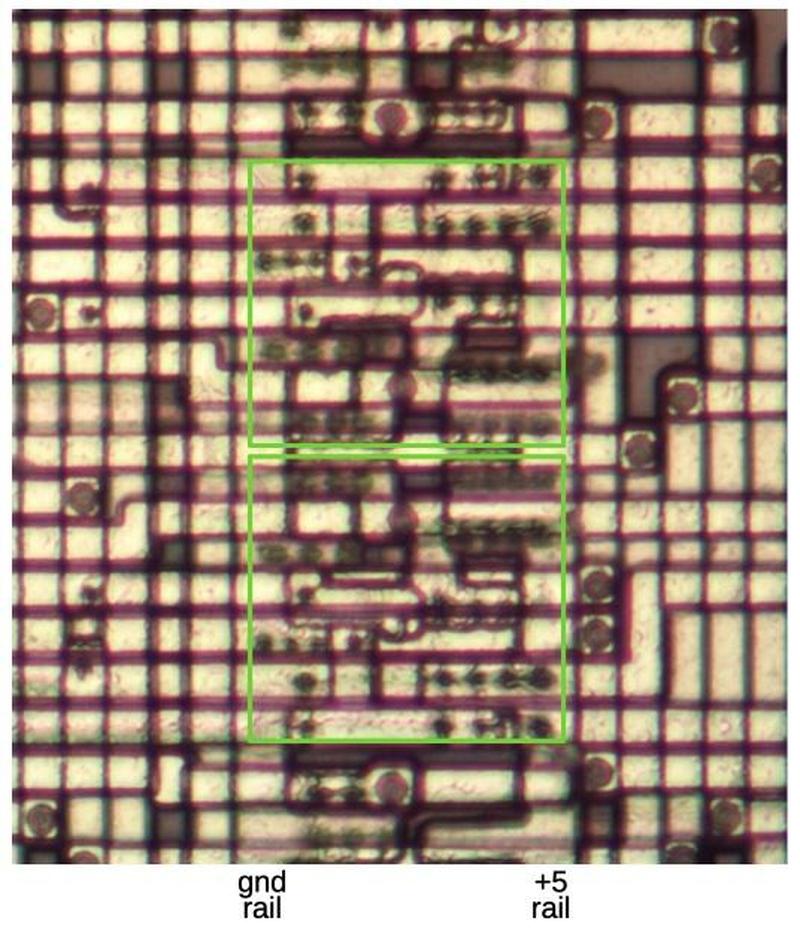
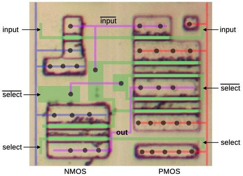
One interesting feature is the layout of the large AND gates. A 6-input AND gate is a large device, difficult to fit into one cell of the incrementer. The solution is that the gate is spread out across multiple cells. Specifically, the gate uses a standard CMOS NAND gate circuit with NMOS transistors in series and PMOS transistors in parallel. Each cell has an NMOS transistor and a PMOS transistor, and the chains are connected at the end to form the desired NAND gate. (Inverting the output produces the desired AND function.) This spread-out layout technique is unusual, but keeps each bit's circuitry approximately the same size.

The incrementer circuitry was tricky to reverse engineer because of these techniques. In particular, most of the prefetcher consists of a single block of circuitry repeated 32 times, once for each bit. The incrementer, on the other hand, consists of four different blocks of circuitry, repeating in an irregular pattern. Specifically, one block starts a carry chain, a second block continues the carry chain, and a third block ends a carry chain. The block before the ending block is different (one large transistor to drive the last block), making four variants in total. This irregular pattern is visible in the earlier photo of the prefetcher.

The alignment network

The bottom part of the prefetcher rotates data to align it as needed. Unlike some processors, the x86 does not enforce aligned memory accesses. That is, a 32-bit value does not need to start on a 4-byte boundary in memory. As a result, a 32-bit value may be split across two 32-bit rows of the prefetch queue. Moreover, when the instruction decoder fetches one byte of an instruction, that byte may be at any position in the prefetch queue.

To deal with these problems, the prefetcher includes an alignment network that can rotate bytes to output a byte, word, or four bytes with the alignment required by the rest of the processor.

The diagram below shows part of this alignment network. Each bit exiting the prefetch queue (top) has four wires, for rotates of 24, 16, 8, or 0 bits. Each rotate wire is connected to one of the 32 horizontal bit lines. Finally, each horizontal bit line has an output tap, going to the datapath below. (The vertical lines are in the chip's lower M1 metal layer, while the horizontal lines are in the upper M2 metal layer. For this photo, I removed the M2 layer to show the underlying layer. Shadows of the original horizontal lines are still visible.)

Part of the alignment network.

Part of the alignment network.

The idea is that by selecting one set of vertical rotate lines, the 32-bit output from the prefetch queue will be rotated left by that amount. For instance, to rotate by 8, bits are sent down the "rotate 8" lines. Bit 0 from the prefetch queue will energize horizontal line 8, bit 1 will energize horizontal line 9, and so forth, with bit 31 wrapping around to horizontal line 7. Since horizontal bit line 8 is connected to output 8, the result is that bit 0 is output as bit 8, bit 1 is output as bit 9, and so forth.

The four possibilities for aligning a 32-bit value. The four bytes above are shifted as specified to produce the desired output below.

The four possibilities for aligning a 32-bit value. The four bytes above are shifted as specified to produce the desired output below.

For the alignment process, one 32-bit output may be split across two 32-bit entries in the prefetch queue in four different ways, as shown above. These combinations are implemented by multiplexers and drivers. Two 32-bit multiplexers select the two relevant rows in the prefetch queue (blue and green above). Four 32-bit drivers are connected to the four sets of vertical lines, with one set of drivers activated to produce the desired shift. Each byte of each driver is wired to achieve the alignment shown above. For instance, the rotate-8 driver gets its top byte from the "green" multiplexer and the other three bytes from the "blue" multiplexer. The result is that the four bytes, split across two queue rows, are rotated to form an aligned 32-bit value.

Sign extension

The final circuit is sign extension. Suppose you want to add an 8-bit value to a 32-bit value. An unsigned 8-bit value can be extended to 32 bits by simply filling the upper bits with zeroes. But for a signed value, it's trickier. For instance, -1 is the eight-bit value 0xFF, but the 32-bit value is 0xFFFFFFFF. To convert an 8-bit signed value to 32 bits, the top 24 bits must be filled in with the top bit of the original value (which indicates the sign). In other words, for a positive value, the extra bits are filled with 0, but for a negative value, the extra bits are filled with 1. This process is called sign extension.9

In the 386, a circuit at the bottom of the prefetcher performs sign extension for values in instructions. This circuit supports extending an 8-bit value to 16 bits or 32 bits, as well as extending a 16-bit value to 32 bits. This circuit will extend a value with zeros or with the sign, depending on the instruction.

The schematic below shows one bit of this sign extension circuit. It consists of a latch on the left and right, with a multiplexer in the middle. The latches are constructed with a standard 386 circuit using a CMOS switch (see footnote).7 The multiplexer selects one of three values: the bit value from the swap network, 0 for sign extension, or 1 for sign extension. The multiplexer is constructed from a CMOS switch if the bit value is selected and two transistors for the 0 or 1 values. This circuit is replicated 32 times, although the bottom byte only has the latches, not the multiplexer, as sign extension does not modify the bottom byte.

The sign extend circuit associated with bits 31-8 from the prefetcher.

The sign extend circuit associated with bits 31-8 from the prefetcher.

The second part of the sign extension circuitry determines if the bits should be filled with 0 or 1 and sends the control signals to the circuit above. The gates on the left determine if the sign extension bit should be a 0 or a 1. For a 16-bit sign extension, this bit comes from bit 15 of the data, while for an 8-bit sign extension, the bit comes from bit 7. The four gates on the right generate the signals to sign extend each bit, producing separate signals for the bit range 31-16 and the range 15-8.

This circuit determines which bits should be filled with 0 or 1.

This circuit determines which bits should be filled with 0 or 1.

The layout of this circuit on the die is somewhat unusual. Most of the prefetcher circuitry consists of 32 identical columns, one for each bit.8 The circuitry above is implemented once, using about 16 gates (buffers and inverters are not shown above). Despite this, the circuitry above is crammed into bit positions 17 through 7, creating irregularities in the layout. Moreover, the implementation of the circuitry in silicon is unusual compared to the rest of the 386. Most of the 386's circuitry uses the two metal layers for interconnection, minimizing the use of polysilicon wiring. However, the circuit above also uses long stretches of polysilicon to connect the gates.

Layout of the sign extension circuitry. This circuitry is at the bottom of the prefetch queue.

Layout of the sign extension circuitry. This circuitry is at the bottom of the prefetch queue.

The diagram above shows the irregular layout of the sign extension circuitry amid the regular datapath circuitry that is 32 bits wide. The sign extension circuitry is shown in green; this is the circuitry described at the top of this section, repeated for each bit 31-8. The circuitry for bits 15-8 has been shifted upward, perhaps to make room for the sign extension control circuitry, indicated in red. Note that the layout of the control circuitry is completely irregular, since there is one copy of the circuitry and it has no internal structure. One consequence of this layout is the wasted space to the left and right of this circuitry block, the tan regions with no circuitry except vertical metal lines passing through. At the far right, a block of circuitry to control the latches has been wedged under bit 0. Intel's designers go to great effort to minimize the size of the processor die since a smaller die saves substantial money. This layout must have been the most efficient they could manage, but I find it aesthetically displeasing compared to the regularity of the rest of the datapath.

How instructions flow through the chip

Instructions follow a tortuous path through the 386 chip. First, the Bus Interface Unit in the upper right corner reads instructions from memory and sends them over a 32-bit bus (blue) to the prefetch unit. The prefetch unit stores the instructions in the 16-byte prefetch queue.

Instructions follow a twisting path to and from the prefetch queue.

Instructions follow a twisting path to and from the prefetch queue.

How is an instruction executed from the prefetch queue? It turns out that there are two distinct paths. Suppose you're executing an instruction to add 12345678 to the EAX register. The prefetch queue will hold the five bytes 05 (the opcode), 78, 56, 34, and 12. The prefetch queue provides opcodes to the decoder one byte at a time over the 8-bit bus shown in red. The bus takes the lowest 8 bits from the prefetch queue's alignment network and sends this byte to a buffer (the small square at the head of the red arrow). From there, the opcode travels to the instruction decoder.10 The instruction decoder, in turn, uses large tables (PLAs) to convert the x86 instruction into a 111-bit internal format with 19 different fields.11

The data bytes of an instruction, on the other hand, go from the prefetch queue to the ALU (Arithmetic Logic Unit) through a 32-bit data bus (orange). Unlike the previous buses, this data bus is spread out, with one wire through each column of the datapath. This bus extends through the entire datapath so values can also be stored into registers. For instance, the MOV (move) instruction can store a value from an instruction (an "immediate" value) into a register.

Conclusions

The 386's prefetch queue contains about 7400 transistors, more than an Intel 8080 processor. (And this is just the queue itself; I'm ignoring the prefetch control logic.) This illustrates the rapid advance of processor technology: part of one functional unit in the 386 contains more transistors than an entire 8080 processor from 11 years earlier. And this unit is less than 3% of the entire 386 processor.

Every time I look at an x86 circuit, I see the complexity required to support backward compatibility, and I gain more understanding of why RISC became popular. The prefetcher is no exception. Much of the complexity is due to the 386's support for unaligned memory accesses, requiring a byte shift network to move bytes into 32-bit alignment. Moreover, at the other end of the instruction bus is the complicated instruction decoder that decodes intricate x86 instructions. Decoding RISC instructions is much easier.

In any case, I hope you've found this look at the prefetch circuitry interesting. I plan to write more about the 386, so follow me on Bluesky (@righto.com) or RSS for updates. I've written multiple articles on the 386 previously; a good place to start might be my survey of the 368 dies.

Footnotes and references

  1. The width of the circuitry for one bit changes a few times: while the prefetch queue and segment descriptor cache use a circuit that is 66 µm wide, the datapath circuitry is a bit tighter at 60 µm. The barrel shifter is even narrower at 54.5 µm per bit. Connecting circuits with different widths wastes space, since the wiring to connect the bits requires horizontal segments to adjust the spacing. But it also wastes space to use widths that are wider than needed. Thus, changes in the spacing are rare, where the tradeoffs make it worthwhile. 

  2. The Intel 8086 processor had a six-byte prefetch queue, while the Intel 8088 (used in the original IBM PC) had a prefetch queue of just four bytes. In comparison, the 16-byte queue of the 386 seems luxurious. (Some 386 processors, however, are said to only use 12 bytes due to a bug.)

    The prefetch queue assumes instructions are executed in linear order, so it doesn't help with branches or loops. If the processor encounters a branch, the prefetch queue is discarded. (In contrast, a modern cache will work even if execution jumps around.) Moreover, the prefetch queue doesn't handle self-modifying code. (It used to be common for code to change itself while executing to squeeze out extra performance.) By loading code into the prefetch queue and then modifying instructions, you could determine the size of the prefetch queue: if the old instruction was executed, it must be in the prefetch queue, but if the modified instruction was executed, it must be outside the prefetch queue. Starting with the Pentium Pro, x86 processors flush the prefetch queue if a write modifies a prefetched instruction. 

  3. The prefetch unit generates "linear" addresses that must be translated to physical addresses by the paging unit (ref). 

  4. I don't know which phase of the clock is phase 1 and which is phase 2, so I've assigned the numbers arbitrarily. The 386 creates four clock signals internally from a clock input CLK2 that runs at twice the processor's clock speed. The 386 generates a two-phase clock with non-overlapping phases. That is, there is a small gap between when the first phase is high and when the second phase is high. The 386's circuitry is controlled by the clock, with alternate blocks controlled by alternate phases. Since the clock phases don't overlap, this ensures that logic blocks are activated in sequence, allowing the orderly flow of data. But because the 386 uses CMOS, it also needs active-low clocks for the PMOS transistors. You might think that you could simply use the phase 1 clock as the active-low phase 2 clock and vice versa. The problem is that these clock phases overlap when used as active-low; there are times when both clock signals are low. Thus, the two clock phases must be explicitly inverted to produce the two active-low clock phases. I described the 386's clock generation circuitry in detail in this article

  5. The Manchester carry chain is typically used in an adder, which makes it more complicated than shown here. In particular, a new carry can be generated when two 1 bits are added. Since we're looking at an incrementer, this case can be ignored.

    The Manchester carry chain was first described in Parallel addition in digital computers: a new fast ‘carry’ circuit. It was developed at the University of Manchester in 1959 and used in the Atlas supercomputer. 

  6. For some reason, the incrementer uses a completely different XOR circuit from the comparator, built from a multiplexer instead of logic. In the circuit below, the two CMOS switches form a multiplexer: if the first input is 1, the top switch turns on, while if the first input is a 0, the bottom switch turns on. Thus, if the first input is a 1, the second input passes through and then is inverted to form the output. But if the first input is a 0, the second input is inverted before the switch and then is inverted again to form the output. Thus, the second input is inverted if the first input is 1, which is a description of XOR.

    The implementation of an XOR gate in the incrementer.

    The implementation of an XOR gate in the incrementer.

    I don't see any clear reason why two different XOR circuits were used in different parts of the prefetcher. Perhaps the available space for the layout made a difference. Or maybe the different circuits have different timing or output current characteristics. Or it could just be the personal preference of the designers. 

  7. The latch circuit is based on a CMOS switch (or transmission gate) and a weak inverter. Normally, the inverter loop holds the bit. However, if the CMOS switch is enabled, its output overpowers the signal from the weak inverter, forcing the inverter loop into the desired state.

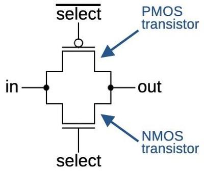
    The CMOS switch consists of an NMOS transistor and a PMOS transistor in parallel. By setting the top control input high and the bottom control input low, both transistors turn on, allowing the signal to pass through the switch. Conversely, by setting the top input low and the bottom input high, both transistors turn off, blocking the signal. CMOS switches are used extensively in the 386, to form multiplexers, create latches, and implement XOR. 

  8. Most of the 386's control circuitry is to the right of the datapath, rather than awkwardly wedged into the datapath. So why is this circuit different? My hypothesis is that since the circuit needs the values of bit 15 and bit 7, it made sense to put the circuitry next to bits 15 and 7; if this control circuitry were off to the right, long wires would need to run from bits 15 and 7 to the circuitry. 

  9. In case this post is getting tedious, I'll provide a lighter footnote on sign extension. The obvious mnemonic for a sign extension instruction is SEX, but that mnemonic was too risque for Intel. The Motorola 6809 processor (1978) used this mnemonic, as did the related 68HC12 microcontroller (1996). However, Steve Morse, architect of the 8086, stated that the sign extension instructions on the 8086 were initially named SEX but were renamed before release to the more conservative CBW and CWD (Convert Byte to Word and Convert Word to Double word).

    The DEC PDP-11 was a bit contradictory. It has a sign extend instruction with the mnemonic SXT; the Jargon File claims that DEC engineers almost got SEX as the assembler mnemonic, but marketing forced the change. On the other hand, SEX was the official abbreviation for Sign Extend (see PDP-11 Conventions Manual, PDP-11 Paper Tape Software Handbook) and SEX was used in the microcode for sign extend.

    RCA's CDP1802 processor (1976) may have been the first with a SEX instruction, using the mnemonic SEX for the unrelated Set X instruction. See also this Retrocomputing Stack Exchange page

  10. It seems inconvenient to send instructions all the way across the chip from the Bus Interface Unit to the prefetch queue and then back across to the chip to the instruction decoder, which is next to the Bus Interface Unit. But this was probably the best alternative for the layout, since you can't put everything close to everything. The 32-bit datapath circuitry is on the left, organized into 32 columns. It would be nice to put the Bus Interface Unit other there too, but there isn't room, so you end up with the wide 32-bit data bus going across the chip. Sending instruction bytes across the chip is less of an impact, since the instruction bus is just 8 bits wide. 

  11. See "Performance Optimizations of the 80386", Slager, Oct 1986, in Proceedings of ICCD, pages 165-168. 

The absurdly complicated circuitry for the 386 processor's registers

The groundbreaking Intel 386 processor (1985) was the first 32-bit processor in the x86 architecture. Like most processors, the 386 contains numerous registers; registers are a key part of a processor because they provide storage that is much faster than main memory. The register set of the 386 includes general-purpose registers, index registers, and segment selectors, as well as registers with special functions for memory management and operating system implementation. In this blog post, I look at the silicon die of the 386 and explain how the processor implements its main registers.

It turns out that the circuitry that implements the 386's registers is much more complicated than one would expect. For the 30 registers that I examine, instead of using a standard circuit, the 386 uses six different circuits, each one optimized for the particular characteristics of the register. For some registers, Intel squeezes register cells together to double the storage capacity. Other registers support accesses of 8, 16, or 32 bits at a time. Much of the register file is "triple-ported", allowing two registers to be read simultaneously while a value is written to a third register. Finally, I was surprised to find that registers don't store bits in order: the lower 16 bits of each register are interleaved, while the upper 16 bits are stored linearly.

The photo below shows the 386's shiny fingernail-sized silicon die under a special metallurgical microscope. I've labeled the main functional blocks. For this post, the Data Unit in the lower left quadrant of the chip is the relevant component. It consists of the 32-bit arithmetic logic unit (ALU) along with the processor's main register bank (highlighted in red at the bottom). The circuitry, called the datapath, can be viewed as the heart of the processor.

This die photo of the 386 shows the location of the registers. Click this image (or any other) for a larger version.

This die photo of the 386 shows the location of the registers. Click this image (or any other) for a larger version.

The datapath is built with a regular structure: each register or ALU functional unit is a horizontal stripe of circuitry, forming the horizontal bands visible in the image. For the most part, this circuitry consists of a carefully optimized circuit copied 32 times, once for each bit of the processor. Each circuit for one bit is exactly the same width—60 µm—so the functional blocks can be stacked together like microscopic LEGO bricks. To link these circuits, metal bus lines run vertically through the datapath in groups of 32, allowing data to flow up and down through the blocks. Meanwhile, control lines run horizontally, enabling ALU operations or register reads and writes; the irregular circuitry on the right side of the Data Unit produces the signals for these control lines, activating the appropriate control lines for each instruction.

The datapath is highly structured to maximize performance while minimizing its area on the die. Below, I'll look at how the registers are implemented according to this structure.

The 386's registers

A processor's registers are one of the most visible features of the processor architecture. The 386 processor contains 16 registers for use by application programmers, a small number by modern standards, but large enough for the time. The diagram below shows the eight 32-bit general-purpose registers. At the top are four registers called EAX, EBX, ECX, and EDX. Although these registers are 32-bit registers, they can also be treated as 16 or 8-bit registers for backward compatibility with earlier processors. For instance, the lower half of EAX can be accessed as the 16-bit register AX, while the bottom byte of EAX can be accessed as the 8-bit register AL. Moreover, bits 15-8 can also be accessed as an 8-bit register called AH. In other words, there are four different ways to access the EAX register, and similarly for the other three registers. As will be seen, these features complicate the implementation of the register set.

The general purpose registers in the 386. From 80386 Programmer's Reference Manual, page 2-8.

The general purpose registers in the 386. From 80386 Programmer's Reference Manual, page 2-8.

The bottom half of the diagram shows that the 32-bit EBP, ESI, EDI, and ESP registers can also be treated as 16-bit registers BP, SI, DI, and SP. Unlike the previous registers, these ones cannot be treated as 8-bit registers. The 386 also has six segment registers that define the start of memory segments; these are 16-bit registers. The 16 application registers are rounded out by the status flags and instruction pointer (EIP); they are viewed as 32-bit registers, but their implementation is more complicated. The 386 also has numerous registers for operating system programming, but I won't discuss them here, since they are likely in other parts of the chip.1 Finally, the 386 has numerous temporary registers that are not visible to the programmer but are used by the microcode to perform complex instructions.

The 6T and 8T static RAM cells

The 386's registers are implemented with static RAM cells, a circuit that can hold one bit. These cells are arranged into a grid to provide multiple registers. Static RAM can be contrasted with the dynamic RAM that computers use for their main memory: dynamic RAM holds each bit in a tiny capacitor, while static RAM uses a faster but larger and more complicated circuit. Since main memory holds gigabytes of data, it uses dynamic RAM to provide dense and inexpensive storage. But the tradeoffs are different for registers: the storage capacity is small, but speed is of the essence. Thus, registers use the static RAM circuit that I'll explain below.

The concept behind a static RAM cell is to connect two inverters into a loop. If an inverter has a "0" as input, it will output a "1", and vice versa. Thus, the inverter loop will be stable, with one inverter on and one inverter off, and each inverter supporting the other. Depending on which inverter is on, the circuit stores a 0 or a 1, as shown below. Thus, the pair of inverters provides one bit of memory.

Two inverters in a loop can store a 0 or a 1.

Two inverters in a loop can store a 0 or a 1.

To be useful, however, the inverter loop needs a way to store a bit into it, as well as a way to read out the stored bit. To write a new value into the circuit, two signals are fed in, forcing the inverters to the desired new values. One inverter receives the new bit value, while the other inverter receives the complemented bit value. This may seem like a brute-force way to update the bit, but it works. The trick is that the inverters in the cell are small and weak, while the input signals are higher current, able to overpower the inverters.2 These signals are fed in through wiring called "bitlines"; the bitlines can also be used to read the value stored in the cell.

By adding two pass transistors to the circuit, the cell can be read and written.

By adding two pass transistors to the circuit, the cell can be read and written.

To control access to the register, the bitlines are connected to the inverters through pass transistors, which act as switches to control access to the inverter loop.3 When the pass transistors are on, the signals on the write lines can pass through to the inverters. But when the pass transistors are off, the inverters are isolated from the write lines. The pass transistors are turned on by a control signal, called a "wordline" since it controls access to a word of storage in the register. Since each inverter is constructed from two transistors, the circuit above consists of six transistors—thus this circuit is called a "6T" cell.

The 6T cell uses the same bitlines for reading and writing, so you can't read and write to registers simultaneously. But adding two transistors creates an "8T" circuit that lets you read from one register and write to another register at the same time. (In technical terms, the register file is two-ported.) In the 8T schematic below, the two additional transistors (G and H) are used for reading. Transistor G buffers the cell's value; it turns on if the inverter output is high, pulling the read output bitline low.4 Transistor H is a pass transistor that blocks this signal until a read is performed on this register; it is controlled by a read wordline. Note that there are two bitlines for writing (as before) along with one bitline for reading.

Schematic of a storage cell. Each transistor is labeled with a letter.

Schematic of a storage cell. Each transistor is labeled with a letter.

To construct registers (or memory), a grid is constructed from these cells. Each row corresponds to a register, while each column corresponds to a bit position. The horizontal lines are the wordlines, selecting which word to access, while the vertical lines are the bitlines, passing bits in or out of the registers. For a write, the vertical bitlines provide the 32 bits (along with their complements). For a read, the vertical bitlines receive the 32 bits from the register. A wordline is activated to read or write the selected register. To summarize: each row is a register, data flows vertically, and control signals flow horizontally.

Static memory cells (8T) organized into a grid.

Static memory cells (8T) organized into a grid.

Six register circuits in the 386

The die photo below zooms in on the register circuitry in the lower left corner of the 386 processor. You can see the arrangement of storage cells into a grid, but note that the pattern changes from row to row. This circuitry implements 30 registers: 22 of the registers hold 32 bits, while the bottom ones are 16-bit registers. By studying the die, I determined that there are six different register circuits, which I've arbitrarily labeled (a) to (f). In this section, I'll describe these six types of registers.

The 386's main register bank, at the bottom of the datapath.  The numbers show how many bits of the register can be accessed.

The 386's main register bank, at the bottom of the datapath. The numbers show how many bits of the register can be accessed.

I'll start at the bottom with the simplest circuit: eight 16-bit registers that I'm calling type (f). You can see a "notch" on the left side of the register file because these registers are half the width of the other registers (16 bits versus 32 bits). These registers are implemented with the 8T circuit described earlier, making them dual ported: one register can be read while another register is written. As described earlier, three vertical bus lines pass through each bit: one bitline for reading and two bitlines (with opposite polarity) for writing. Each register has two control lines (wordlines): one to select a register for reading and another to select a register for writing.

The photo below shows how four cells of type (f) are implemented on the chip. In this image, the chip's two metal layers have been removed along with most of the polysilicon wiring, showing the underlying silicon. The dark outlines indicate regions of doped silicon, while the stripes across the doped region correspond to transistor gates. I've labeled each transistor with a letter corresponding to the earlier schematic. Observe that the layout of the bottom half is a mirrored copy of the upper half, saving a bit of space. The left and right sides are approximately mirrored; the irregular shape allows separate read and wite wordlines to control the left and right halves without colliding.

Four memory cells of type (f), separated by dotted lines. The small irregular squares are remnants of polysilicon
that weren't fully removed.

Four memory cells of type (f), separated by dotted lines. The small irregular squares are remnants of polysilicon that weren't fully removed.

The 386's register file and datapath are designed with 60 µm of width assigned to each bit. However, the register circuit above is unusual: the image above is 60 µm wide but there are two register cells side-by-side. That is, the circuit crams two bits in 60 µm of width, rather than one. Thus, this dense layout implements two registers per row (with interleaved bits), providing twice the density of the other register circuits.

If you're curious to know how the transistors above are connected, the schematic below shows how the physical arrangement of the transistors above corresponds to two of the 8T memory cells described earlier. Since the 386 has two overlapping layers of metal, it is very hard to interpret a die photo with the metal layers. But see my earlier article if you want these photos.

Schematic of two static cells in the 386, labeled "R" and "L" for "right" and "left". The schematic approximately matches the physical layout.

Schematic of two static cells in the 386, labeled "R" and "L" for "right" and "left". The schematic approximately matches the physical layout.

Above the type (f) registers are 10 registers of type (e), occupying five rows of cells. These registers are the same 8T implementation as before, but these registers are 32 bits wide instead of 16. Thus, the register takes up the full width of the datapath, unlike the previous registers. As before, the double-density circuit implements two registers per row. The silicon layout is identical (apart from being 32 bits wide instead of 16), so I'm not including a photo.

Above those registers are four (d) registers, which are more complex. They are triple-ported registers, so one register can be written while two other registers are read. (This is useful for ALU operations, for instance, since two values can be added and the result written back at the same time.) To support reading a second register, another vertical bus line is added for each bit. Each cell has two more transistors to connect the cell to the new bitline. Another wordline controls the additional read path. Since each cell has two more transistors, there are 10 transistors in total and the circuit is called 10T.

Four cells of type (d). The striped green regions are the remnants of oxide layers that weren't completely removed, and can be ignored.

Four cells of type (d). The striped green regions are the remnants of oxide layers that weren't completely removed, and can be ignored.

The diagram above shows four memory cells of type (d). Each of these cells takes the full 60 µm of width, unlike the previous double-density cells. The cells are mirrored horizontally and vertically; this increases the density slightly since power lines can be shared between cells. I've labeled the transistors A through H as before, as well as the two additional transistors I and J for the second read line. The circuit is the same as before, except for the two additional transistors, but the silicon layout is significantly different.

Each of the (d) registers has five control lines. Two control lines select a register for reading, connecting the register to one of the two vertical read buses. The three write lines allow parts of the register to be written independently: the top 16 bits, the next 8 bits, or the bottom 8 bits. This is required by the x86 architecture, where a 32-bit register such as EAX can also be accessed as the 16-bit AX register, the 8-bit AH register, or the 8-bit AL register. Note that reading part of a register doesn't require separate control lines: the register provides all 32 bits and the reading circuit can ignore the bits it doesn't want.

Proceeding upward, the three (c) registers have a similar 10T implementation. These registers, however, do not support partial writes so all 32 bits must be written at once. As a result, these registers only require three control lines (two for reads and one for writes). With fewer control lines, the cells can be fit into less vertical space, so the layout is slightly more compact than the previous type (d) cells. The diagram below shows four type (c) rows above two type (d) rows. Although the cells have the same ten transistors, they have been shifted around somewhat.

Four rows of type (c) above two cells of type (d).

Four rows of type (c) above two cells of type (d).

Next are the four (b) registers, which support 16-bit writes and 32-bit writes (but not 8-bit writes). Thus, these registers have four control lines (two for reads and two for writes). The cells take slightly more vertical space than the (c) cells due to the additional control line, but the layout is almost identical.

Finally, the (a) register at the top has an unusual feature: it can receive a copy of the value in the register just below it. This value is copied directly between the registers, without using the read or write buses. This register has 3 control lines: one for read, one for write, and one for copying.

A cell of type (a), which can copy the value in the cell of type (b) below.

A cell of type (a), which can copy the value in the cell of type (b) below.

The diagram above shows a cell of type (a) above a cell of type (b). The cell of type (a) is based on the standard 8T circuit, but with six additional transistors to copy the value of the cell below. Specifically, two inverters buffer the output from cell (b), one inverter for each side of the cell. These inverters are implemented with transistors I1 through I4.5 Two transistors, S1 and S2, act as a pass-transistor switches between these inverters and the memory cell. When activated by the control line, the switch transistors allow the inverters to overwrite the memory cell with the contents of the cell below. Note that cell (a) takes considerably more vertical space because of the extra transistors.

Speculation on the physical layout of the registers

I haven't determined the mapping between the 386's registers and the 30 physical registers, but I can speculate. First, the 386 has four registers that can be accessed as 8, 16, or 32-bit registers: EAX, EBX, ECX, and EDX. These must map onto the (d) registers, which support these access patterns.

The four index registers (ESP, EBP, ESI, and EDI) can be used as 32-bit registers or 16-bit registers, matching the four (b) registers with the same properties. Which one of these registers can be copied to the type (a) register? Maybe the stack pointer (ESP) is copied as part of interrupt handling.

The register file has eight 16-bit registers, type (f). Since there are six 16-bit segment registers in the 386, I suspect the 16-bit registers are the segment registers and two additional registers. The LOADALL instruction gives some clues, suggesting that the two additional 16-bit registers are LDT (Local Descriptor Table register) and TR (Task Register). Moreover, LOADALL handles 10 temporary registers, matching the 10 registers of type (e) near the bottom of the register file. The three 32-bit registers of type (c) may be the CR0 control register and the DR6 and DR7 debug registers.

The six 16-bit segment registers in the 386.

The six 16-bit segment registers in the 386.

In this article, I'm only looking at the main register file in the datapath. The 386 presumably has other registers scattered around the chip for various purposes. For instance, the Segment Descriptor Cache contains multiple registers similar to type (e), probably holding cache entries. The processor status flags and the instruction pointer (EIP) may not be implemented as discrete registers.6

To the right of the register file, a complicated block of circuitry uses seven-bit values to select registers. Two values select the registers (or constants) to read, while a third value selects the register to write. I'm currently analyzing this circuitry, which should provide more insight into how the physical registers are assigned.

The shuffle network

There's one additional complication in the register layout. As mentioned earlier, the bottom 16 bits of the main registers can be treated as two 8-bit registers.7 For example, the 8-bit AH and AL registers form the bottom 16 bits of the EAX register. I explained earlier how the registers use multiple write control lines to allow these different parts of the register to be updated separately. However, there is also a layout problem.

To see the problem, suppose you perform an 8-bit ALU operation on the AH register, which is bits 15-8 of the EAX register. These bits must be shifted down to positions 7-0 so they can take part in the ALU operation, and then must be shifted back to positions 15-8 when stored into AH. On the other hand, if you perform an ALU operation on AL (bits 7-0 of EAX), the bits are already in position and don't need to be shifted.

To support the shifting required for 8-bit register operations, the 386's register file physically interleaves the bits of the two lower bytes (but not the high bytes). As a result, bit 0 of AL is next to bit 0 of AH in the register file, and so forth. This allows multiplexers to easily select bits from AH or AL as needed. In other words, each bit of AH and AL is in almost the correct physical position, so an 8-bit shift is not required. (If the bits were in order, each multiplexer would need to be connected to bits that are separated by eight positions, requiring inconvenient wiring.)8

The shuffle network above the register file interleaves the bottom 16 bits.

The shuffle network above the register file interleaves the bottom 16 bits.

The photo above shows the shuffle network. Each bit has three bus lines associated with it: two for reads and one for writes, and these all get shuffled. On the left, the lines for the 16 bits pass straight through. On the right, though, the two bytes are interleaved. This shuffle network is located below the ALU and above the register file, so data words are shuffled when stored in the register file and then unshuffled when read from the register file.9

In the photo, the lines on the left aren't quite straight. The reason is that the circuitry above is narrower than the circuitry below. For the most part, each functional block in the datapath is constructed with the same width (60 µm) for each bit. This makes the layout simpler since functional blocks can be stacked on top of each other and the vertical bus wiring can pass straight through. However, the circuitry above the registers (for the barrel shifter) is about 10% narrower (54.5 µm), so the wiring needs to squeeze in and then expand back out.10 There's a tradeoff of requiring more space for this wiring versus the space saved by making the barrel shifter narrower and Intel must have considered the tradeoff worthwhile. (My hypothesis is that since the shuffle network required additional wiring to shuffle the bits, it didn't take up more space to squeeze the wiring together at the same time.)

Conclusions

If you look in a book on processor design, you'll find a description of how registers can be created from static memory cells. However, the 386 illustrates that the implementation in a real processor is considerably more complicated. Instead of using one circuit, Intel used six different circuits for the registers in the 386.

The 386's register circuitry also shows the curse of backward compatibility. The x86 architecture supports 8-bit register accesses for compatibility with processors dating back to 1971. This compatibility requires additional circuitry such as the shuffle network and interleaved registers. Looking at the circuitry of x86 processors makes me appreciate some of the advantages of RISC processors, which avoid much of the ad hoc circuitry of x86 processors.

If you want more information about how the 386's memory cells were implemented, I wrote a lower-level article earlier. I plan to write more about the 386, so follow me on Bluesky (@righto.com) or RSS for updates.

Footnotes and references

  1. The 386 has multiple registers that are only relevant to operating systems programmers (see Chapter 4 of the 386 Programmer's Reference Manual). These include the Global Descriptor Table Register (GDTR), Local Descriptor Table Register (LDTR), Interrupt Descriptor Table Register (IDTR), and Task Register (TR). There are four Control Registers CR0-CR3; CR0 controls coprocessor usage, paging, and a few other things. The six Debug Registers for hardware breakpoints are named DR0-DR3, DR6, and DR7. The two Test Registers for TLB testing are named TR6 and TR7. I expect that these registers are in the 386's Segment Unit and Paging Unit, rather than part of the processing datapath. 

  2. Typically the write driver circuit generates a strong low on one of the bitlines, flipping the corresponding inverter to a high output. As soon as one inverter flips, it will force the other inverter into the right state. To support this, the pullup transistors in the inverters are weaker than normal. 

  3. The pass transistor passes its signal through or blocks it. In CMOS, this is usually implemented with a transmission gate with an NMOS and a PMOS transistor in parallel. The cell uses only the NMOS transistor, which is much worse at passing a high signal than a low signal. Because there is one NMOS pass transistor on each side of the inverters, one of the transistors will be passing a low signal that will flip the state. 

  4. The bitline is typically precharged to a high level for a read, and then the cell pulls the line low for a 0. This is more compact than including circuitry in each cell to pull the line high. 

  5. Note that buffering is needed so the (b) cell can write to the (a) cell. If the cells were connected directly, cell (a) could overwrite cell (b) as easily as cell (b) could overwrite cell (a). With the inverters in between, cell (b) won't be affected by cell (a). 

  6. In the 8086, the processor status flags are not stored as a physical register, but instead consist of flip-flops scattered throughout the chip (details). The 386 probably has a similar implementation for the flags.

    In the 8086, the program counter (instruction pointer) does not exist as such. Instead, the instruction prefetch circuitry has a register holding the current prefetch address. If the program counter address is required (to push a return address or to perform a relative branch, for instance), the program counter value is derived from the prefetch address. If the 386 is similar, the program counter won't have a physical register in the register file. 

  7. The x86 architecture combines two 8-bit registers to form a 16-bit register for historical reasons. The TTL-based Datapoint 2200 (1971) system had 8-bit A, B, C, D, E, H, and L registers, with the H and L registers combined to form a 16-bit indexing register for memory accesses. Intel created a microprocessor version of the Datapoint 2200's architecture, called the 8008. Intel's 8080 processor extended the register pairs so BC and DE could also be used as 16-bit registers. The 8086 kept this register design, but changed the 16-bit register names to AX, BX, CX, and DX, with the 8-bit parts called AH, AL, and so forth. Thus, the unusual physical structure of the 386's register file is due to compatibility with a programmable terminal from 1971. 

  8. To support 8-bit and 16-bit operations, the 8086 processor used a similar interleaving scheme with the two 8-bit halves of a register interleaved. Since the 8086 was a 16-bit processor, though, its interleaving was simpler than the 32-bit 386. Specifically, the 8086 didn't have the upper 16 bits to deal with. 

  9. The 386's constant ROM is located below the shuffle network. Thus, constants are stored with the bits interleaved in order to produce the right results. (This made the ROM contents incomprehensible until I figured out the shuffling pattern, but that's a topic for another article.) 

  10. The main body of the datapath (ALU, etc.) has the same 60 µm cell width as the register file. However, the datapath is slightly wider than the register file overall. The reason? The datapath has a small amount of circuitry between bits 7 and 8 and between bits 15 and 16, in order to handle 8-bit and 16-bit operations. As a result, the logical structure of the registers is visible as stripes in the physical layout of the ALU below. (These stripes are also visible in the die photo at the beginning of this article.)

    Part of the ALU circuitry, displayed underneath the structure of the EAX register.

    Part of the ALU circuitry, displayed underneath the structure of the EAX register.


A tricky Commodore PET repair: tracking down 6 1/2 bad chips

mult3

In 1977, Commodore released the PET computer, a quirky home computer that combined the processor, a tiny keyboard, a cassette drive for storage, and a trapezoidal screen in a metal unit. The Commodore PET, the Apple II, and Radio Shack's TRS-80 started the home computer market with ready-to-run computers, systems that were called in retrospect the 1977 Trinity. I did much of my early programming on the PET, so when someone offered me a non-working PET a few years ago, I took it for nostalgic reasons.

You'd think that a home computer would be easy to repair, but it turned out to be a challenge. The chips in early PETs are notorious for failures and, sure enough, we found multiple bad chips. Moreover, these RAM and ROM chips were special designs that are mostly unobtainable now. In this post, I'll summarize how we repaired the system, in case it helps anyone else.

When I first powered up the computer, I was greeted with a display full of random characters. This was actually reassuring since it showed that most of the computer was working: not just the monitor, but the video RAM, character ROM, system clock, and power supply were all operational.

The Commodore PET started up, but the screen was full of garbage.

The Commodore PET started up, but the screen was full of garbage.

With an oscilloscope, I examined signals on the system bus and found that the clock, address, and data lines were full of activity, so the 6502 CPU seemed to be operating. However, some of the data lines had three voltage levels, as shown below. This was clearly not good, and suggested that a chip on the bus was messing up the data signals.

The scope shows three voltage levels on the data bus.

The scope shows three voltage levels on the data bus.

Some helpful sites online7 suggested that if a PET gets stuck before clearing the screen, the most likely cause is a failure of a system ROM chip. Fortunately, Marc has a Retro Chip Tester, a cool device designed to test vintage ICs: not just 7400-series logic, but vintage RAMs and ROMs. Moreover, the tester knows the correct ROM contents for a ton of old computers, so it can tell if a PET ROM has the right contents.

The Retro Chip Tester showed that two of the PET's seven ROM chips had failed. These chips are MOS Technologies MPS6540, a 2K×8 ROM with a weird design that is incompatible with standard ROMs. Fortunately, several people make adapter boards that let you substitute a standard 2716 EPROM, so I ordered two adapter boards, assembled them, and Marc programmed the 2716 EPROMs from online data files. The 2716 EPROM requires a bit more voltage to program than Marc's programmer supported, but the chips seemed to have the right contents (foreshadowing).

The PET opened, showing the motherboard.

The PET opened, showing the motherboard.

The PET's case swings open with an arm at the left to hold it open like a car hood. The first two rows of chips at the front of the motherboard are the RAM chips. Behind the RAM are the seven ROM chips; two have been replaced by the ROM adapter boards. The 6502 processor is the large black chip behind the ROMs, toward the right.

With the adapter boards in place, I powered on the PET with great expectations of success, but it failed in precisely the same way as before, failing to clear the garbage off the screen. Marc decided it was time to use his Agilent 1670G logic analyzer to find out what was going on; (Dating back to 1999, this logic analyzer is modern by Marc's standards.) He wired up the logic analyzer to the 6502 chip, as shown below, so we could track the address bus, data bus, and the read/write signal. Meanwhile, I disassembled the ROM contents using Ghidra, so I could interpret the logic analyzer against the assembly code. (Ghidra is a program for reverse-engineering software that was developed by the NSA, strangely enough.)

Marc wired up the logic analyzer to the 6502 chip.

Marc wired up the logic analyzer to the 6502 chip.

The logic analyzer provided a trace of every memory access from the 6502 processor, showing what it was executing. Everything went well for a while after the system was turned on: the processor jumped to the reset vector location, did a bit of initialization, tested the memory, but then everything went haywire. I noticed that the memory test failed on the first byte. Then the software tried to get more storage by garbage collecting the BASIC program and variables. Since there wasn't any storage at all, this didn't go well and the system hung before reaching the code that clears the screen.

We tested the memory chips, using the Retro Chip Tester again, and found three bad chips. Like the ROM chips, the RAM chips are unusual: MOS Technology 6550 static RAM chip, 1K×4. By removing the bad chips and shuffling the good chips around, we reduced the 8K PET to a 6K PET. This time, the system booted, although there was a mysterious 2×2 checkerboard symbol near the middle of the screen (foreshadowing). I typed in a simple program to print "HELLO", but the results were very strange: four floating-point numbers, followed by a hang.

This program didn't work the way I expected.

This program didn't work the way I expected.

This behavior was very puzzling. I could successfully enter a program into the computer, which exercises a lot of the system code. (It's not like a terminal, where echoing text is trivial; the PET does a lot of processing behind the scenes to parse a BASIC program as it is entered.) However, the output of the program was completely wrong, printing floating-point numbers instead of a string.

We also encountered an intermittent problem that after turning the computer on, the boot message would be complete gibberish, as shown below. Instead of the "*** COMMODORE BASIC ***" banner, random characters and graphics would appear.

The garbled boot message.

The garbled boot message.

How could the computer be operating well for the most part, yet also completely wrong? We went back to the logic analyzer to find out.

I figured that the gibberish boot message would probably be the easiest thing to track down, since that happens early in the boot process. Looking at the code, I discovered that after the software tests the memory, it converts the memory size to an ASCII string using a moderately complicated algorithm.1 Then it writes the system boot message and the memory size to the screen.

The PET uses a subroutine to write text to the screen. A pointer to the text message is held in memory locations 0071 and 0072. The assembly code below stores the pointer (in the X and Y registers) into these memory locations. (This Ghidra output shows the address, the instruction bytes, and the symbolic assembler instructions.)

d5ae 86 71   STX 71
d5b0 84 72   STY 72           
d5b2 60      RTS

For the code above, you'd expect the processor to read the instruction bytes 86 and 71, and then write to address 0071. Next it should read the bytes 84 and 72 and write to address 0072. However, the logic analyzer output below showed that something slightly different happened. The processor fetched instruction bytes 86 and 71 from addresses D5AE and D5AF, then wrote 00 to address 0071, as expected. Next, it fetched instruction bytes 84 and 72 as expected, but wrote 01 to address 007A, not 0072!

 step   address byte  read/write'
112235   D5AE   86      1
112236   D5AF   71      1
112237   0071   00      0
112238   D5B0   84      1
112239   D5B1   72      1
112240   007A   01      0

This was a smoking gun. The processor had messed up and there was a one-bit error in the address. Maybe the 6502 processor issued a bad signal or maybe something else was causing problems on the bus. The consequence of this error was that the string pointer referenced random memory rather than the desired boot message, so random characters were written to the screen.

Next, I investigated why the screen had a mysterious checkerboard character. I wrote a program to scan the logic analyzer output to extract all the writes to screen memory. Most of the screen operations made sense—clearing the screen at startup and then writing the boot message—but I found one unexpected write to the screen. In the assembly code below, the Y register should be written to zero-page address 5e, and the X register should be written to the address 66, some locations used by the BASIC interpreter.

d3c8 84 5e   STY 5e
d3ca 86 66   STX 66

However, the logic analyzer output below showed a problem. The first line should fetch the opcode 84 from address d3c8, but the processor received the opcode 8c from the ROM, the instruction to write to a 16-bit address. The result was that instead of writing to a zero-page address, the 6502 fetched another byte to write to a 16-bit address. Specifically, it grabbed the STX instruction (86) and used that as part of the address, writing FF (a checkerboard character) to screen memory at 865E2 instead of to the BASIC data structure at 005E. Moreover, the STX instruction wasn't executed, since it was consumed as an address. Thus, not only did a stray character get written to the screen, but data structures in memory didn't get updated. It's not surprising that the BASIC interpreter went out of control when it tried to run the program.

 step   address byte read/write'
186600   D3C8   8C      1
186601   D3C9   5E      1
186602   D3CA   86      1
186603   865E   FF      0

We concluded that a ROM was providing the wrong byte (8C) at address D3C8. This ROM turned out to be one of our replacements; the under-powered EPROM programmer had resulted in a flaky byte. Marc re-programmed the EPROM with a more powerful programmer. The system booted, but with much less RAM than expected. It turned out that another RAM chip had failed.

Finally, we got the PET to run. I typed in a simple program to generate an animated graphical pattern, a program I remembered from when I was about 133, and generated this output:

Finally, the PET worked and displayed some graphics. Imagine this pattern constantly changing.

Finally, the PET worked and displayed some graphics. Imagine this pattern constantly changing.

In retrospect, I should have tested all the RAM and ROM chips at the start, and we probably could have found the faults without the logic analyzer. However, the logic analyzer gave me an excuse to learn more about Ghidra and the PET's assembly code, so it all worked out in the end.4

The bad chips sitting on top of the keyboard.

The bad chips sitting on top of the keyboard.

In the end, the PET had 6 bad chips: two ROMs and four RAMs. The 6502 processor itself turned out to be fine.5 The photo below shows the 6 bad chips on top of the PET's tiny keyboard. On the top of each key, you can see the quirky graphical character set known as PETSCII.6 As for the title, I'm counting the badly-programmed ROM as half a bad chip since the chip itself wasn't bad but it was functioning erratically.

CuriousMarc created a video of the PET restoration, if you want more:

Follow me on Bluesky (@righto.com) or RSS for updates. (I'm no longer on Twitter.) Thanks to Mike Naberezny for providing the PET. Thanks to TubeTime, Mike Stewart, and especially CuriousMarc for help with the repairs. Some useful PET troubleshooting links are in the footnotes.7

Footnotes and references

  1. Converting a number to an ASCII string is somewhat complicated on the 6502. You can't quickly divide by 10 for the decimal conversion, since the processor doesn't have a divide instruction. Instead, the PET's conversion routine has hard-coded four-byte constants: -100000000, 10000000, -100000, 100000, -10000, 1000, -100, 10, and -1. The routine repeatedly adds the first constant (i.e. subtracting 100000000) until the result is negative. Then it repeatedly adds the second constant until the result is positive, and so forth. The number of steps gives each decimal digit (after adjustment).

    The same algorithm is used with the base-60 constants: -2160000, 216000, -36000, 3600, -600, and 60. This converts the uptime count into hours, minutes, and seconds for the TIME$ variable. (The PET's basic time count is the "jiffy", 1/60th of a second.) 

  2. Technically, the address 865E is not part of screen memory, which is 1000 characters starting at address 0x8000. However, the PET's address uses some shortcuts in address decoding, so 865E ends up the same as 825e, referencing the 7th character of the 16th line. 

  3. Here's the source code for my demo program, which I remembered from my teenage programming. It simply displays blocks (black, white, or gray) with 8-fold symmetry, writing directly to screen memory with POKE statements. (It turns out that almost anything looks good with 8-fold symmetry.) The cryptic heart in the first PRINT statement is the clear-screen character.

    My program to display some graphics.

    My program to display some graphics.


  4. So why did I suddenly decide to restore a PET that had been sitting in my garage since 2017? Well, CNN was filming an interview with Bill Gates and they wanted background footage of the 1970s-era computers that ran the Microsoft BASIC that Bill Gates wrote. Spoiler: I didn't get my computer working in time for CNN, but Marc found some other computers.


  5. I suspected a problem with the 6502 processor because the logic analyzer showed that the 6502 read an instruction correctly but then accessed the wrong address. Eric provided a replacement 6502 chip but swapping the processor had no effect. However, reprogramming the ROM fixed both problems. Our theory is that the signal on the bus either had a timing problem or a voltage problem, causing the logic analyzer to show the correct value but the 6502 to read the wrong value. Probably the ROM had a weakly-programmed bit, causing the ROM's output for that bit to either be at an intermediate voltage or causing the output to take too long to settle to the correct voltage. The moral is that you can't always trust the logic analyzer if there are analog faults. 

  6. The PETSCII graphics characters are now in Unicode in the Symbols for Legacy Computing block. 

  7. The PET troubleshooting site was very helpful. The Commodore PET's Microsoft BASIC source code is here, mostly uncommented. I mapped many of the labels in the source code to the assembly code produced by Ghidra to understand the logic analyzer traces. The ROM images are here. Schematics of the PET are here