The MMI 5300 was a memory chip from the early 1970s, storing 1024 bits in tiny fuses.1 Unlike regular RAM chips, this was a PROM (Programmable Read-Only Memory); you programmed it once by blowing fuses and then it held that data permanently. The chip I examined originally cost $70 and was built by MMI (Monolithic Memories Incorporated), a leading PROM manufacturer at the time.
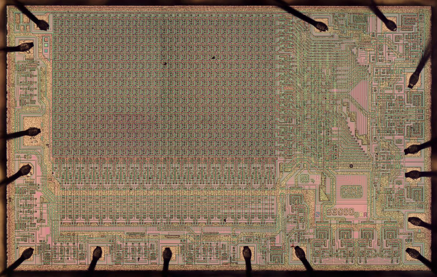
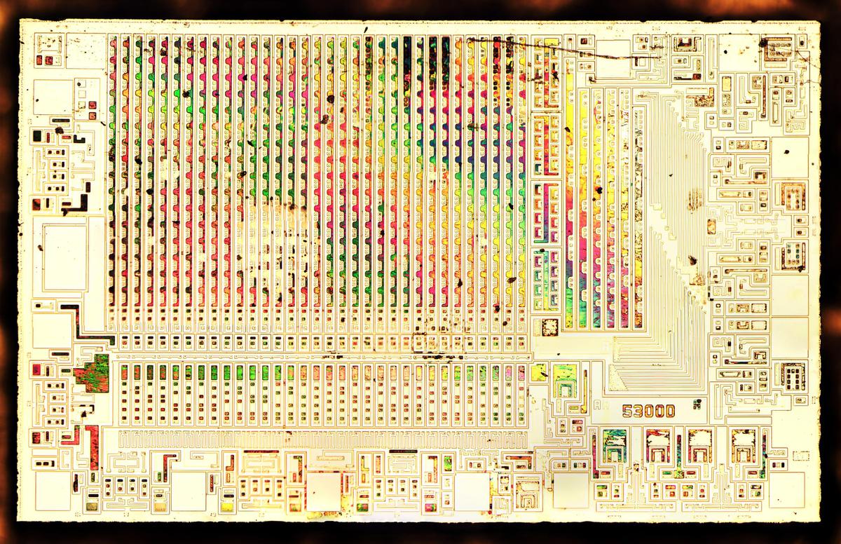
The highly magnified photo below shows the chip's silicon die. The metal layer on top of the silicon is most visible in this photo; the transistors and resistors fabricated from silicon are underneath. The wires around the edges are the 16 bond wires between the silicon die and the external pins. In the upper left, the 1024 bits of data are stored in a 33×33 array of diodes and fuses. (I'll explain the extra row and column below.) This chip is built from NPN transistors, unlike the MOS transistors used in most modern chips.
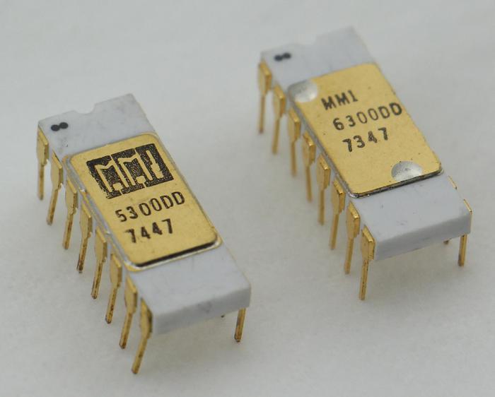
To produce the die photo, I started with the chips below, in their 16-pin ceramic packages; the 5300 and 6300 chips are essentially the same.2 Since the chips were in ceramic packages, I could decap the chip simply by knocking the metal lid off with a chisel, revealing the silicon die.
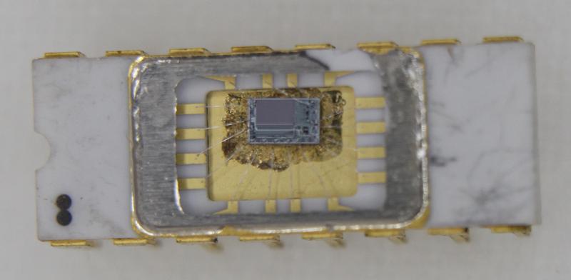
In the photo below, the silicon die is mounted very off-center in the package. It's unclear if that is intentional or sloppy manufacturing. Tiny bond wires connect the die to the metal contacts of the package.
Inside the chip
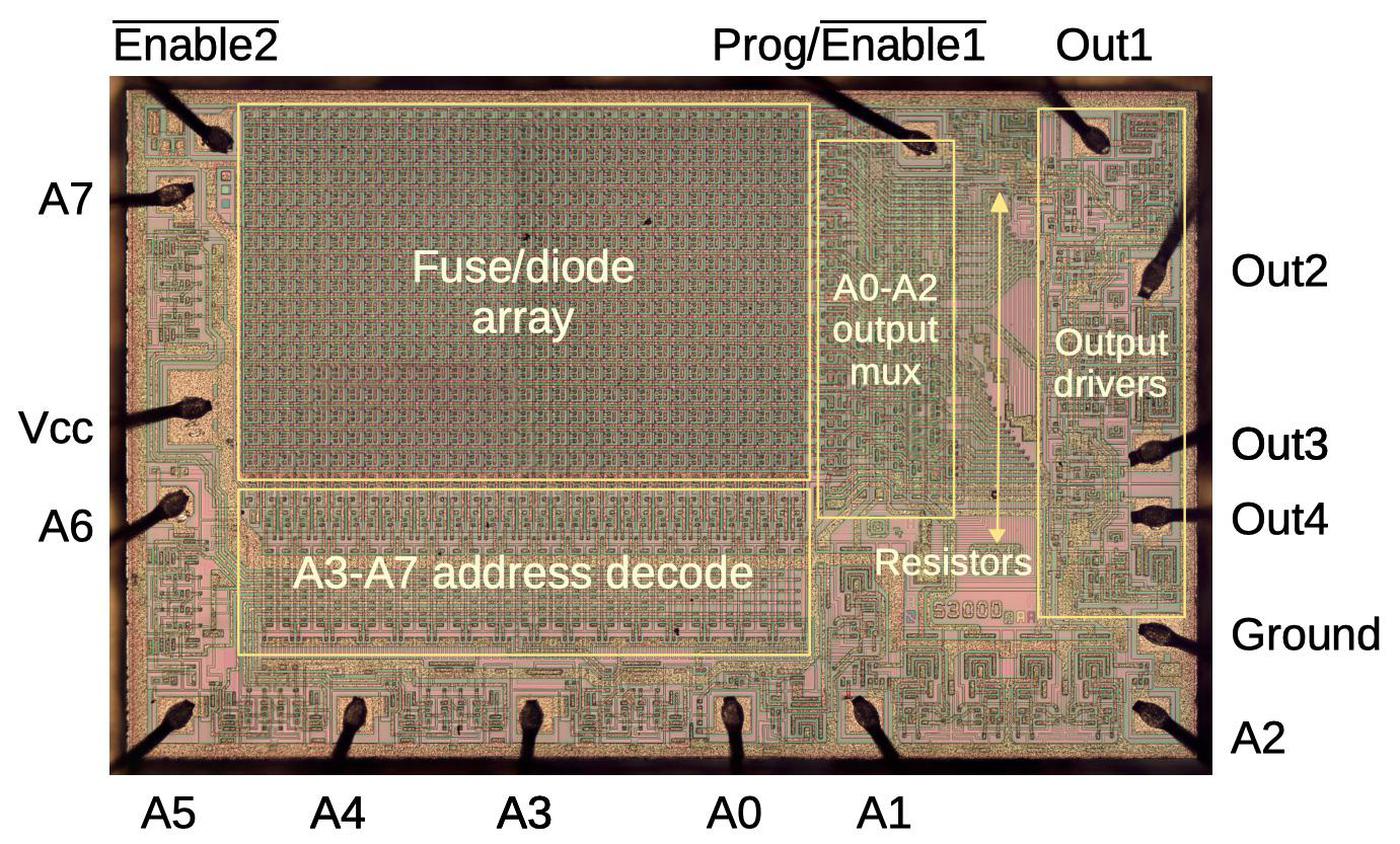
The diagram below shows the main parts of the chip, with the pins labeled. The chip stores 1024 bits as 256 4-bit words. The 8 address lines A0-A7 select one of the 256 words, and the bits are output on pins Out1-Out4. The Program pin is used to store data in the chip by blowing fuses. The Vcc and ground pins power the chip.
The 1024 bits of data are stored in a 33×33 array of diodes and fuses. Note that the data array only takes up about a quarter of the chip; the rest of the chip holds the supporting circuitry. Below the data array, address decode circuitry used the address lines to select one of 32 columns in the array. To the right, DTL multiplexers4 reduced the 32 rows of output to the 4 desired outputs. The output drivers amplified these signals and sent them to the output pins.
The fuses
The chip stored data in tiny fuses. An intact fuse represented a 1, while a blown fuse represented a 0. Thus, the chip was shipped containing all 1's, and the user programmed the chip by blowing fuses where a 0 bit was required. The fuses were fabricated from tiny regions of Nichrome metal that heat up and melt under high voltage. (Nichrome is a nickel-chromium alloy that has much higher resistance than typical metals, causing it to heat up. It is commonly used in applications such as toasters.)
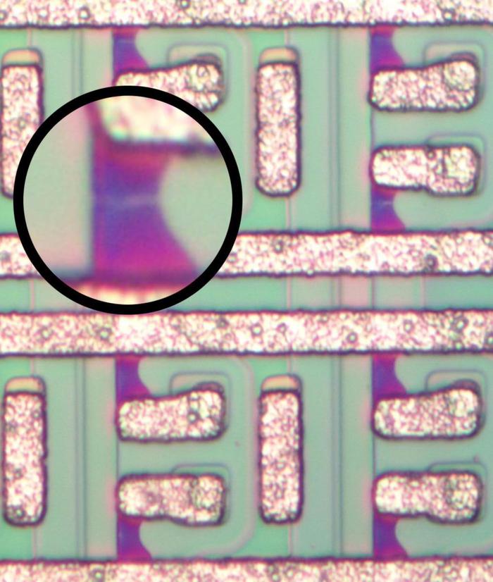
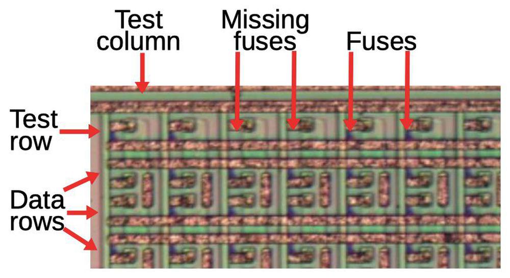
The fuses are visible in the die photo above; they are the purple regions between the metal wiring. The fuses are very small, about 8µm long. I expected a blown fuse would vaporize entirely, but instead a blown fuse contains a tiny crack roughly 700 nm wide. (This is the wavelength of red light, so the crack is just barely visible under the microscope.)
Address decoding
The PROM stored 1024 bits as 256 words of 4 bits. However, the bits are physically arranged in a 33×33 grid since a square memory grid is more efficient than a highly-rectangular one. To access the memory, address bits A3-A7 select one of the 32 columns. The selected 32 bits in the column go through the multiplexers at the right, which select one bit out of each group of eight, based on address bits A0-A2. The four selected bits become the four outputs. Thus, addressing has two parts—one to select the column and one to select the four output bits—and they have separate circuitry,
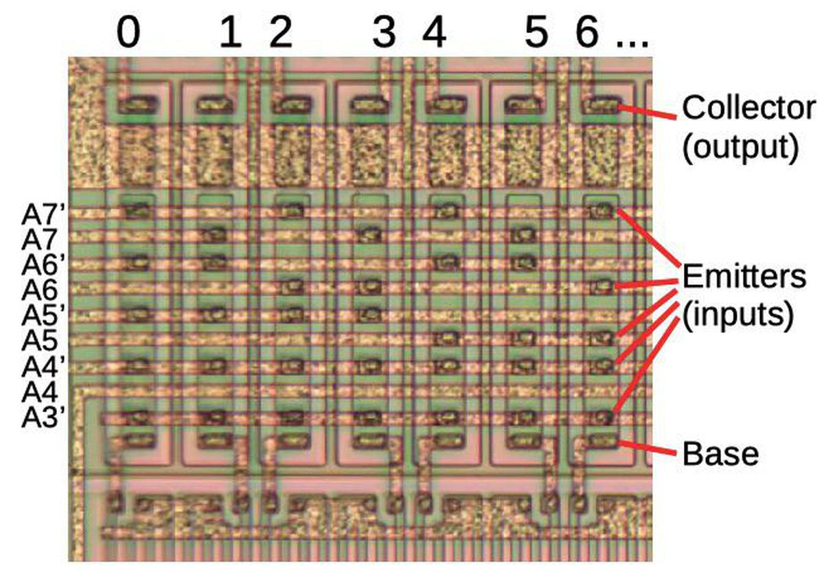
Column selection uses 32 NAND gates, implemented with multiple-emitter transistors.3 (The N and P silicon regions of the transistors are visible as rectangular boxes, with the brownish metal layer on top connecting the regions together.) Each NAND gate has a different combination of address bits A3-A7 either inverted or uninverted, so each address activates a different NAND gate, selecting the associated column. You can see the binary counting in the emitters. The A7' and A7 lines alternate connections every column. The A6'/A6 connections alternate every two columns, while A5'/A5 alternate every four, and so on.
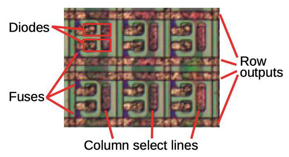
The data array consists of a diode and fuse for each bit. (Without diodes, the bits would all be shorted together.) If the fuse is present, a low signal on the selected column will pull the corresponding row low through the diode (indicating a 1). If the fuse is blown, the row will remain high (indicating a 0). Thus, by blowing fuses, bits are programmed into the memory array. The diodes themselves are mostly hidden under the metal layer below. The column select lines run vertically in the silicon under the metal layer; the metal stripes on top reduce the resistance.
Programming
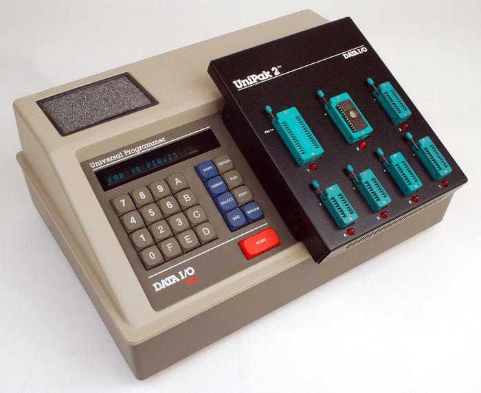
To program the PROM, the user melted the necessary fuses one at a time using carefully-controlled high voltage pulses. After selecting the desired address, 27 volts was applied to the programming pin (a much higher voltage than the typical 5V TTL level). After a carefully-timed interval, the desired output was brought to 20 volts for a few microseconds to blow the fuse. (The timing and voltages needed to be precise so the fuse would blow without damaging other parts of the chip.) The process was repeated for each desired 0 bit. Customers used a PROM programmer such as shown below to perform these operations automatically.
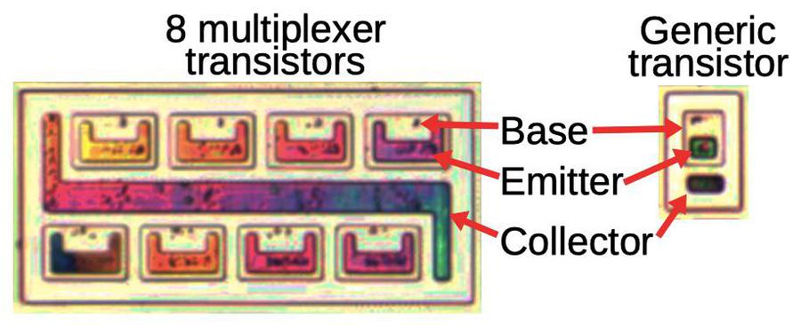
For the most part, reading a fuse and blowing a fuse used the same circuitry; the difference was the output pin circuit, which could either output a bit or sink a large current to blow the fuse, depending on the programming mode.5 The transistors along the programming path were larger than regular transistors to handle the larger current. For example, the diagram below compares the multiplexer NPN transistors to a typical NPN transistor on the chip. Also note that the 8 transistors in a multiplexer share a single collector (the multiplexer output).
Testing
Before examining this chip, I didn't consider how difficult it was for the manufacturer to test a PROM. Most chips can be extensively tested before shipping to the customer, but you can't test the PROM fuses without irreversibly programming the chip. Even testing the address decode logic is difficult; since the chip is manufactured with all 1's, you'd read the same result even if the address circuitry is broken.
To support testing, the chip contains an extra row and column of fuses.6 As a result, the storage grid was 33×33, rather than the 32×32 grid you'd expect. Half of the test fuses were missing, so reading the correct pattern of 0's and 1's tested the address decoders. By blowing test fuses and reading the results, the programming characteristics could be tested. The datasheet says that the chips should have a programming yield of over 95%. Compared to most integrated circuits, this is a high failure rate, but it's understandable given the difficulties of testing the chip.
Unused circuitry
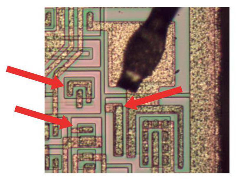
One interesting feature of the 5300 die is that it has some transistors that aren't connected to anything else in the chip. The diagram below shows some of the unused transistors in the output circuitry. There are no metal connections from these transistors to the rest of the chip, making them apparently useless.
The reason for these unused transistors is that the same silicon layout could be used for slightly different PROM chips, depending on how the metal layer was wired up. The 5300 PROM had open-collector outputs, but a tri-state version (6301) was also available.7 Both chips used the same silicon die, but had small modifications to the metal layer to wire the transistors differently. Since the 5300 didn't need output transistors to pull the output to 1, these were left unconnected, yielding the unused circuitry seen above.
Conclusion
PROM chips were an important part of early computer systems, often holding the boot code, but their popularity peaked in the early 1980s as they were replaced by erasable PROM (EPROM) chips. EPROM chips had a distinctive quartz window over the die; shining ultraviolet light on the chip erased it, so it could be reused. EPROMs in turn were replaced by electrically-erasable PROMs (EEPROMs), similar to flash memory. To see how much technology has improved, consider that the 6300 PROM chip cost $70 in 1971 and stored 128 bytes. Now you can get a 128 GB flash drive for under $20: a billion times the storage, plus you can write it more than once.
I announce my latest blog posts on Twitter, so follow me @kenshirriff for future articles. I also have an RSS feed. Thanks to Marc Verdiell for supplying the chip.
Notes and references
-
For more information on the chip, see the MMI Bipolar LSI Databook chapter 2. ↩
-
The 6300 was the commercial 1K PROM, while the 5300 was the same chip specified for the military temperature range (-55 °C to +125 °C). The 6200/5200 was a compatible ROM chip, so you could design your system using the 6300 PROM and then drop in a mask-programmed ROM when everything was working. (A mask-programmed ROM was cheaper, but needed to be manufactured in large quantities.) ↩
-
Multiple-emitter transistors may seem strange, but they are used in the common 7400-series TTL chips. ↩
-
I suspect that diode-transistor logic was used instead of TTL for the output multiplexer because the simpler DTL circuit worked better with the high programming voltages. The DTL circuitry uses very large resistors biased to the programming voltage. They are visible near the right side of the die. ↩
-
The current path for reading and programming bits is as follows. When reading a bit, the output driver circuit was pulled to ground through a multiplexer transistor, the (intact) fuse, the associated diode, and finally the column select transistor. To blow a fuse, the programming pulse disabled the output driver circuits and transistors connected the output pins directly to the multiplexers. Then the high voltage pulse on the output pin followed the same path as before (multiplexer transistor, fuse, diode, column select transistor and ground), but the much higher current blew the fuse, permanently switching the bit to 0. ↩
-
One interesting question is how the test fuses are accessed. There are no test points on the chip; from the circuitry it appears that these fuses are accessed by applying unusual voltages to some of the pins. To access the row of test fuses at the top of the chip, the programming pin is raised to a higher voltage. To read or write the column of test fuses at the left of the chip, address pin A6 is pulled higher. This allows the row select logic, output drivers and programming circuitry to be tested. (These actions are undocumented and based on my reverse engineering.) ↩
-
The motivation for using tri-state or open-collector outputs is that often multiple memory chips were connected together to create a larger memory. The problem was how to combine the outputs. One solution was "open collector" outputs: essentially an output is either 0 or "nothing", and an external resistor pulls the output to 1 if it's not 0. A second solution was tri-state outputs: an output can be 0, 1, or "nothing" if not enabled. Since only one output was enabled at a time, the outputs could be tied together. ↩
ReplyDeleteI thought I had seen it all.
Now I see that no.
I had not imagined a technique of blowing micro fuses to create a ROM.
A very efficient context for the time.
Thanks again for the excellent article.
Fuse technology at MMI and later at AMD (which acquired MMI) used several different materials. AMD/MMI PALs used Platinum Silicide (PlSi) and Titanium Tungsten (TiW). I remember seeing photo micrographs of Nichrome fuses that looked like two interdigitated combs, with a lot of debris in the blown fuse area. The Nichrome fuses had a reputation for being unreliable, and "growing back". The PlSi and TiW fuses were more reliable. Their photo micrographs looked like the material melted and then while liquid, surface tension made the material roll back to the unmelted material, leaving a much cleaner area in blown fuses.
ReplyDeleteThank you very much for an informative and entertaining article! Did you mean "the tiny horizontal crack" instead of "the tiny vertical crack" in the description of the photo with the fuses? Can't quite see how a vertical crack would constitute a blown fuse.
ReplyDeletesomehow I was expecting a "blown" bit to be much more obvious, its amazing what you're able to see, "near the wavelength of red light"... amazing, keep up the great work!
ReplyDeleteAn alternative to fuses were "anti-fuses" made from essentially base-emitter junctions. But when a high current is applied, they go from open to short. "Zener zapping" used to trim analog parts is the same thing.
ReplyDeleteWhat geometry did this chip use?
ReplyDeleteGreat teardown!
spb_nick: you are correct. I rotated the image and forgot to update the text.
ReplyDeleteThis is an extremely informative article. As the MMI salesman in the 1970s who received these chips as samples and held on to them for eons, I was not aware of the geometries, testing difficulties, or yield estimates. I am so glad that Marc was able to get them into the hands of such an expert who articulated the complexities of bipolar PROM manufacturing in that era. There is an application note I retained that mentions how useful these smaller chips are for patches in firmware. It should be noted that the APPLE I used the tristate version of these chips and they are mentioned on the schematic as vendor but incorrectly using the O.C. part number if I'm remembering correctly.
ReplyDeletehttp://cini.classiccmp.org//aim65/MMI-535.pdf
DeleteAmazing how small the blown fuses are, no wonder they had reliability problems! Could you elaborate on footnote #6? It seems strange that the programming solution was so complicated when test points could've easily been added and probed during the check process.
ReplyDeleteIt's also fairly apparent why MOS technology took over. One of the chips I simulated fit a ROM with 16x the capacity, the necessary decoding circuitry, a simple serial bus, a microcontroller, a digital filter, and a PWM engine all onto a single chip! And that was possible in 1980!
Similar devices were the mainstay of the electronic security industry, used to store telephone and account numbers in automatic alarm diallers. 74S287 comes to mind, and they were used in thousands on both sides of the Atlantic.
ReplyDeleteHere is a boock about the history of analog computing.
ReplyDeletehttps://books.google.de/books?id=y1DpBQAAQBAJ&lpg=PA38&dq=Hoelzer+1941&pg=PA38&redir_esc=y#v=onepage&q=Hoelzer%201941&f=false
Hello:
ReplyDeleteMy name is Paul R. Ward, and I was a Mictolithography Process Engineer at the MMI Sunnyvale Facility from 1980 to 1985 - I worked on these parts, which were part of a series of varying sized Fuse Proms, such as the 5300, 5340, 5350, 5370, and 5390. All used Negative Photoresist technology, 5 micron lines and spaces, and were imaged on Perkin Elmer Micralign 140s. The Metalization, when I started, was done with Evaporators, but we moved to Sputtering systems as time went by, also transitioning from wet processing to Plasma Etching for certain processes.
The NiCr fuses, when I started, were done with Negative photoresist as a lift off ( scrub off ) process. You imaged the layer of photoresist with tiny bow-tie shaped windows, evaportated the NiCr metal, and then removed the photoresist with an organic stripper, after which the excess NiCr. was scrubbed off the waters using alcohol soaked Q tips on a cobilt wafer spinner. In early 1981, we converted the process to Positive photoresist, using the same masks, which meant that the metal was deposited first, then masked with the Fuse Mask, after which the unwanted metal was etched off with a dilute solution of Nitric Acid and a trace of Ceric Ammonium Nitrate. A much better process, with a much higher yield.
A major problem that was only solved when we went to sputtering systems ( P.E. 2400s and 4410s ) was the Ni to Cr ratio, which dramatically affected the Fuse Blowing Current and Temperature. Once we went to Sputtering the metal, those problems went away. Just in
time for the parts to become obsolete......
In Fab IV in Sunnyvalewe we also made some of the first Fuse PALs, using Titanium Tungsten ( TiW) fuses, which had their own problems, as they had to be etched with Hydrogen Peroxide, a tricky and troublesome process to manage.
Forty Years ago. I was about to say that it seems like a lifetime has passed, but, in fact, it has. I was a 25 year old budding Process Engineer in the summer of 1980. Now I've retired. But Silicon Valley was the place to be in the 1970s-1980s !
Paul R. Ward
Thanks Paul for the technical aspects of the wafer fab
DeleteI started as a green EE in 1978 at a company called Ramtek, also of Sunnyvale. We used the 5300 PROM's among others, blowing them on a DataIO programmer. Shortly prior to my arrival they had started using MMI PAL's, one of the first companies to do so if not the first. This was before some marketing guy at MMI wrote PALSAM, so the RAMTEK engineers had to figure out all the 1's and 0's by hand. Ramtek was a spinoff of Data Disk, which had built bitmapped graphics displays using synchronized disk drives. Ramtek instead started out using Intel 1101 256bit static RAM's in the early 70's, buying parts cheaply that didn't meet spec (before my time, I could have that wrong). My first project was working on their low end product, a rack mount system that used 4kbit 4027 DRAM's to display 320x240 pixels in color on a 15khz CRT for maybe $5k. But the Apple II was out, the cheap CGA cards for the IBM PC were on the way, and the Ramtek 6110 was a very hard sell.
ReplyDeleteWhat would prevent an already fielded chip from being reprogrammed by blowing additional fuses? Or were these only used for prototyping? I think i read somewhere that some secure crypto modules used them to store keys, which means that being able to force additional bits to zero might have security implications.
ReplyDeleteBecause of their cost, previously blown devices were recycled by overlayin the new pattern to see if additional fuses could be blown to fit the new pattern.
DeleteFor crypto modules, blowing additional fuses can be done to erase the key. So, indeed, a very positive security implication. Corrupting the key is enough to make the module unusable, but the key is recoverable if only a few bits were affected. Once the majority of the key is "blown", i.e. overwritten, the key material is forever secure from recovery.
ReplyDeleteI've found a cache of new old stock MMI PALs in Norway of all places, and they are delightful devices to use. Excellent for TTL homebrew computer projects - they save on discrete chips. In fact, that case of chips was so big that thousands of them were tossed away already, but still quite a few remain :)
Another MMI tidbit: the MMI PALs are programmed essentially the same as the MMI PROMs from the same era. Just the pinout is different. MMI was kind enough to publicly document the programming method for their fuse-based PROMs and PALs. I wish other companies did so - every one of them becomes defunct eventually, or their product becomes defunct, and the documentation is only preserved in the programming tool vendor R&D lab somewhere. Then the programming tool vendor becomes defunct, and the paper documentation and its facsimiles are gone. Then it takes to run an old programmer on some devices, with data capture set up to record the whole process to reverse-engineer it :(
ReplyDeleteI thought I'd publish the link to MMI programmer. It's in my pages on Rich Cini classic
ReplyDeletehttp://cini.classiccmp.org//aim65/MMI-535.pdf
I can only speculate that the chip offset is intended to minimize the high current circuits
ReplyDelete