Have you ever wondered what's inside your computer's power supply? The task of a PC power supply is to convert the power from the wall (120 or 240 volts AC) into stable power at the DC voltages that the computer requires. The power supply must be compact and low-cost while transforming the power efficiently and safely. To achieve these goals, power supplies use a variety of techniques and are more complex inside than you might expect. In this blog post, I tear down a PC power supply and explain how it works.1
The power supply I examined, like most modern power supplies uses a design known as a "switching power supply." Switching power supplies are now very cheap, but this wasn't always the case. In the 1950s, switching power supplies were complex and expensive, used in aerospace and satellite applications that needed small, lightweight power supplies. By the early 1970s, though, new high-voltage transistors and other technology improvements made switching power supplies much cheaper and they became widely used in computers. Now, you can buy a phone charger for a few dollars that contains a switching power supply.
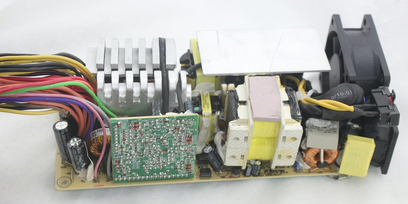
The ATX power supply that I examined was packaged in a metal box the size of a brick, with a remarkable number of colorful cables emerging from it. Removing the case reveals the components below, tightly packed to keep the power supply compact. Many of the components are hidden by the heat sinks that keep the power semiconductors cool along with the fan at the right.
I'll start with a quick overview of how the switching power supply works, and then describe the components in detail. Starting at the right, the power supply receives AC power. The input AC is converted to high-voltage DC, with the help of some large filtering components. This DC is switched on and off thousands of times a second to produce pulses that are fed into a transformer, which converts the high-voltage pulses into low-voltage, high-current pulses. These pulses are converted to DC and filtered to provide nice, clean power, which is fed to the computer's motherboard and disk drives through the bundle of wires on the left.
While this process may seem excessively complex, most consumer electronics, from your cell phone to your television, use a switching power supply. The high frequencies allow the use of a small, lightweight transformer. In addition, switching power supplies are very efficient; the pulses are adjusted to supply just the power needed, rather than turning excess power into waste heat as in a "linear" power supply.
Input filtering
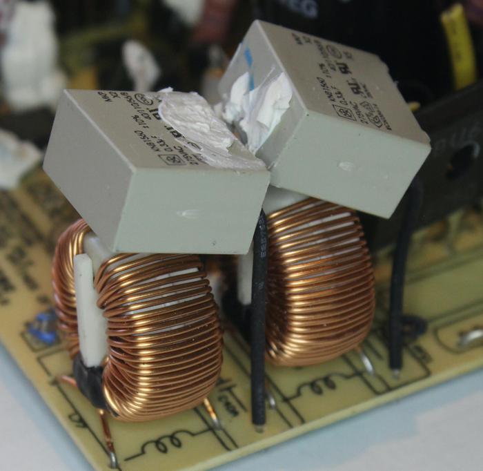
The first step is for the input AC to go through an input filter circuit that blocks electrical noise from exiting the power supply. The filter below consists of inductors (the toroidal coils) and capacitors. These boxy gray capacitors are special Class-X capacitors, designed to be connected safely across the AC lines.
Rectification: converting AC to DC
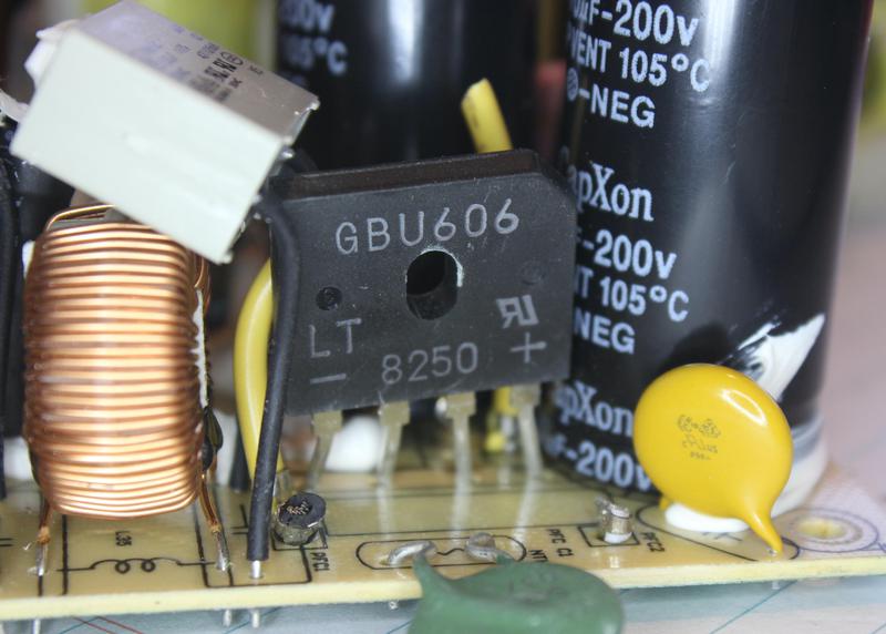
The 60-Hertz AC (alternating current) from the wall oscillates 60 times a second, but the power supply needs steady DC (direct current) that flows in one direction. The full-bridge rectifier below converts the AC to DC. The rectifier below is marked with "-" and "+" for the DC outputs, while the two center pins are the AC input. Internally the rectifier contains four diodes. A diode allows current to pass in one direction and blocks it in the other direction, so the result is that the alternating current is converted to direct current, flowing in the desired direction.
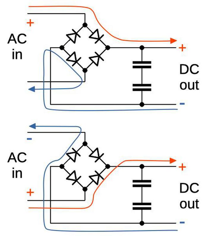
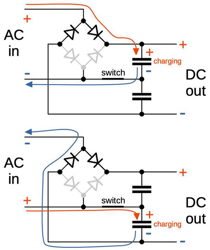
The diagram below shows how the bridge rectifier works. In the first schematic, the AC input has the upper side positive. The diodes pass the voltage through to the DC output. In the second schematic, the AC input has reversed direction. However, the configuration of the diodes ensures that the DC output voltage stays the same (positive on top). The capacitors smooth out the output.
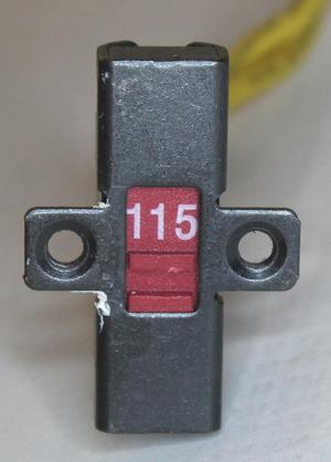
Modern power supplies accept a "universal" input voltage of 85 to 264 volts AC, so they are usable in different countries regardless of the country's voltage. However, the circuitry of this older power supply couldn't handle such a wide input range. Instead, you had to flip a switch (below) to select between 115 V and 230 V.
The voltage selection switch used a clever circuit, a voltage doubler. The idea is that with the switch closed (for 115 volts), the AC input bypasses the bottom two diodes in the bridge rectifier and is instead connected directly to the two capacitors. When the AC input is positive on top, the top capacitor is charged with the full voltage. And when the AC input is positive on the bottom, the lower capacitor is charged with the full voltage. Since the DC output is across both capacitors, the DC output has double the voltage. The point of this is that the rest of the power supply receives the same voltage, whether the input is 115 volts or 230 volts, simplifying its design. The downsides of the voltage doubler are that the user must put the switch in the correct position (or risk destroying the power supply), and the power supply requires two large capacitors. For these reasons, the voltage doubler has gone out of style in more recent power supplies.
Primary and secondary
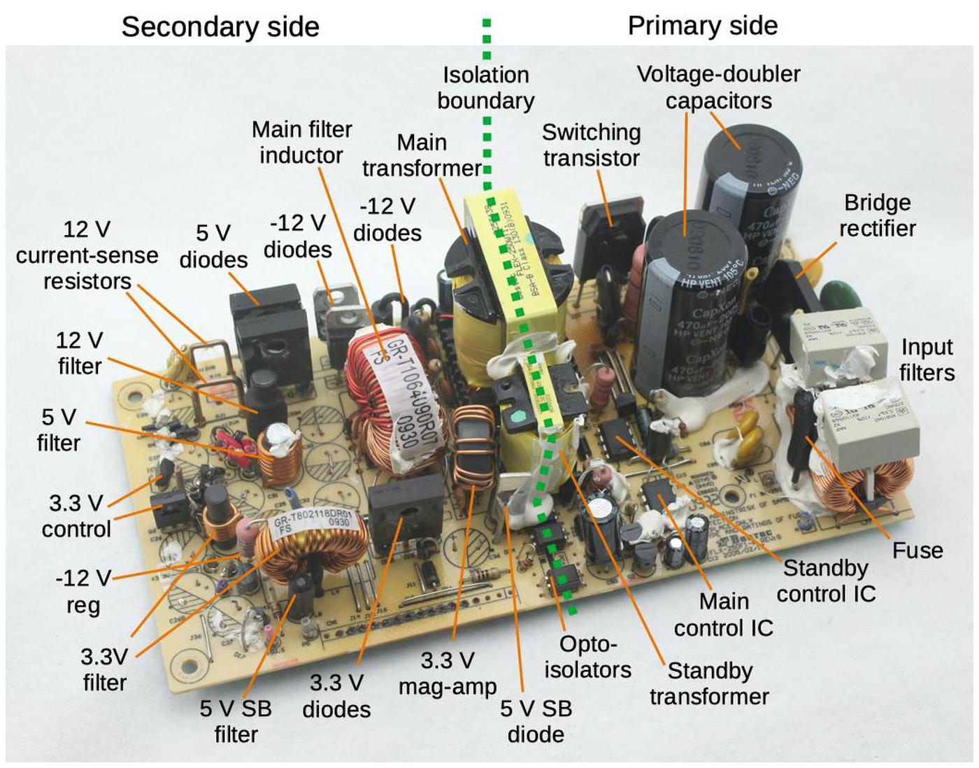
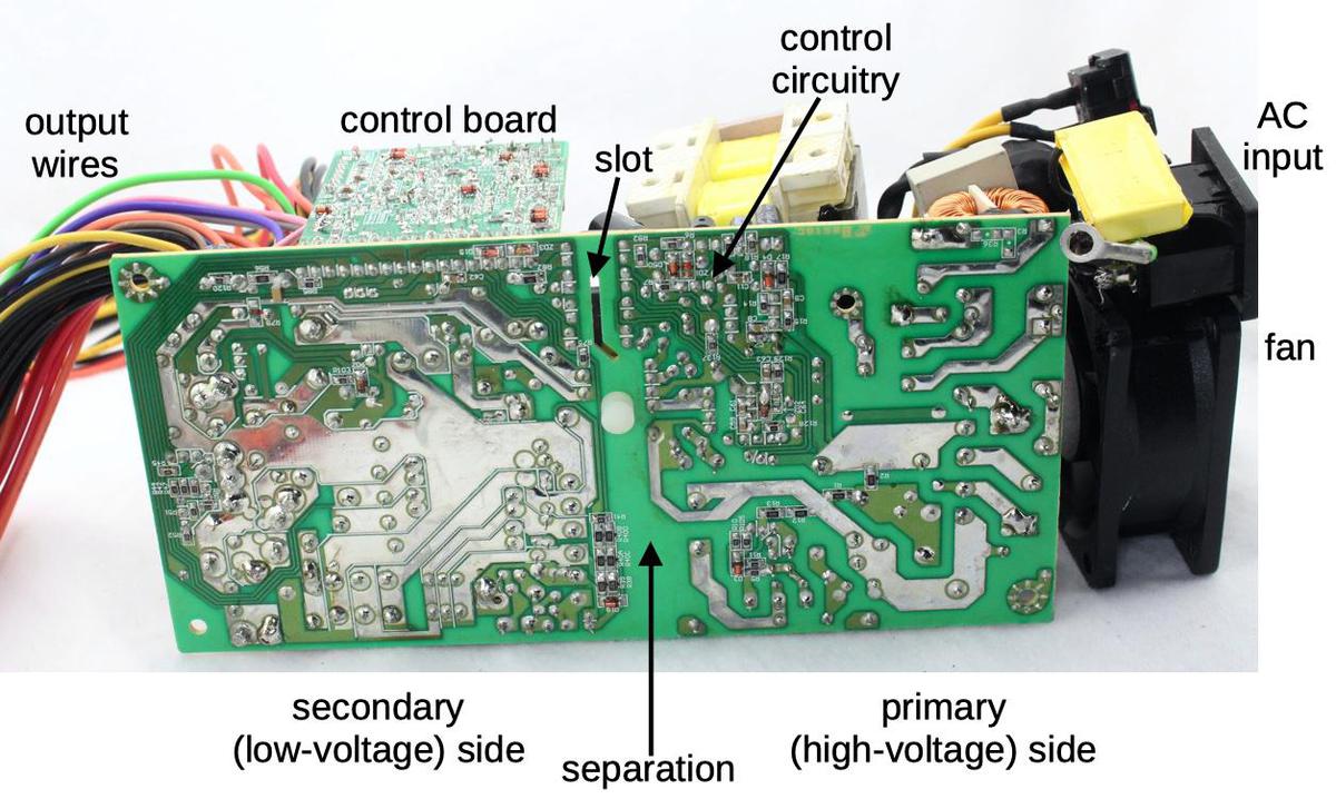
For safety, the high-voltage components and the low-voltage components are separated, both mechanically and electrically. The primary side below contains all the circuitry that is connected to the AC line. The secondary side contains the low-voltage circuitry. The primary and secondary are separated by an "isolation boundary" (shown in green), with no electrical connections across the boundary. The transformers pass power across this boundary through magnetic fields, without a direct electrical connection. Feedback signals are sent from the secondary to the primary by opto-isolators, which transmit signals optically. This separation is a key factor in safe power supply design: a direct electrical connection between the AC line and the output would create a high danger of electric shock.
Pulses to the transformer
At this point, the input AC has been converted to high-voltage DC, about 320 volts.2 The DC is chopped into pulses by the switching transistor above, a power MOSFET.3 Because this transistor gets hot during use, it was mounted on a large heat sink. These pulses are fed into the main transformer above, which in a sense is the heart of the power supply.
The transformer consists of multiple coils of wire wound around a magnetizable core. The high-voltage pulses into the transformer's primary winding produce a magnetic field. The core directs this magnetic field to the other, secondary windings, producing voltages in these windings. This is how the power supply safely produces its output voltages: there is no electrical connection between the two sides of the transformer, just a connection by the magnetic field. The other important aspect of the transformer is that the primary winding has the wire wrapped around the core a large number of times, while the secondary windings are wrapped around a much smaller number of times. The result is a step-down transformer: the output voltage is much smaller than the input, but at a much higher current.
The switching transistor3 is controlled by an integrated circuit, a "UC3842B current mode PWM controller". This chip can be considered the brains of the power supply. It generates pulses at the high frequency of 250 kilohertz. The width of each pulse is adjusted to provide the necessary output voltage: if the voltage starts to drop, the chip produces wider pulses to pass more power through the transformer.4
The secondary side
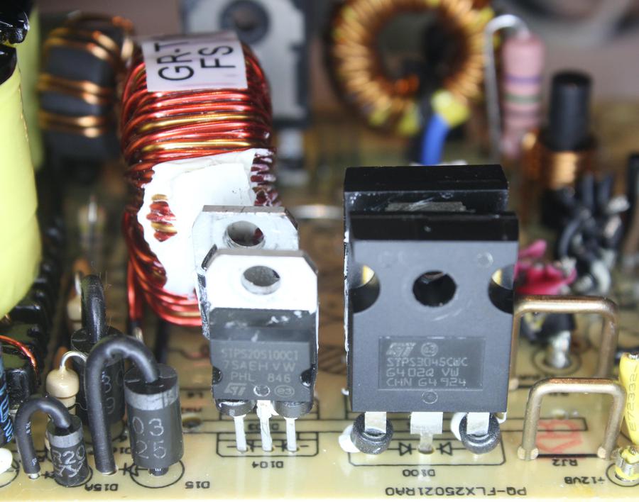
Now we can look at the secondary side of the power supply, which receives the low-voltage outputs from the transformer. The secondary circuitry produces the four output voltages: 5 volts, 12 volts, -12 volts, and 3.3 volts. Each output voltage has a separate transformer winding and a separate circuit to produce that voltage. Power diodes (below) convert the outputs from the transformer to DC, and then inductors and capacitors filter the output to keep it smooth. The power supply must regulate the output voltages to keep them at the proper level even as the load increases or decreases. Interestingly, the power supply uses several different regulation techniques.
The main outputs are the 5-volt and 12-volt outputs. These are regulated together by the controller chip on the primary side. If the voltage is too low, the controller chip increases the width of the pulses, passing more power through the transformer and causing the voltage on the secondary side to increase. And if the voltage is too high, the chip decreases the pulse width. (The same feedback circuit controls both the 5-volt and 12-volt output, so the load on one output can affect the voltage on the other. Better power supplies regulate the two outputs separately.5)
You might wonder how the controller chip on the primary side receives feedback about the voltage levels on the secondary side, since there is no electrical connection between the two sides. (In the photo above, you can see the wide gap separating the two sides.) The trick is a clever chip called the opto-isolator. Internally, one side of the chip contains an infra-red LED. The other side of the chip contains a light-sensitive photo-transistor. The feedback signal on the secondary side is sent into the LED, and the signal is detected by the photo-transistor on the primary side. Thus, the opto-isolator provides a bridge between the secondary side and the primary side, communicating by light instead of electricity.6
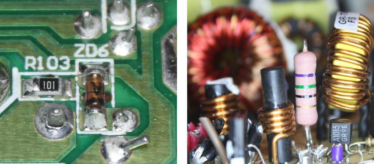
The power supply also provides a negative voltage output (-12 V). This voltage is mostly obsolete, but was used to power serial ports and PCI slots. Regulation of the -12 V supply is completely different from the 5-volt and 12-volt regulation. The -12V output is controlled by a Zener diode, a special type of diode that blocks reverse voltage until a particular voltage is reached, and then starts conducting. The excess voltage is dissipated as heat through a power resistor (pink), controlled by a transistor and the Zener diode. (Since this approach wastes energy, modern high-efficiency power supplies don't use this regulation technique.)
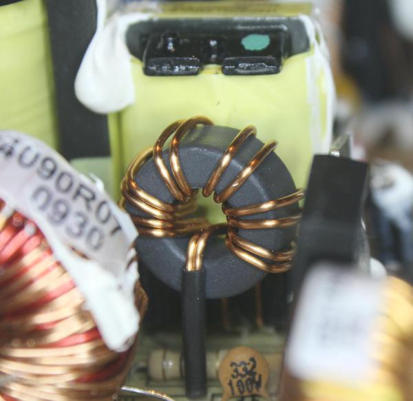
Perhaps the most interesting regulation circuit is for the 3.3-volt output, which is regulated by a magnetic amplifier. A magnetic amplifier is an inductor with special magnetic properties that make it behave like a switch. When a current is fed into the magnetic amplifier inductor, at first the inductor will almost completely block the current as the inductor magnetizes and the magnetic field increases. When the inductor reaches its full magnetization (i.e. it saturates), the behavior suddenly changes and the inductor lets the current flow unimpeded. In the power supply, the magnetic amplifier receives pulses from the transformer. The inductor blocks a variable part of the pulse; by changing the pulse width, the 3.3-volt output is regulated.7
The control board
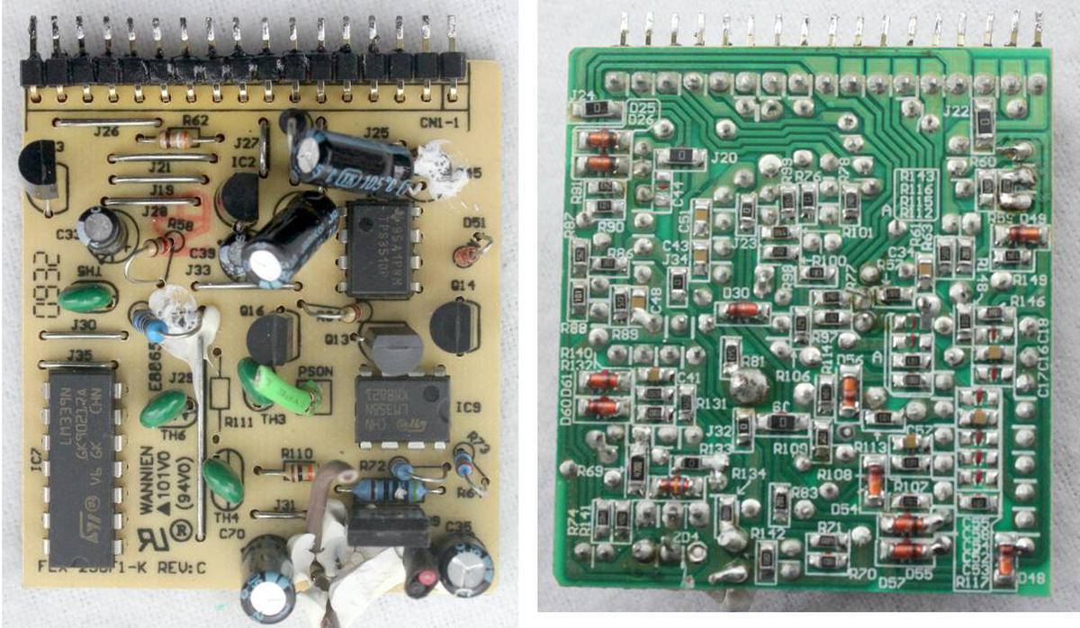
The power supply has a small board holding the control circuitry. This board compares the voltages against a reference to generate the feedback signals. It also monitors the voltages to generate a "power good" signal.8 This circuitry is mounted on a separate, perpendicular board so it doesn't take up much room in the power supply.
The standby power supply
The power supply contains a second circuit for standby power.9 Even when the computer is supposedly turned off, the 5V standby supply is providing 10 watts. This power is used for features that need to be powered when the computer is "off", such as the real-time clock, the power button, and powering-on via the network ("Wake on LAN"). The standby power circuit is almost a second independent power supply: it uses a separate control IC, separate transformer, and components on the secondary side, although it uses the same AC-to-DC circuitry on the primary side. The standby power circuit provides much less power than the main circuit, so it can use a smaller transformer.
Conclusion
An ATX power supply is complex internally, with a multitude of components ranging from chunky inductors and capacitors to tiny surface-mount devices.10 This complexity, however, results in power supplies that are efficient, lightweight, and safe. In comparison, I wrote about a power supply from the 1940s that produced just 85 Watts DC, but was suitcase-sized and weighed over 100 pounds. Now, with advanced semiconductors, you can hold a much more powerful power supply for under $50 that you can hold in your hand.
I've written about power supplies before, including a history of power supplies in IEEE Spectrum. You might also like my Macbook charger teardown and iPhone charger teardown. I announce my latest blog posts on Twitter, so follow me at kenshirriff. I also have an RSS feed.
Notes and references
-
Intel introduced the ATX standard for personal computers in 1995. The ATX standard (with some updates) still defines the motherboard, enclosure, and power supply configuration for most PCs. The power supply I examined is from 2005, so newer power supplies are more advanced and more efficient. The basic principles are the same, but there are some changes. For instance, regulation using DC-to-DC converters has mostly replaced the magnetic amplifier.
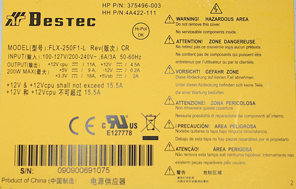
The label on the power supply.The label provides information about the power supply I examined. It was built by Bestec for Hewlett-Packard's Dx5150 desktop PC. This power supply doesn't fit the ATX dimensions; it is longer and more rectangular. ↩
-
You might wonder why an AC input of 230 volts yields 320 volts DC. The reason is that AC voltage is normally measured as root-mean-square which (sort of) averages the varying waveform. As a result, a 230-volt AC signal has peaks of 320 volts. The power supply capacitors charge through the diodes to the peak voltage, so the DC will be approximately 320 volts (although it will sag somewhat through the cycle). ↩
-
The power transistor is an FQA9N90C power MOSFET. It can handle 9 amps and 900 volts. ↩↩
-
The integrated circuit is powered by a separate winding on the transformer that provides 34 volts to run the chip. You might notice a chicken-and-egg problem: the control IC creates the pulses to the transformer, but the transformer powers the control IC. The solution is a startup circuit consisting of a 100 kΩ resistor between the IC and the high-voltage DC. This provides a small current, sufficient to start operation of the IC. Once the IC starts sending pulses to the transformer, it is powered by the transformer. ↩
-
The technique of using one regulation loop for two outputs is called cross-regulation. If the load on one output is much higher than the load on the other, the voltages may diverge from their proper values. For this reason, many power supplies have a minimum load requirement on each output. More advanced power supplies use DC-to-DC converters for all the outputs to make sure they are precise. For more about cross-regulation, see this presentation and this presentation. One technique discussed is DC-stacking the output windings, a technique used in this power supply. Specifically, the 12-volt output is implemented as a 7-volt output "stacked" on top of the 5-volt output, yielding 12-volts. With this configuration, a 10% error (for example) in the 12-volt circuit would be just 0.7 V rather than 1.2 V. ↩
-
The opto-isolators are PC817 components, which provide 5000 volts of isolation between the two sides. Note the slot cut in the circuit board underneath the opto-isolators. This provides additional safety, ensuring that dangerous voltages cannot pass between the two sides of the opto-isolator along the surface of the circuit board, for example if there were contamination or condensation on the board. (Specifically, the slot increases the creepage distance.) ↩
-
The pulse width through the magnetic amplifier is set by a simple control circuit. During the reverse part of each pulse, the inductor is partially demagnetized. A control circuit adjusts the demagnetization voltage. A higher demagnetization voltage produces more demagnetization. This causes the inductor to take longer to re-magnetize and thus it blocks the input pulse for a longer time. With a shorter pulse passing through the circuit, the output voltage is decreased. Conversely, a lower demagnetization voltage produces less demagnetization, so the input pulse is blocked for a shorter time. Thus, the output voltage is regulated by changing the demagnetization voltage. Note that the pulse width into the magnetic amplifier is controlled by the control IC; the magnetic amplifier cuts these pulses shorter as needed to regulate the 3.3 V output. ↩
-
The control board contains multiple ICs including an LM358NA op-amp, a TPS3510P supervisor/reset chip, an LM339N quad differential comparator, and an AZ431 precision reference. The supervisor chip is interesting; it is specifically designed for power supplies and monitors the outputs to make sure they are not too high or too low. The AZ431 is a variant of the TL431 bandgap reference chip, which is very commonly used in power supplies to provide a reference voltage. I've written about the TL431 here. ↩
-
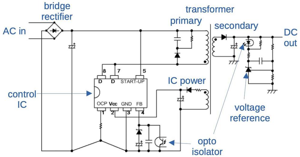
The standby power supply uses a different transformer configuration, called a flyback transformer. The control IC is an A6151, which includes the switching transistor in the IC, simplifying the design.
Power supply circuit using the A6151. This schematic is from the datasheet so it is close to the circuit in the power supply I examined, but not identical. -
If you want to see detailed schematics of a variety of ATX power supplies, see danyk.cz. It's remarkable how many different implementations are used in power supplies: different topologies (half-bridge or forward), absence or presence of power factor conversion (PFC), and different control, regulation, and monitoring systems. The power supply I examined is moderately similar to the forward topology ATX supplies without PFC near the bottom of the page. ↩
Thanks for sharing!
ReplyDeleteThe chip is labelled "GBU606", but the photo caption has a typo that says "GPU606".
ReplyDeleteNice write up!
ReplyDeleteThe mains frequency here is not 60Hz…
ReplyDeleteI first encountered a switching supply when I bought an Apple 2 in 1978.
ReplyDeleteI thoroughly enjoy the fact that you recommended an ElectroBOOM video.
ReplyDeleteAh another fine piece of techno p0rn :p
ReplyDeleteAny chance you could look inside one of the components, like optocoupler, control ic or even mosfet. What makes them so special so that PSU is so efficient compared to the older days. I always thought it’s filled with tiny gnomes, doing electro magic.
Looks like a cold solder joint in the photo at https://static.righto.com/images/atx/zener-w600.jpg.
ReplyDeleteKen, another great write up. However I'm somewhat irritated by the new email format. A) The email is static and doesn't get corrections applied as the website does. B) And this is the killer IMHO, the links in the text are translated into opaque URLs at api.follow.it/trackstatistics/, so I see the anchor text like "wrote about" or "this presentation" but I can't see the target URL. In fact I have to click it to get to it - not all that good from a security perspective. Cheer, Brian.
ReplyDeleteHi Brian, regarding the email subscriptions: The email used to be through Feedburner, but they shut down, so I switched to follow.it. I've passed along your feedback about the tracking links to them, and I'll see if there's a way to use direct links. How did the previous email deail with corrections? I thought it was static too.
ReplyDeleteI studied electrical/electronics at University but I learned more from this post alone! Thanks!
ReplyDeleteHello.
ReplyDeleteFor wanting really detailed explanation on PSUs I can recommend this article on Tom's Hardware: https://www.tomshardware.com/reviews/power-supplies-101,4193.html
Also their reviews of PSUs are excellent (They really dig into various aspects) like this one:
https://www.tomshardware.com/reviews/corsair-ax1500i-titanium-power-supply,4276.html
(I picked this review as PSU has advanced monitoring that can be accessed from application)
"The power supply contains a second circuit for standby power... ... is used for features that need to be powered when the computer is "off", such as the real-time clock, the power button, and powering-on via the network ("Wake on LAN")" and well on x86, keeping the MINIX system running inside the 'Management Engine' which has direct access to the Ethernet hardware.
ReplyDeleteI was not aware of this use of magnetic amplifiers. There is a nice TI paper describing it in detail here: https://www.ti.com/lit/ml/slup129/slup129.pdf
ReplyDeleteIt's an interesting technique and you never know when such things will be useful.
Hi Ken, did you know the new style notification emails via follow.it contain sleazy click-tracking links?
ReplyDeleteProbably the best description of a generic PC Power Supply I have come across.
ReplyDeleteMy green wire broke from the board.Where exactly does it go Many thanks Gary
ReplyDeleteHi, my computer gets on but cannot keep continuing after a few seconds or sometimes a few minutes. So I have changed the power supply and it's now solved. In such a case, which part of my old power supply has failed? I wanna repair that for learning. Please suggest me. Many thanks.
ReplyDeleteSorry for necro. This is a great write-up.
ReplyDeleteIt is worth updating, that many newer ATX power supplies produced nowadays no longer use separate windings for different main output voltages. Instead, they are essentially big 12V supplies with other output voltages (except for standby) generated from 12V using VRM modules. This allows for much better efficiency.
Supplies of this type can easily be recognized by reading the PSUs output power spec: the 12V rail output rating will be close to or equal to the total output power of the entire supply.