When a computer executes a machine language instruction, it breaks down the instruction into smaller steps that are performed in sequence. For instance, a load instruction might first compute a memory address, then fetch a value from that address, and then store that value in a register. This article describes how the ARM1 processor implements instruction sequencing, performing the right steps in order. I also look briefly at the 6502 and Z-80 microprocessors and the different sequencing techniques they use.
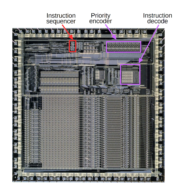
The die photo below shows the ARM1 processor chip, with the relevant functional blocks highlighted. This article focuses on the instruction sequence controller which moves step-by-step through an instruction in sequence. The instruction decode section specifies the steps that need to be performed for each operation and communicates with the sequence controller. The priority encoder tells the sequence controller when to stop block transfer instructions.
You might wonder what relevance a processor from 1985 has today. The ARM1 processor is the ancestor to the immensely popular ARM processor architecture that is used in smartphones and many other systems. Billions of ARM processors have been sold and you probably have one in your pocket now executing the same instructions I discuss in this article. I've written multiple articles about reverse engineering different components of the ARM1; start with my first article for an overview of the chip.
ARM1 instructions and their sequencing
Instructions on the ARM1 range from simple instructions that take one cycle to more complex multi-cycle instructions.[1] Some instructions, such as adding the values in two registers, don't require sequencing because they complete in a single clock cycle. The ARM1 instruction to load a register from memory (LDR) is more complex, consisting of three steps and requiring three clock cycles.[2] In the first step, the memory address is computed. In the second step, the data word is fetched from memory. At the same time, the address register is updated. In the final step, the data is stored into a register. The instruction sequence controller is responsible for stepping through these three steps.
The most complex instructions on the ARM1 are the block data transfer instructions, which read or write multiple registers to memory. A 16-bit bitmask in the instruction specifies the registers to transfer. The number of steps used by the instruction is variable because the read/write step is repeated up to 16 times to copy the specified registers, To support this, the sequence controller implements conditional loops. The ARM1 contains a priority encoder circuit that scans through the register selection bits in order and signals the sequence controller when the transfers are done.
The sequence controller
The instruction sequence controller on the ARM1 is responsible for sequencing the steps of an instruction by providing a cycle number (0 to 3). It also must restart at the end of each instruction. It must repeat cycles as necessary for block transfers.[3]To move between steps, the sequence controller has four sequence operations that it can perform each clock:
END: the instruction ends and an new instruction starts next step.
NEXT: the sequence controller moves to the next cycle number.
IF23: this conditional provides branching and looping for block data transfer —if not done, it stays on cycle 2; otherwise it goes to cycle 3.
IF1E: similar to IF23, if not done, it stays on cycle 1; otherwise it goes to the end cycle (0).
How does the sequence controller know which operation to perform? This information, along with the other control signals, is provided by the instruction decoder. The instruction decoder can be thought of as holding 42 microinstructions, each 36 bits wide.[4] The instruction decoder provides the appropriate microinstruction for each instruction type and cycle number. These microinstruction bits generate control signals for the chip.[5] Two bits in the microinstruction (seqs1 and seqs0) provide the operation to the sequence controller, indicating how to compute the next cycle number. Normally this will be NEXT, until the last microinstruction which specifies END. Thus, the instruction decoder and the sequence controller work together: the sequence controller's cycle number tells the instruction decoder which microinstruction to use, and the instruction decoder tells the sequence controller how to compute the next cycle number.
The sequence controller circuit
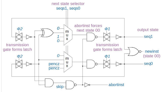
The schematic above shows the circuitry for the instruction sequence controller. The overall idea is the instruction decoder indicates how to compute the next cycle through signals seqs1 and seqs0. The sequence controller produces outputs seq1 and seq0, which tell the instruction decoder the next cycle number. The next cycle values are selected by two multiplexers, which pick one of the four input values based on the control inputs, as shown in the following table. The loop values depend on the pencz signal from the priority encoder, which indicates no more registers to process.
| Input | Seq1 | Seq0 |
|---|---|---|
| 00 (END) | 0 | 0 |
| 01 (NEXT) | seq1' xor seq0' | not seq0' |
| 10 (IF23) | 1 | pencz |
| 11 (IF1E) | 0 | not pencz |
It's straightforward to verify that this logic implements the sequencing described earlier:
Input 00 (END) results in output cycle 0.
Input 01 (NEXT) increments the old cycle (seq1', seq0') by 1.
Input 10 (IF23) will output cycle 2 until pencz is triggered, and then output cycle 3.
Input 11 (IF1E) will output cycle 1 until pencz is triggered and then output cycle 0, the END cycle.
The schematic shows that the sequence controller circuit provides two other outputs. In cycle 0, the circuit outputs the newinst signal, indicating to the rest of the chip that a new instruction is starting. The abortinst signal indicates that the instruction should not be executed because its condition was not satisfied. It is based on the skip input, which comes from the conditional instruction circuit, and is set if the instruction should be skipped.[6] If the instruction should be skipped, abortinst is asserted in cycle 0, forcing the next cycle to be 0 and terminating the instruction after a single cycle. The abortinst signal is also used elsewhere to prevent the skipped instruction from having any effect. Thus, a skipped instruction is effectively a one-cycle NOP instruction.
The implementation of this circuit uses a two-phase clock and dynamic latches to move from step to step. The multi-triangle symbol in the schematic is a transmission gate, used frequently in the ARM1 to build dynamic latches. A transmission gate can be thought of as a switch that closes during the specified clock phase. When the switch opens, the charge stored on the capacitance of the wire holds the previous value, forming a dynamic latch. The clock itself is two phase: First the Φ1 signal is high and the Φ2 is low, and then they alternate. One transmission gate is open during Φ1 and the other is open during Φ2. You can think of it like people moving through double doors: when the first door is open, they can move through it, but must wait for the second door to open. In this manner, the signal progresses through the circuit under the control of the clock and the cycle count updates once per complete clock cycle.
Comparison with the 6502's control logic
This section briefly looks at the 6502 chip, which uses different techniques for sequencing instructions. The 6502 controls each instruction by stepping sequentially through a time step each clock cycle: T0 through T6. Some instructions are quick, ending after two cycles, while others can take all 7 cycles. Instead of a binary counter, the 6502 keeps track of the current T cycle with a shift register with a single active bit that indicates the current cycle (a ring counter). That is, a separate control line is activated during each T cycle, which makes the rest of the control logic easier to implement. When the last T cycle for a particular instruction is reached, the control logic generates a signal (inexplicably called METAL) to reset the shift register to T0 for the next instruction.[7]Interesting 6502 fact: if you execute an illegal instruction known as KIL (kill), the T reset signal doesn't get generated and the timing bit falls off the end of the shift register. The 6502 ends up in no T state at all and stops generating control signals. This locks up the chip until a hardware reset is triggered.
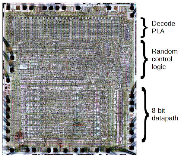
The die photo above shows the layout of the 6502 processor. Note that the control logic (Decode PLA and Random control logic[8] ) takes up about half the chip. At the top, the PLA (Programmable Logic Array) implements the first step of decoding. Below that, the gate logic generates the control signals, using the PLA outputs. The datapath in the bottom part of the chip contains the registers, ALU (arithmetic logic unit), and buses. It performs the operations as instructed by the control signals.
The PLA is a structured collection of NOR gates, which is visible in the die photo as a regular grid. It takes as inputs the instruction and the timing state, and outputs 130 different control signals, which indicate a combination of a timing state and instruction class, such as "T1.DEX" or "T4.X,IND". The PLA outputs are combined and processed by many gates to generate the final control signals, for instance S/SB (connecting the S and SB buses) or SUM (instructing the ALU to compute a sum).
To compare the ARM1 and 6502, they both use sequential timing states to control the instructions but the implementations are different. The 6502 uses a shift register to sequentially move through states. The more complex sequence controller in the ARM1 provides looping on a state. The 6502 has more states (7 vs 4), but looping in the ARM1 allows longer instructions. The ARM1's sequence controller is highly structured, with sequencer "commands" generated by the PLA; an END command reset the sequence controller to end each instruction. The 6502 uses a combination of a PLA and hard-wired logic to control the sequence; the METAL signal resets the shift register to end each instruction.
Comparison with the Z-80's control logic
The Z-80 uses a much more complicated system for instruction sequencing. An instruction is made up of multiple M (memory) cycles, one for each memory access during the instruction. Each M cycle consists of multiple T (time) states. For example an instruction could take 3 T states for the first M cycle and 4 for the second, going through the states: M1T1, M1T2, M1T3, M2T1, M2T2, M2T3, M2T4. More complex instructions can have 6 machine cycles and 23 T states.
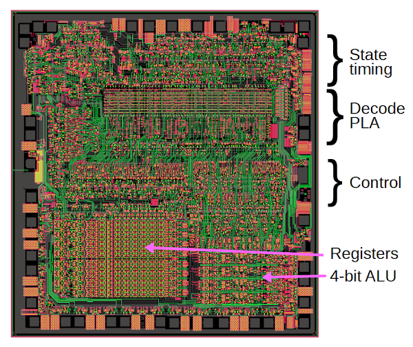
The diagram above shows the layout of the Z-80. The control logic consists of the circuitry to generate the state timing signals, the PLA that decodes instructions,[9] and the random logic to generate control signals below. The chip's datapath (registers and ALU) are at the bottom of the chip. (You may be surprised that the Z-80 has a 4-bit ALU.)
The Z-80's control logic is implemented using a shift register ring counter for the M cycles and a second shift register ring counter for the T states. At the end of an M cycle, the M cycle counter advances to the next cycle and the T state counter resets. Like the 6502, the Z-80 uses a PLA and random logic for instruction decoding, but the details are different. The Z-80 has an AND/OR PLA that generates outputs for different instruction classes, from a single instruction like "LD SP, HL" to larger classes such as a conditional jump or a load. In comparison, the 6502's PLA has a single NOR plane that combines both instruction decoding and timing.
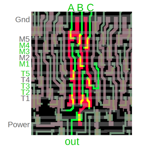
The Z-80 uses complex gates to combine the instruction signals with the timing signals to generate the control signal. A typical gate is structured as: "generate a signal to do something for instruction X in M1T1 or instruction Y in M2T3 or instruction Z in M2T6". The chip layout for these signals has an interesting structure, shown below: the signals T1 to T5 and M1 to M5 run horizontally in the metal layer (faint gray), while the instruction signals (A, B, C) run vertically in polysilicon wires (green). Transistors (yellow) are formed where polysilicon wires cross the silicon (red). This creates a complex, multi-input AND/NOR gate that generates a control signal for the right combination of M, T, and instruction signals. Due to the structure of MOS circuits, this complex gate is constructed as a single gate.
The AND/NOR gate above computes
not ((A and M4 and T3) or (B and M3 and T5) or (C and M1 and T2)).
It has three vertical red paths from ground to the output
(one uses a hard-to-see horizontal metal connection);
since any of these paths can form a connection this creates a three-input NOR gate.
Each path has three yellow transistors; all three transistors must be active to complete the path, so this forms a three-input AND gate.
In this gate, A, B, and C are instruction decode signals. Signal A, for instance, is triggered by an indexed load instruction. The output of this gate controls writes to the registers. Thus, an indexed load instruction will trigger the control signal at time M4 T3, causing a register write. To summarize, the Z-80 uses gates such as these to generate control signals when instructions are at a specific point in the M and T cycle.
The Z-80's instruction sequencing is much more complex than the ARM1 and 6502. The Z-80 sequences instructions through M cycles, each of which is composed of multiple T states. Like the 6502, the Z-80 uses a combination of a PLA and random logic to generate the control signals. The 6502 combines instruction decoding and timing signals in the PLA, while the Z-80 uses the PLA only for instruction decoding. The Z-80 uses complex multi-input gates to generate control signals by combining the decoded instructions with timing signals. Like the ARM1, the Z-80 can loop over states to support block data operations.
Conclusion
The ARM1, Z-80 and 6502 use very different techniques for sequencing instructions. The ARM1 can use a simple, highly structured sequence controller because of its simple RISC instruction set. The 6502 and Z-80 are implemented with a PLA in combination with hard-wired "random" logic. You can see these chips in action with the Visual 6502 team's simulators: Visual ARM1 simulator and Visual 6502 simulator.For more articles on ARM1 internals, see my full set of ARM posts and Dave Mugridge's series of posts. This article builds on Dave's article on Instruction decoding and sequencing. Thanks to the Visual 6502 team for providing the die photos and chip layout used in this analysis.
Follow me on Twitter here for updates on my latest articles.
Notes and references
[1] The ARM1 is a reduced instruction set computer (RISC) with relatively simple instructions. The typical RISC chip performs at most one memory access per instruction, making instruction sequencing straightforward. However, the ARM1 processor has instructions that are more complex than typical for a RISC processor, such as block data transfer instructions that can access 16 memory words. Some people suggest the ARM is not really RISC, but the R in ARM does stand for RISC.
[2]
The LDR (Load Register) instruction described is is similar to the C statement Rd = *Rn++;, but it can do more.
I've simplified the explanation of the LDR instruction since it
provides a variety of addressing mechanisms.
Full details are here.
[3] The ARM1 uses state looping for the block data transfer instructions. The ARM2 also uses the same loop functionality for multiplication and coprocessor operations. (Multiplication uses Booth's multiplication algorithm, invented in 1950. The multiplier does shifts and adds until all the bits are handled.) The book VLSI Risc Architecture and Organization by ARM architect Furber briefly discusses the sequence controller on page 303.
[4] See the article Inside the ARMv1 —instruction decoding and sequencing for discussion of how instruction decoding works in the ARM1. The instruction decoder is implemented with a PLA (Programmable Logic Array). It may be controversial to call its rows microinstructions, but I think that's the best way to understand its operation. Unlike the PLA in the 6502 or Z-80, the ARM1's instruction decode PLA operates more like a ROM, with exactly one row active at a time, and it steps through these rows sequentially. These rows can be considered microinstructions that generate the control signals. I wouldn't call the ARM1 more than partially microcoded because the majority of the chip's control logic is hardwired.
[5] For an example of microinstructions, consider the load register instruction described earlier that takes three cycles. It has three microinstructions. The control signals specified by the first microinstruction tell the ALU to add the base register and offset, put this on the address bus, and perform a memory read. The second microinstruction tells the ALU to compute the new base register value and write it to the register. The third microinstruction stores the fetched value in the destination register and terminates the instruction. Thus, each cycle of an instruction has a microinstruction specifying what to do during that cycle.
[6] An instruction is skipped if the condition is false, the instruction is not an undefined instruction, and a fault is not in progress. As a consequence, an undefined instruction will cause an exception even if its condition is false and it wouldn't be executed.
[7] The first two timing states in the 6502 (T0 and T1) are more complex than a shift register in order to handle some special cases and to optimize two-cycle instructions.) For more information on 6502 instruction sequencing, see 6502 State Machine and How MOS 6502 Illegal Opcodes really work. The contents of the 6502 PLA are described here.
[8] "Random logic" describes unstructured logic that appears random; it isn't actually random, of course.
[9] The regular grid structure of the AND plane of the Z-80's decode PLA's is visible in the layout diagram. The structure of the OR plane is less visible, since the PLA has been optimized so multiple terms can fit in one row. For more than you ever wanted to know about PLA optimization in early microprocessors, see The Architecture of Microprocessors by F. Anceau, 1986. This book is a wealth of information on microprocessors of the early 1980s, but is dense and somewhat academic.
The two clocks can't overlap. So first you have Phi1 high and Phi2 low, then both low for a short while, then Phi1 low and Phi2 high and finally both low again. As the clocks snake their way through the circuit they might have slightly different delays so if the gap between them is not enough you might have a point in the circuit where sometimes both would be high at the same time. That would be bad.
ReplyDelete