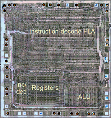
I have been reverse-engineering the Z-80 processor using images from the Visual 6502 team. The image below shows the overall structure of the Z-80 chip and the location of the ALU. The remainder of this article dives into the details of the ALU: its architecture, how it works, and exactly how it is implemented.
I've created the following block diagram to give an overview of the structure of the Z-80's ALU. Unlike Z-80 block diagrams published elsewhere, this block diagram is based on the actual silicon. The ALU consists of 4 single-bit units that are stacked to form a 4-bit ALU. At the left of the diagram, the register bus provides the ALU's connection to the register file and the rest of the CPU.
The operation of the ALU starts by loading two 8-bit operands from registers into internal latches. The ALU does a computation on the low 4 bits of the operands and stores the result internally in latches. Next the ALU processes the high 4 bits of the operands. Finally, the ALU writes the 8 bits of result (the 4 low bits from the latch, and the 4 high bits just computed) back to the registers. Thus, by doing two computation cycles, the ALU is able to process a full 8 bits of data. ("Full 8 bits" may not sound like much if you're reading this on a 64-bit processor, but it was plenty at the time.)
As the block diagram shows, the ALU has two internal 4-bit buses connected to the 8-bit register bus: the low bus provides access to bits 0, 1, 2, and 3 of registers, while the high bus provides access to bits 4, 5, 6, and 7. The ALU uses latches to store the operands until it can use them. The op1 latches hold the first operand, and the op2 latches hold the second operand. Each operand has 4 bits of low latch and 4 bits of high latch, to store 8 bits.
Multiplexers select which data is used for the computation. The op1 latches are connected to a multiplexer that selects either the low or high four bits. The op2 latches are connected to a multiplexer that selects either the low or high four bits, as well as selecting either the value or the inverted value. The inverted value is used for subtraction, negation, and comparison.
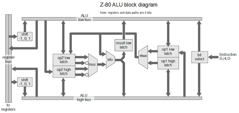
The two operands go to the "alu core", which performs the desired operation: addition, logical AND, logical OR, or logical XOR. The ALU first performs one computation on the low bits, storing the 4-bit result into the result low latch. The ALU then performs a second computation on the high bits, writing the latched low result and the freshly-computed high bits back to the bus. The carry from the first computation is used in the second computation if needed.
The Z-80 provides extensive bit-addressed operations, allowing a single bit in a byte to be set, reset, or tested. In a bit-addressed operation, bits 5, 4, and 3 of the instruction select which of the 8 bits to use. On the far right of the ALU block diagram is the bit select circuit that support these operations. In this circuit, simple logic gates select one of eight bits based on the instruction. The 8-bit result is written to the ALU bus, where it is used for the bit-addressed operation. Thus, decoding this part of an instruction happens right at the ALU, rather than in the regular instruction decode logic.
The Z-80's shift circuitry is interesting. The 6502 and 8085 have an additional ALU operation for shift right, and perform shift left by adding the number to itself. The Z-80 in comparison performs a shift while loading a value into the ALU. While the Z-80 reads a value from the register bus, the shift circuit selects which lines from the register bus to use. The circuit loads the value unchanged, shifted left one bit, or shifted right one bit. Values shifted in to bit 0 and 7 are handled separately, since they depend on the specific instruction.
The block diagram also shows a path from the low bus to the high op2 latch, and from the high bus to the low op1 latch. These are for the 4-bit BCD shifts RRD and RLD, which rotate a 4-bit digit in the accumulator with two digits in memory.
Not shown in the block diagram are the simple circuits to compute parity, test for zero, and check if a 4-bit value is less than 10. These values are used to set the condition flags.
The silicon that implements the ALU
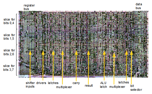
The image above zooms in on the ALU region of the Z-80 chip. The four horizontal "slices" are visible. The organization of each slice approximately matches the block diagram. The register bus is visible on the left, running vertically with the shifter inputs sticking out from the ALU like "fingers" to obtain the desired bits. The data bus is visible on the right, also running vertically. The horizontal ALU low and ALU high lines are visible at the top and bottom of each slice. The yellow arrows show the locations of some ALU components in one of the slices, but the individual circuits of the ALU are not distinguishable at this scale. In a separate article, I zoom in to some individual gates in the ALU and show how they work: Reverse-engineering the Z-80: the silicon for two interesting gates explained.
The ALU's core computation circuit

The heart of each bit of the ALU is a circuit that computes the sum, AND, OR, or XOR for two one-bit operands. Zooming in shows the silicon that implements this circuit; at this scale the transistors and connections that make up the gates are visible. Power, ground, and the control lines are the vertical metal stripes. The shiny horizontal bands are polysilicon "wires" which form the connections in the circuit as well as the transistors. I know this looks like mysterious gray lines, but by examining it methodically, you can figure out the underlying circuit. (For details on how to figure out the logic from this silicon, see my article on the Z-80's gates.) The circuit is shown in the schematic below.

This circuit takes two operands (op1 and op2), and a carry in. It performs an operation (selected by control lines R, S, and V) and generates an internal carry, a carry-out, and the result.
ALU computation logic in detail
The first step is the "carry computation", which is done by one big multi-level gate. It takes the two operand bits (op1 and op2) and the carry in, and computes the (complemented) internal carry that results from adding op1 plus op2 plus carry-in. There are just two ways this sum can cause a carry: if op1 and op2 are both 1 (bottom AND gate); or if there's a carry-in and at least one of the operands is a 1 (top gates). These two possibilities are combined in the NOR gate to yield the (complemented) internal carry. The internal carry is inverted by the NOR gate at the bottom to yield the carry out, which is the carry in for the next bit. There are a couple control lines that complicate carry generation slightly. If S is 1, the internal carry will be forced to 0. If R is 1, the carry out will be forced to 0 (and thus the carry in for the next bit).The multi-level result computation gate is interesting as it computes the SUM, XOR, AND or OR. It takes some work to step through the different cases, but if anyone wants the details:
- SUM: If R is 0, S is 0, and V is 0, then the circuit generates the 1's bit of op1 plus op2 plus carry-in, i.e. op1 xor op2 xor carry-in. To see this, the output is 1 if all three of op1, op2, and carry-in are set, or if at least one is set and there's no internal carry (i.e. exactly one is set).
- XOR: If R is 1, S is 0, and V is 0, then the circuit generates op1 xor op2 To see this, note that this is like the previous case except carry-in is 0 because of R.
- AND: If R is 0, S is 1, and V is 0, then the circuit generates op1 and op2. To see this, first note the internal carry is forced to 0, so the lower AND gate can never be active. The carry-in is forced to 1, so the result is generated by the upper AND gate.
- OR: If R is 1, S is 1, and V is 1, then the circuit generates op1 or op2. The internal carry is forced to 0 by S and the the carry-out (carry-in) is forced to 0 by R. Thus, the top AND gate is disabled, and the 3-input OR gate controls the result.
Believe it or not, this is conceptually a lot simpler than the 8085's ALU, which I described in detail earlier. It's harder to understand, though, then the 6502's ALU, which uses simple gates to compute the AND, OR, SUM, and XOR in parallel, and then selects the desired result with pass transistors.
Conclusion
The Z-80's ALU is significantly different from the 6502 or 8085's ALU. The biggest difference is the 6502 and 8085 use 8-bit ALUs, while the Z-80 uses a 4-bit ALU. The Z-80 supports bit-addressed operations, which the 6502 and 8085 do not. The Z-80's BCD support is more advanced than the 8085's decimal adjust, since the Z-80 handles addition and subtraction, while the 8085 only handles addition. But the 6502 has more advanced BCD support with a decimal mode flag and fast, patented BCD logic.If you've designed an ALU as part of a college class, it's interesting to compare an "academic" ALU with the highly-optimized ALU used in a real chip. It's interesting to see the short-cuts and tradeoffs that real chips use.
I've created a more detailed schematic of the Z-80 ALU that expands on the block diagram and the core schematic above and shows the gates and transistors that make up the ALU.
I hope this exploration into the Z-80 has convinced you that even with a 4-bit ALU, the Z-80 could still do 8-bit operations. You didn't get ripped off on your old TRS-80.
Credits: This couldn't have been done without the Visual 6502 team especially Chris Smith, Ed Spittles, Pavel Zima, Phil Mainwaring, and Julien Oster.
23 comments:
There is an issue with the layout of the OR gate that takes V and the internal carry as inputs: I don't think it should be connected to op2.
(I meant op1, not op2, sorry)
Anonymous: yes, that line is positioned ambiguously; it should be connected to the top OR gate, not the bottom one. I have a hard time drawing multi-level gates with Eagle.
Can you explain why the op latches have bidirectional connections to the ALU low bus and ALU high bus? Do the values here need to get read out without going thru the ALU in some circumstances?
In your detailed schematic, the bit select logic seems wrong. You are showing bits 1 and 5, shouldn't it be bits 2 and 6?
Anonymous, I'm glad my schematic is getting studied in detail. I think the bit select logic on the far right is correct. The upper NOR gate is active if /i5 is 1, /i4 is 0, and /i3 is 1, i.e. the instruction is xx010xxx, which is 2. The lower NOR gate is active if /i5 is 0, /i4 is 0, and /i3 is 1, i.e. instruction xx110xxx, which is 6.
On bitslice 0 of the ALU, is Carry In set to S so that the XOR works correctly on that bit of the word?
(I guess it's S OR Cin from previous ALU operation).
I haven't figured out the carry-in circuit yet, but based on the 8085 Regarding the carry in: I haven't figured out that circuit yet. I expect it to be slightly complicated since it depends on the instruction (e.g. add vs add with carry need different inputs).
In the 8085 the carry-in also needs to be set appropriately for rotate left and rotate left through carry. Since the Z-80 does rotates differently, that won't be the case.
This is very cool - both how the 8-bit CPU actually has a 4-bit ALU, and the fact that you've reverse-engineered it all by staring at photos of the silicon. I'm in the midst of designing my own custom 4-bit CPU from 7400 logic, so it's interesting to see another relevant example.
I thought I knew the ins and outs of the venerable CPU, but you proved me wrong. Well done, nice work!
What about the 16-bits operations? Are they executed as four 4-bits operations?
R.
Ken,
I see it now, I misread the double inversion logic. This and the 8085 teardown are excellent. I am looking forward to implementing this in an FPGA, then optimizing it for performance instead of the original need for minimal gate count. BTW: I started designing PCs based on the NEC uPD780 more than thirty years ago, at NEC. The Z80 still is my favorite. No longer Anonymous.
Very interesting stuff, indeed.
BTW, did you find in the layout any of the transistor traps (fake, always on, depletion mode transistors intended to dificult reverse ingeeniering) Masatoshi Shima mentioned?
It doesn't surprise me that its a 4bit ALU:
I wrote this in 1989, I didn't have access to the silicon implementation but to keep the half carry it made sense that it should be so.
addr3toA: ; subroutine to add r3 to reg_A
extzv #0, #4, r3, r4 ; get lower nibble in r3
extzv #0, #4, reg_A, r6 ; get lower nibble of A in r6
addb2 r4, r6 ; add lower nibbles
cmpb r6, #^x0F
bleq no_H1 ; branch if no Half Carry
bisb2 #^x10, reg_F ; set H_flag
no_H1:
addb2 r3, reg_A ; do add set vax flags
movpsl r2
blbc r2, 31$
bisb2 #^x01, reg_F ; set C flag
31$: bbc #1, r2, 32$
bisb2 #^x04, reg_F ; set V flag
32$: bbc #2, r2, 33$
bisb2 #^x40, reg_F ; set Z flag
33$: bbc $3, r2, 34$
bisb2 #^x80, reg_F ; set S flag
Most of 8-bit CPUs have an 8-bit ALU, so I don't understand what is the avvantage to use a 4-bit ALU to perform 8-bits operations.
Hi Ken,
Good job with the reverse engineering. I really like your articles about the z80.
You stated that "Not shown in the block diagram are the simple circuits to compute parity, test for zero, and check if a 4-bit value is less than 10. These values are used to set the condition flags."
Can you please explain how the zero flag is generated? I suppose it is a NOR of all the bits. But since the ALU is 4-bits is the zero flag generated from the 8-bit result? or is it generated from each nibble and then put together, like if there was a "half"-zero flag.
Please keep writing articles about z80 :D Thank you
good job ! it allowed me to implement this ALU using minecraft redstone.
However, by doing this, I found a few mistakes :
1)the last gate should be a OR gate instead of a NOR.
2)to perform a OR computation, R=0 (and not 1 as mentionned), S=1 and V=1.
It's been mentioned a few times that other CPUs such as the 6502 have 8-bit ALUs.
The 6502 ALU is actually a pair of 4-bit ALUs daisy chained together.
You could say the Z80's processing path that requires a second lap through its 4-bit ALU via latches to handle larger words (or three additional laps for a 16-bit word) is simply unrolled one lap in the 6502's silicon to achieve an 8-bit unit. The 6502 would face some additional challenges also were it to have had a monolithic 8-bit ALU since the paired 4-bit nybble ALUs provided an intermediary half-carry on the first nybble that permits a fast carry decider (multiplexed between binary/bcd carry) and fast decimal adjust on the low-order nybble for its patented BCD optimization to work the way it does. With a monolithic 8-bit design the decimal adjustment would have had to have been done in a separate stage to the full 8-bit add/sub output consuming additional cycles.
This post was old. I'm not sure if someone will read this and answer me.
Well, Your image schematics is very helpful
your pdf schematics is seems to be helpful.
But I don't understand it.
(Also I come to find just a logic gate schematic)
(i) how does ALU bus select its bit
(ii) What is that op amp with S gate there
(iii) Can you implement me some pin we will have and what does them do
Thx for all answer soon.
Well Unknown, I think its not mistake. Its base on silicon which have nor gate and have no or gate
> (ii) What is that op amp with S gate there
Maybe a “superbuffer”. I just read that term on http://www.righto.com/2020/10/how-bootstrap-load-made-historic-intel.html#fn:circuits , although that's on a different processor.
It seems to make sense because these appear everywhere a bus has to be driven by a regular gate.
The 8080 can do 8-bit ALU operations in 1T and it would be strange if the Z80 is slower, as both were designed by the same people.
The big question for me is how much can the Z80 ALU do in 1T? Is it two 4-bit operations or only one?
P.S.
Ken says the WZ is invisible to the programmer. This is true for the 8080, however bits 5 & 3 of the Z80 W are copied to the same bits in F after BIT b,(HL). Also, CPI/CPD increment/decrement WZ, so that WZ[13:0] can be known for certain.
A Sinclair ZX81 owner thanks you many times!
Post a Comment