Christmas shopping the IBM way: computerized gift selection in 1962

In 1962, the Simpson's department store in Toronto used an IBM computer to help customers select Christmas gifts, based on the characteristics of the recipients.1 I came across a video that shows how it worked.

"Now! A computer makes Christmas shopping easier." The IBM 1401 computer is the cabinet at the back, with the 1403 printer to the right of it. The 1402 card reader is at the left and the 729 tape drives at the right, (Click for a larger version.) Advertisement in The Financial Post, November 24, 1962.

"Now! A computer makes Christmas shopping easier." The IBM 1401 computer is the cabinet at the back, with the 1403 printer to the right of it. The 1402 card reader is at the left and the 729 tape drives at the right, (Click for a larger version.) Advertisement in The Financial Post, November 24, 1962.

The IBM 1401 computer (below) was pre-programmed with 3000 categorized gifts.2 A customer described the gift recipient: their age range, their interests, their gender (male, female, or couple), the gift category (e.g. apparel, personal, or "the man who has everything"), and the price range (ranging from $5 to "money is no object").

The IBM 1401 computer at Simpson's department store in 1962. The computer is barely visible behind the man's head. The 1402 card reader is at the left. Still from CBC video.

The IBM 1401 computer at Simpson's department store in 1962. The computer is barely visible behind the man's head. The 1402 card reader is at the left. Still from CBC video.

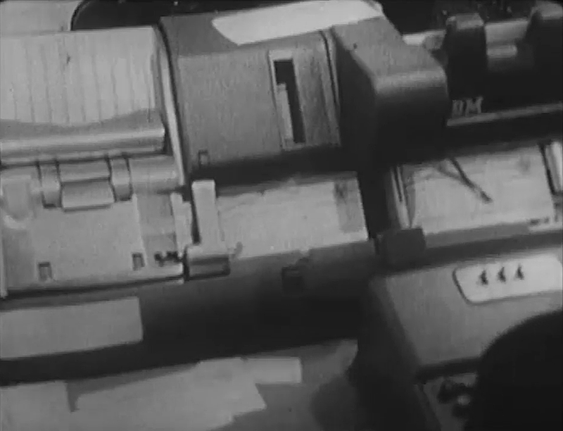
This information was punched onto a card by an operator (called a "girl" in the interview) using an IBM 26 keypunch, as shown below.

Entering the customer data into the IBM 26 keypunch. Still from CBC video.

Entering the customer data into the IBM 26 keypunch. Still from CBC video.

After running the card through the computer, a gift list with ten suggestions was printed on the IBM 1403 line printer. The list was torn off and given to the customer to help with their shopping.

Removing the Christmas shopping list from the IBM 1403 line printer. The Simpson's logo is barely visible in the upper left corner. Still from CBC video.

Removing the Christmas shopping list from the IBM 1403 line printer. The Simpson's logo is barely visible in the upper left corner. Still from CBC video.

The gift suggestions included a King James bible, Eskimo soapstone, a leather-covered cigarette case, Cossack boots, a Marabou-trim bed jacket, Roto-Shine electric shoe polisher ($26.95), a table lighter in the design of an antique pistol ($4.95), a soda siphon ($15.95) "a little more expensive, probably for your father or your husband", an electrified magnifying glass "to read the stock market report" ($7.95), or moccasins trimmed with seal fur ($6.95). (Gift ideas seem to have changed drastically since the 1960s.)

The interviewer suggested that this computer might take all the fun out of Christmas shopping and called it a "Santa monster", but the operator insisted that most people need some help with their shopping. It must have been an unusual experience for people to encounter a computer in person back then, but this gift computer was very popular, with 2000 people a day using it.

I announce my latest blog posts on Twitter, so follow me @kenshirriff. I also have an RSS feed. Thanks to Tim and Lisa Robinson for tracking down the newspaper clipping.

Notes and references

  1. The video is Christmas Shopping the IBM Way, broadcast on CBC on Dec 18, 1962. The host was Anna Cameron with guest Brian Finney. (Only the first part of the video shows the computer system; most of the video discusses the gift choices in detail.) The system was also discussed in a CBC Radio segment, Christmas Computer Selects the Perfect Gift, reported by Jim McLean and Joelle Pearson on Dec 4, 1962. The radio interview also discusses the use of the system at Gimbel's department store in New York. 

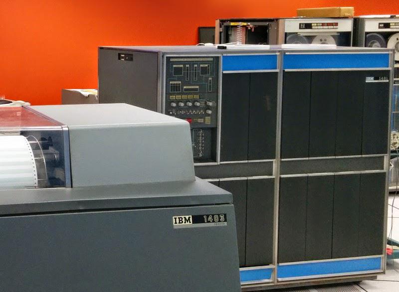
  2. The IBM 1401 computer is just barely visible in the video, so here's a photo that shows an IBM 1401 computer more clearly.

    An IBM 1401 computer. The line printer (1403) is in the foreground, while IBM 729 tape drives are in the background. This computer is at the Computer History Museum.

    An IBM 1401 computer. The line printer (1403) is in the foreground, while IBM 729 tape drives are in the background. This computer is at the Computer History Museum.


Reverse-engineering a tiny 1980s chip that plays Christmas tunes

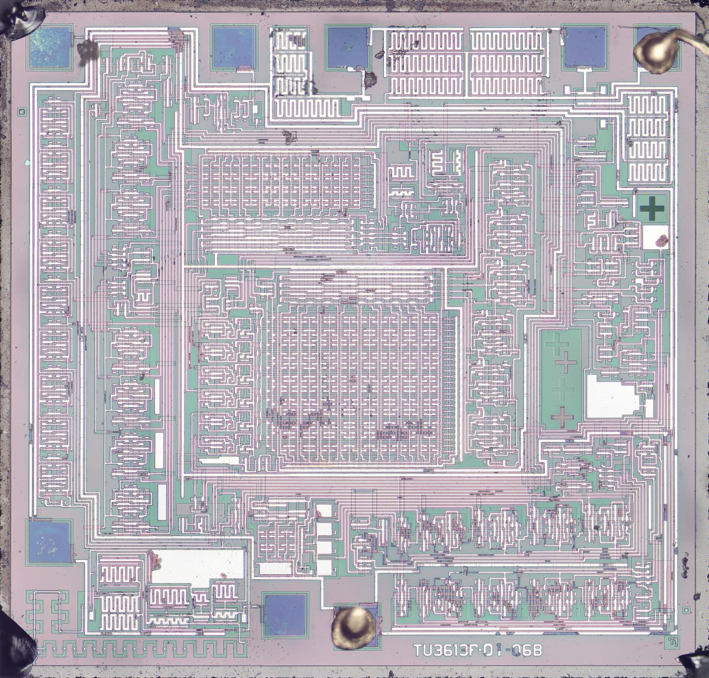
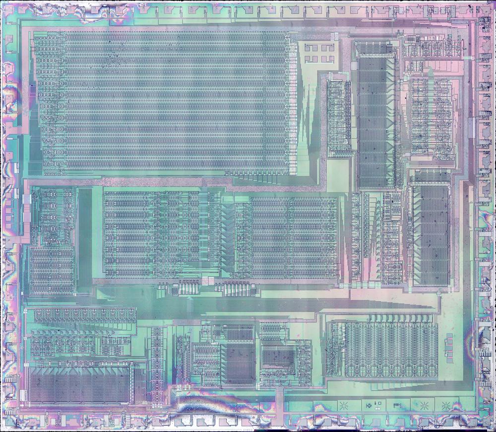
For the holidays, I decapped a chip that plays three Christmas melodies. The UM66T melody chip from the 1980s was designed for applications such as greeting cards and toys. It looks like a transistor, but when connected to a battery and speaker it plays music. The die photo below shows the tiny silicon chip that I reverse engineer in this blog post.

The UM66T die under the microscope. Click this (or any other) image for a larger version.

The UM66T die under the microscope. Click this (or any other) image for a larger version.

The video below shows the chip in action. Click to hear the chip play Jingle Bells, Santa Claus is Coming to Town, and We Wish You a Merry Christmas.

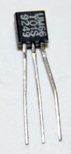
The chip is packaged in a 3-pin package that looks like a transistor (below). I dissolved the epoxy package in boiling sulfuric acid to expose the silicon die inside. This was my first acid decap and it turned out okay, although there are some scratches on the die. The composite photo above shows the CMOS chip under the microscope. The features are fairly large, even for the time; the metal traces are about 3.3µm wide and the silicon about 5.4µm.

The chip is in a 3-pin TO-92 package, like a transistor.

The chip is in a 3-pin TO-92 package, like a transistor.

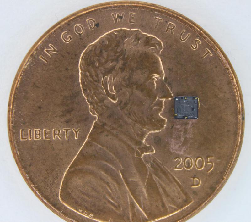
The silicon die is very small, about 1.8mm×1.8mm. The photo below gives an idea of the scale.

The UM66T die on top of a penny.

The UM66T die on top of a penny.

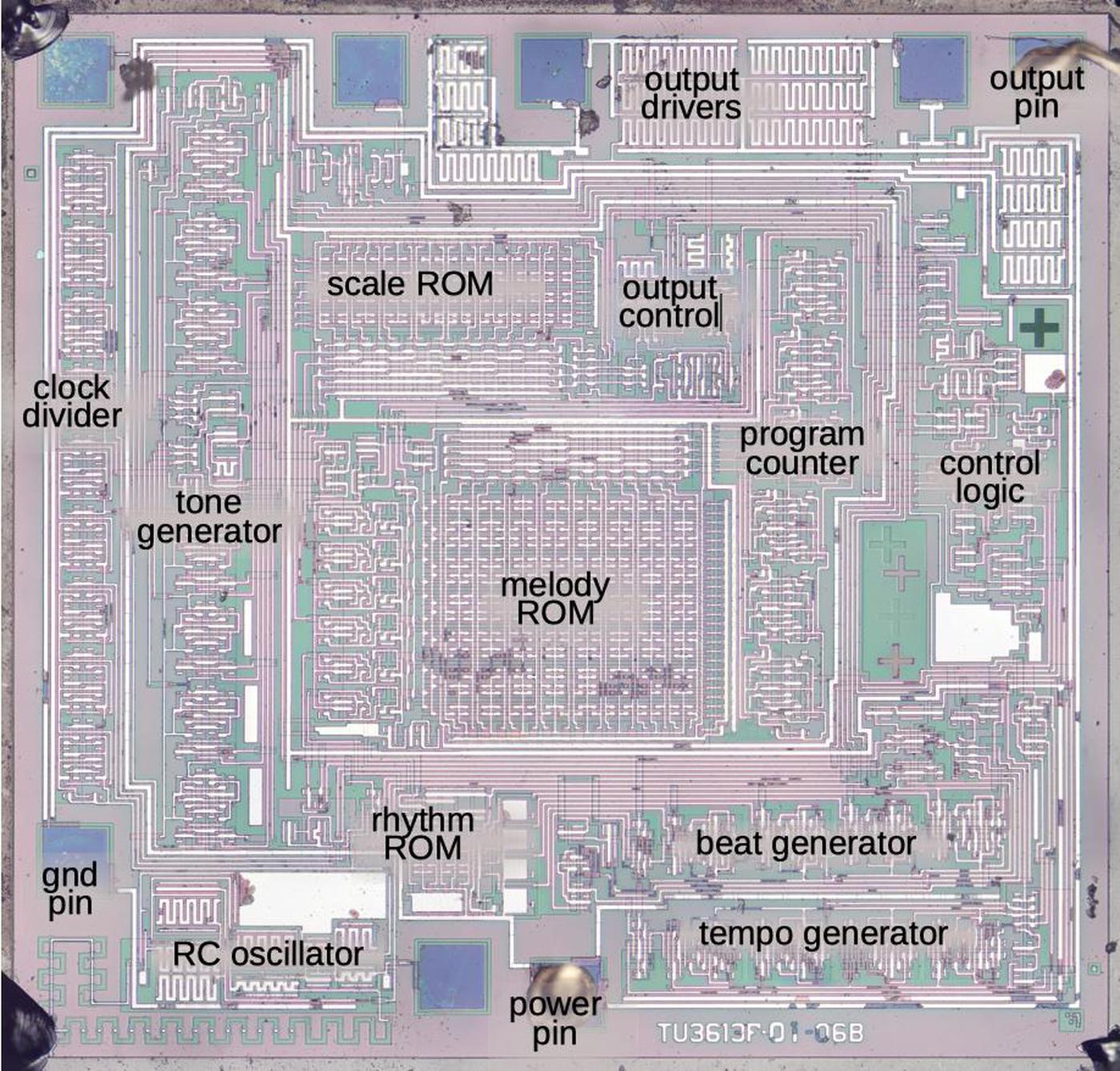
I've labeled the die photo with the functional blocks. The melody chip is an optimized, minimal design. It is constructed from flip-flops and gates, not the microcontroller you might expect.

Die photo of the UM66T with the main functional blocks labeled.

Die photo of the UM66T with the main functional blocks labeled.

The chip has 3 pins, but there are 8 pads on the die. The other pins appear to be used for testing. By activating one of the pins, the chip can be put into a test mode. The test mode runs through the songs at 512× speed so the chip can be tested quickly without waiting for the tunes to play. The other test pins appear to expose other internal data for testing.

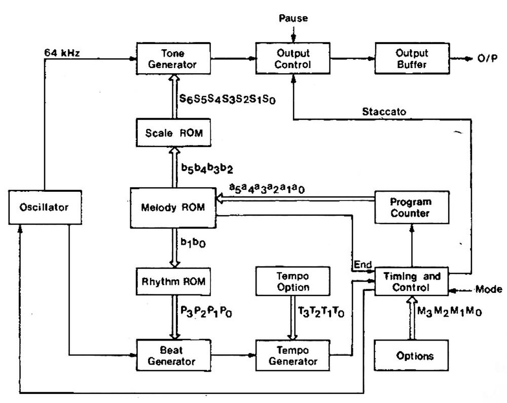
The block diagram below shows the structure of the chip. (Inconveniently, I didn't get this diagram until after I'd reverse-engineered the circuitry.) The basic idea is that the "program counter" steps through the 64 notes stored in the melody ROM. Four bits form the note pitch index, while two bits select the note duration. The Scale ROM and tone generator are used to convert the pitch index into the desired output tone. Meanwhile, the Rhythm ROM converts the 2-bit note duration into a 4-bit value indicating how long the note is.

Block diagram of the UM66T. From Maplin Magazine, March 1988.

Block diagram of the UM66T. From Maplin Magazine, March 1988.

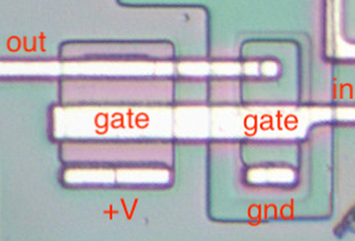
The chip is built from CMOS, like most modern ICs. The photo below shows an inverter: a PMOS transistor on the left and an NMOS transistor on the right. The PMOS one turns on with a 0 input, pulling the output high. The NMOS transistor turns on with a 1, pulling the output low. Thus, the two transistors implement the desired inverter behavior.

Structure of an inverter.

Structure of an inverter.

The melody ROM

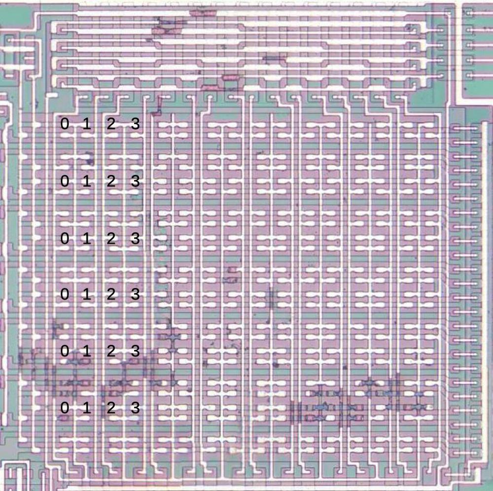
The 64 notes are stored in a 64×6 ROM, shown below. Each note is 4 bits for the frequency and 2 bits for the duration of the note. The ovals are the transistor gates; bits are stored in the wiring pattern of the transistors, either to the left or to the right. The vertical column select lines from the top select one column in the ROM. The vertical lines from the bottom, however, inactivate the transistor.

Physically, the ROM stores four notes in each column, so it has 16 columns of 24 bits. At the top of the ROM is a binary decoder that energizes one of the 16 columns, based on the input value. The transistors at the left of the ROM select one bit out of each four to produce the desired 6-bit word. The 6 bits are latched. Then 4 bits are used to generate the desired note frequency, while two bits select the duration of the note (half note, quarter note, or eighth note).

The melody ROM holds 64 notes.

The melody ROM holds 64 notes.

In the diagram above, the numbers show the locations of the first four words. The first word is 000100, a start code. The next two words are 011100; 0111 indicates the note E5 and 00 indicates a short duration.1 The next word is by 011101, indicating a longer E5. Thus, the indicated words store the first three notes of "Jingle Bells".

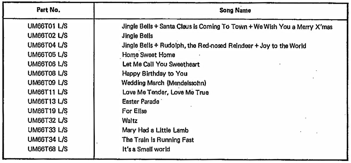
The metal layer of an IC can be changed relatively easily. By changing the metal layer, different versions of the chip could be manufactured with different ROMS, producing different songs. (The chip could also be manufactured with different note ranges, tempo, and beats, providing more flexibility.) The table below shows the songs that were available.2

List of songs available in the UM66T chip line. From the datasheet.

List of songs available in the UM66T chip line. From the datasheet.

Generating the note frequency

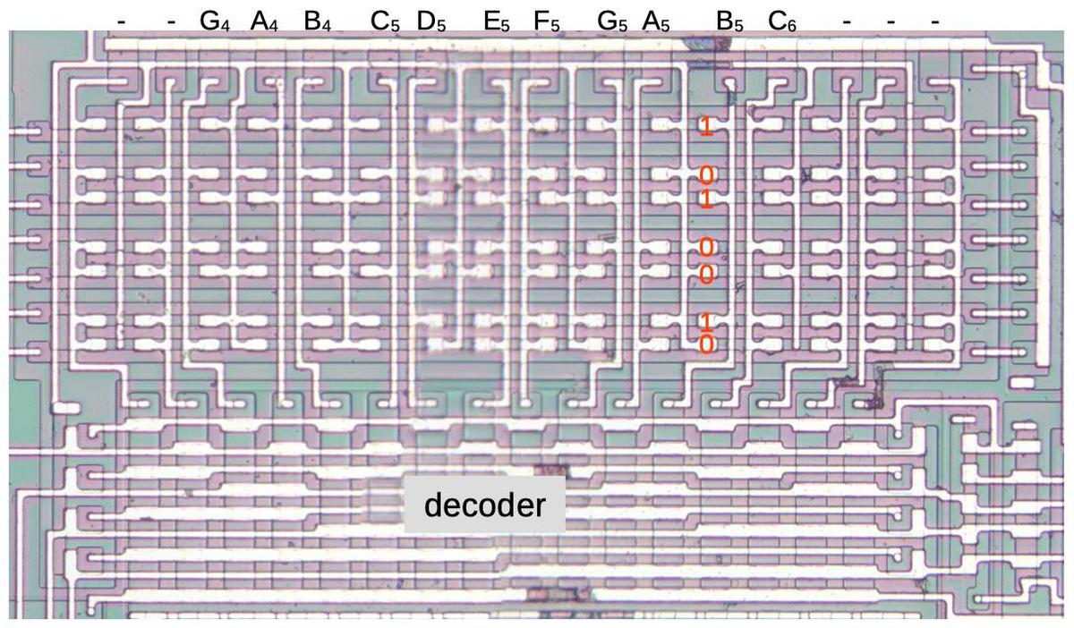
The melody ROM doesn't specify the note's frequency directly, but instead has a value from 0 to 15. A second ROM, the scale ROM, has the mapping to convert the note value into a frequency. Specifically, the output frequency is 32768÷N, where N is the value in the scale ROM. The frequency resolution from this isn't great, so some notes are noticeably out of tune, but it's good enough for this application.

The note frequency ROM.

The note frequency ROM.

The image above shows the scale ROM, configured to produce the notes G4 through C6 in the key of C. (Different versions of the chip can generate different notes by changing the scale ROM.) As with the melody ROM, the binary values are generated by the wiring of the metal layer to the transistors. For instance, the note B5 has the bits 0,1,0,0,1,0,1 (from bottom to top). Below the ROM, the decoder activates one of the 16 column lines based on the 4-bit note value. (Notice the binary pattern of transistors in the decoder: the top rows alternate, the next rows are every 2, then every 4 and every 8.

The chip uses an unusual technique to generate the output frequency. The standard way is to divide the clock frequency by the scale factor with a counter, but instead the chip has an unusual approach to save a few transistors. It uses a 7-bit linear-feedback shift register. The construction of the linear-feedback shift register is that the input is the XOR of the last two bits. It will cycle pseudo-randomly through all 127 values.4

The trick in the melody chip is to initialize the shift register with a particular value loaded from the ROM, and run through the sequence until the value 1000000 is reached. By picking the right starting value, the desired number of counts will be obtained. The diagram below illustrates the operation of the shift register with the B5 input 0100101. With this starting value, it takes 34 steps to reach the final value of binary 1000000. Notice how the bits are shifted to the right each step, with a new bit inserted at the left.

0 1 0 0 1 0 1
1 0 1 0 0 1 0
1 1 0 1 0 0 1
1 1 1 0 1 0 0
0 1 1 1 0 1 0
1 0 1 1 1 0 1
1 1 0 1 1 1 0
1 1 1 0 1 1 1
0 1 1 1 0 1 1
0 0 1 1 1 0 1
1 0 0 1 1 1 0
1 1 0 0 1 1 1
0 1 1 0 0 1 1
0 0 1 1 0 0 1
1 0 0 1 1 0 0
0 1 0 0 1 1 0
1 0 1 0 0 1 1
0 1 0 1 0 0 1
1 0 1 0 1 0 0
0 1 0 1 0 1 0
1 0 1 0 1 0 1
1 1 0 1 0 1 0
1 1 1 0 1 0 1
1 1 1 1 0 1 0
1 1 1 1 1 0 1
1 1 1 1 1 1 0
1 1 1 1 1 1 1
0 1 1 1 1 1 1
0 0 1 1 1 1 1
0 0 0 1 1 1 1
0 0 0 0 1 1 1
0 0 0 0 0 1 1
0 0 0 0 0 0 1
1 0 0 0 0 0 0

Since this takes 34 steps, the clock frequency is divided by 34 and the output frequency is 32768 ÷ 34 = 963 Hertz, close to the desired frequency of 997 Hertz.3 For another example, G4 starts with 1001010 and runs for 84 counts, yielding a frequency of 392 Hertz. Thus, the ROM controls the frequency of the notes produced. Note that the starting values are not obviously correlated with the frequency; they depend on the sequence generated by the linear feedback shift register. (This sequence is called pseudo-random since it is deterministic but appears kind of random.)

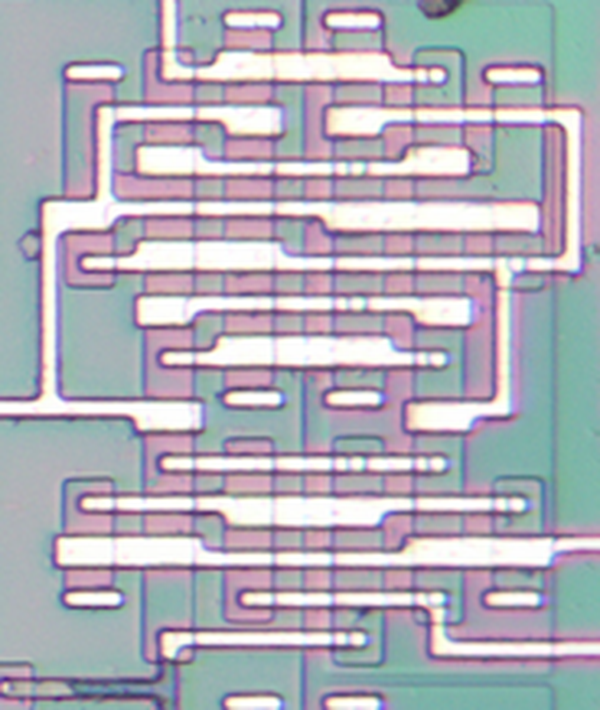
Next, I'll discuss the implementation of the shift register. The die photo below shows one stage of the shift register. It receives input from the stage below and passes its output to the stage above. The stage is constructed from 26 transistors: 13 PMOS transistors on the left and 13 NMOS transistors on the right. The transistors are oriented vertically along the pink regions of doped silicon. The transistor gates are where the metal lines widen. Note that transistors in a column are connected by the silicon.

Die photo showing one stage of the shift register.

Die photo showing one stage of the shift register.

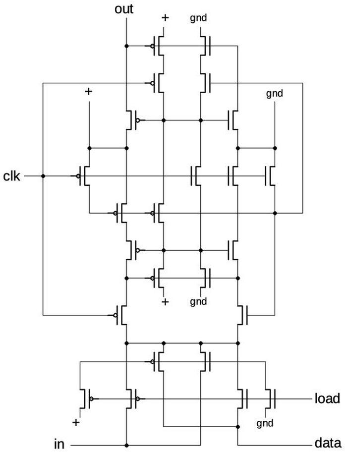
The schematic below shows how the transistors are connected, corresponding to the die photo above.

Schematic of one stage of the shift register, corresponding to the die photo.

Schematic of one stage of the shift register, corresponding to the die photo.

At a slightly higher level, the circuit consists of inverters and multiplexers5 as shown below. Each loop of two inverters holds a bit. The first multiplexer selects the input: either a value from the ROM that is loaded into the shift register, or the value from the previous stage. When the clock goes high, this value is loaded into the first inverter loop. When the clock goes low, the value in the first inverter loop is transferred to the second inverter loop, and thus the output. Thus, it takes one complete clock cycle (low then high) to shift a bit one stage in the shift register.

Schematic of one stage of the shift register.

Schematic of one stage of the shift register.

The clock

The chip runs on a 64-kilohertz clock. This clock is generated from a simple resistor-capacitor-inverter oscillator inside the chip, avoiding the need for external components. Because the capacitor takes some time to charge through the resistor, the oscillation speed is controlled.

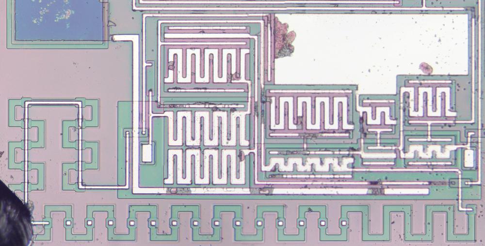
The die photo below shows a closeup of the oscillator. The white rectangle is the capacitor. The green zig-zag is the resistor. Note that the resistance can be adjusted by shorting out part of the resistor in the metal layer. The white zig zags are the gates of the inverter transistors. These transistors are larger than the typical logic transistors.

Die photo showing the clock circuitry.

Die photo showing the clock circuitry.

The on-chip R-C oscillator is cheap but inaccurate, unlike a quartz crystal oscillator. If the voltage changes, the frequency changes. In the video below, I lower and raise the voltage, and you can hear the effect on the tunes as the frequency changes.

Timing

The 64-kilohertz clock goes through a divider chain to divide the frequency by 512. This divider is made of nine toggle flip-flops, each one dividing the frequency by 2. These flip-flops are built from inverters and multiplexers similar to the shift register flip-flops, but wired to toggle. This feeds the beat generator, which adjusts the timing for quarter notes, eighth notes, etc. It uses a linear-feedback shift register, similar to the tone generator, but with four shift register stages. The shift register is loaded with a value from the rhythm ROM that determines the length of the note.

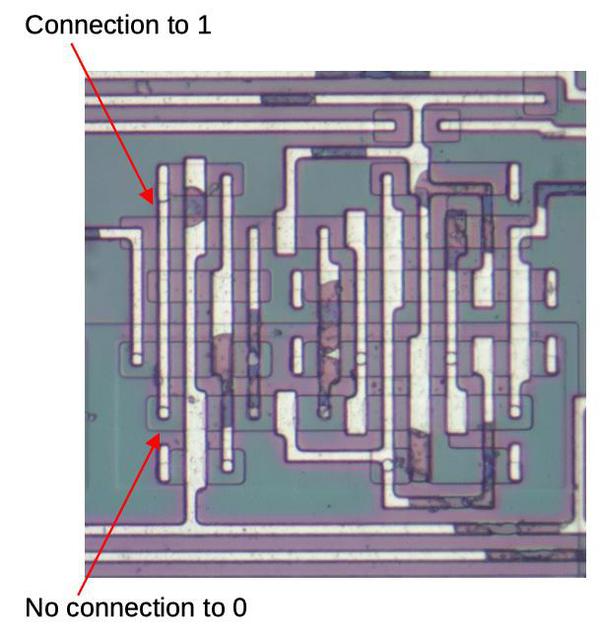
The output from the beat generator goes to the tempo generator, which divides its input by a preset amount (1 to 15) to generate a tempo between 128 and 1920 beats per minute. The tempo generator is also a 4-bit linear feedback shift register. The input to the shift register is hard wired to set the fixed tempo. The photo below shows one stage, wired to 1. A small change to the metal layer would cause 0 to be connected instead of 1.

The tempo is programmed by wiring shift register inputs to either 0 or 1.

The tempo is programmed by wiring shift register inputs to either 0 or 1.

The program counter counts through the 64 notes, providing the address to the melody ROM. It is built from toggle flip-flops chained together to build a 6-bit counter. The flip-flops have a reset line to initialize the counter to 0 at the start. The chip has a few dozen logic gates to keep track of the current state, handle startup, test mode, and so forth.

Conclusion

This melody chip uses simple circuits to produce songs in a flexible way. The chip integrates all the necessary circuitry including the R-C oscillator, so only a battery and a speaker were required. Nowadays a microcontroller would be the easiest way to implement this. This 1980s chip, however, uses small ROMS and simple counters to produce the tunes. I'll end with a quote from John Nolan: "Nothing says 'Christmas' like decapitating a microchip that plays slightly off-key Christmas songs."

This article is the extension of my earlier Twitter thread, which had a bunch of discussion on Hacker News. I announce my latest blog posts on Twitter, so follow me @kenshirriff. I also have an RSS feed. Thanks to Mark Fraser for finding an article on the chip.6

Notes and references

  1. The note codes range from 0010 for G4 through 1100 for C6, in the key of C. I wrote a short Python program to convert the ROM contents to notes. 

  2. Datasheets for the UM66T are available here, here, and here. A die photo of a different UM66T version is on siliconpr0n; I think this one plays Für Elise. 

  3. The output frequency is half what you might expect from the 64 kHz clock. To keep the waveform symmetrical, there is a toggle flip-flop on the output that divides the counter output by 2. 

  4. The 7-bit LFSR has 127 values instead of 128 values because it will get stuck in the all-zero value (since 0⊕0 = 0). 

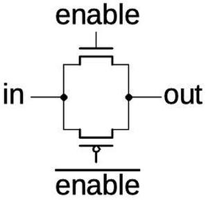
  5. The multiplexers are built from a CMOS circuit called a transmission gate (below). A transmission gate operates as a switch. When enable is high, both transistors turn on, passing the signal through the gate. When enable is low, both transistors turn off, blocking the signal. (Note that the PMOS transistor has an inverted control signal.) A multiplexer is built from two transmission gates. The control signal is connected to the two transmission gates with opposite polarity, so one transmission gate will be active at a time. Thus, one of the inputs is selected.

    Schematic of a transmission gate.

    Schematic of a transmission gate.


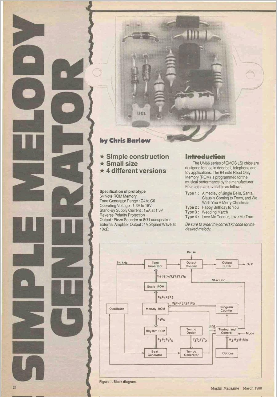
  6. A 1988 article (p24-26) in Maplin Electronics described how to build a circuit with the UM66T.

    First page of the article from Maplin Electronics, March 1988.

    First page of the article from Maplin Electronics, March 1988.


Yamaha DX7 chip reverse-engineering, part 4: how algorithms are implemented

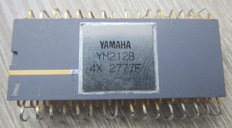
The Yamaha DX7 digital synthesizer (1983) was the classic synthesizer in 1980s pop music. It uses two custom digital chips to generate sounds with a technique called FM synthesis, producing complex, harmonically-rich sounds. Each note was implemented with one of 32 different patterns of modulation and summing, called algorithms. In this blog post, I look inside the sound chip and explain how the algorithms were implemented.
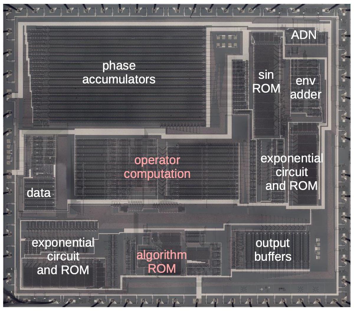
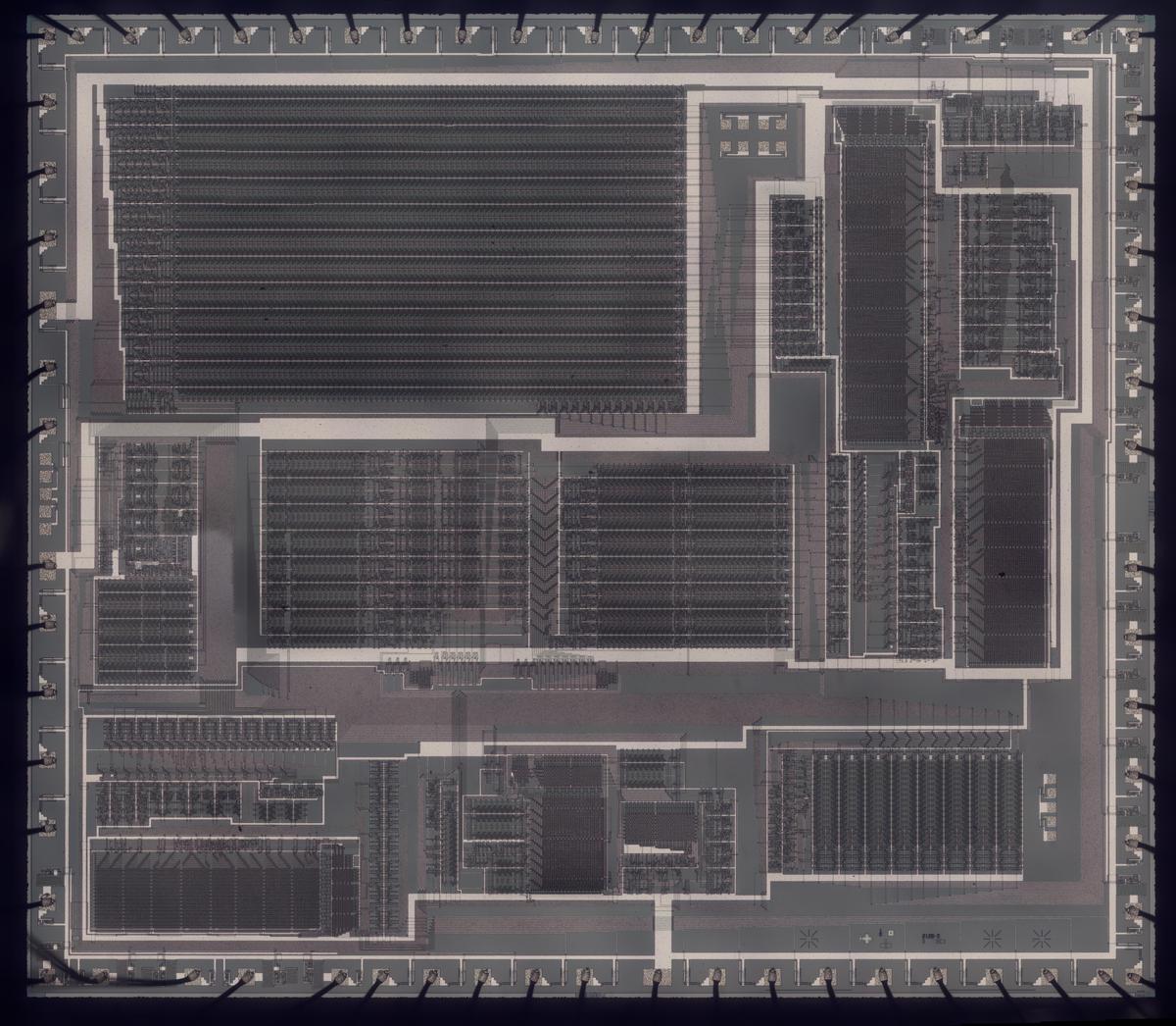
Die photo of the YM21280 chip with the main functional blocks labeled. Click this photo (or any other) for a larger version.

Die photo of the YM21280 chip with the main functional blocks labeled. Click this photo (or any other) for a larger version.

The die photo above shows the DX7's OPS sound synthesis chip under the microscope, showing its complex silicon circuitry. Unlike modern chips, this chip has just one layer of metal, visible as the whitish lines on top. Around the edges, you can see the 64 bond wires attached to pads; these connect the silicon die to the chip's 64 pins. In this blog post, I'm focusing on the highlighted functional blocks: the operator computation circuitry that combines the oscillators, and the algorithm ROM that defines the different algorithms. I'll outline the other functional blocks briefly. Each of the 96 oscillators has a phase accumulator used to generate the frequency. The sine and exponential functions are implemented with lookup tables in ROMs. Other functional blocks apply the envelope, hold configuration data, and buffer the output values.

The DX7 was the first commercially successful digital synthesizer, using a radically new way of generating sounds. Instead of the analog oscillators and filters of an analog synthesizer, the DX7 generates sounds digitally, using a technique called FM synthesis. The idea is that you start with a sine wave (the carrier signal) and perturb it with another signal (the modulating signal). The modulating signal changes the phase (and thus the frequency) of the carrier, creating complex harmonic structures. The custom chips inside the DX7 made this possible at an affordable price.

The DX7 synthesizer. Photo by rockheim (CC BY-NC-SA 2.0).

The DX7 synthesizer. Photo by rockheim (CC BY-NC-SA 2.0).

FM synthesis

I'll briefly explain how FM synthesis is implemented.1 The DX7 supports 16 simultaneous notes, with 6 operators (oscillators) for each note, 96 oscillators in total. However, to minimize the hardware requirements, the DX7 only has a single digital oscillator circuit. This circuit calculates each operator individually, in sequence. Thus, it takes 96 clock cycles to update all the sounds. To keep track of each oscillator, the DX7 stores 96 phase values, an index into the sine wave table. By incrementing the index at a particular rate, a sine wave is produced at the desired frequency.

The idea of FM synthesis is to modulate the index into the sine wave table; by perturbing the index, the output sine wave is modified. The diagram below shows the effects of modulation. The top curve shows a sine wave, generated by stepping through the sine wave table at a fixed rate. The second curve shows the effects of a small amount of modulation, perturbing the index into the table. This distorts the sine wave, compressing and stretching it. The third curve shows the effects of a large amount of modulation. The index now sweeps back and forth across the entire table, distorting the sine wave unrecognizably. As you can see, modulation can produce very complex waveforms. These waveforms have a rich harmonic structure, yielding the characteristic sound of the DX7. (I made a webpage here where you can experiment with the effects of modulation.)

Modulation examples. The top sine wave is unmodulated. The middle wave has a small amount of modulation. The bottom wave is highly modulated.

Modulation examples. The top sine wave is unmodulated. The middle wave has a small amount of modulation. The bottom wave is highly modulated.

Algorithms

The above section illustrated how two oscillators can be combined with modulation. The DX7 extends this principle, generating a note by combining six oscillators through modulation and summing. It implements 32 different ways of combining these oscillators, illustrated below, and calls each one an algorithm. The different algorithms provide flexibility and variety in sound creation. Multiple levels of modulation create harmonically-rich sounds. On the other hand, multiple output operators allow different sounds to be combined. An electric piano sound, for example, could have one sound for the hammer thud, a second sound for the body of the tone, and a third sound for the ringing tine, all varying over time.
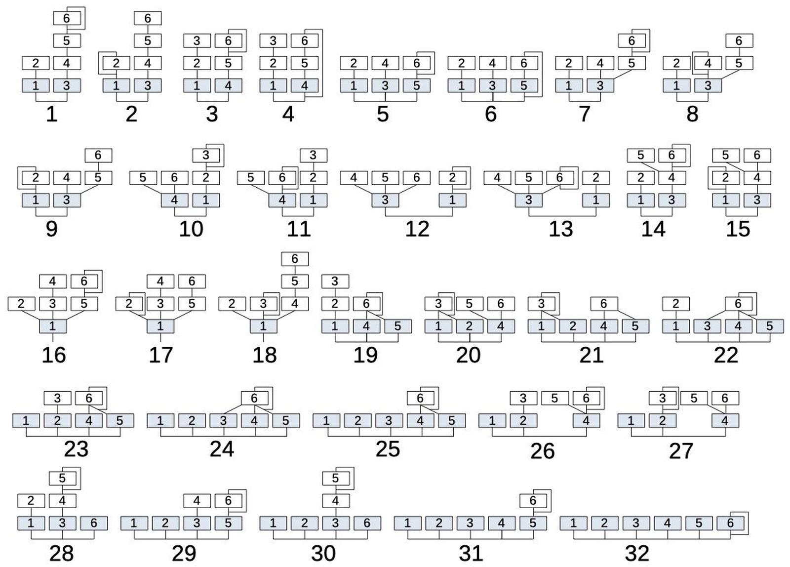
The 32 algorithms of the DX7 synthesizer.

The 32 algorithms of the DX7 synthesizer.

Looking at algorithm #8, for example, shows the structure of an algorithm. Each box represents an operator (oscillator). Operators 1 and 3 (in blue), are combined to form the output. The remaining operators provide modulation, as indicated by the lines. Operator 2 modulates operator 1. Operators 4 and 5 are combined to modulate operator 3, providing a complex modulation. Operator 6, in turn, modulates operator 5. Finally, the line looping around operator 4 indicates that operator 4 modulates itself. Since each modulation level can vary over time, the resulting sound can be very complex.
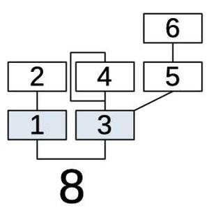
Algorithm 8 combines the six operators; two produce outputs.

Algorithm 8 combines the six operators; two produce outputs.

Shift-register storage

To understand the DX7's architecture, it's important to know that the chip uses shift registers, rather than RAM, for its storage. The idea is that bits are shifted from stage to stage each clock cycle. When a bit reaches the end of the shift register, it can be fed back into the register or a new bit can be inserted. For the phase accumulators, the shift registers are 96 bits long since there are 96 oscillators. Other circuits use 16 bit-shift registers to hold values for the 16 voices. The shift register circuitry (below) is dense, but even so, it takes up a large fraction of the chip.

A small part of the shift register storage.

A small part of the shift register storage.

The use of shift registers greatly affects the design of the DX7 chip. In particular, values cannot be accessed arbitrarily, as in RAM. Instead, values can only be used when they exit the shift register, which makes the circuit design much more constrained. Moreover, circuits must be carefully designed so that each path of a computation takes the same number of cycles (e.g. 16 cycles). Shorter paths must be delayed as necessary.2

I want to emphasize how unusual this chip is, compared to a microprocessor. You might expect that an algorithm is implemented with code, for example reading operator 2, applying modulation to operator 1, and then storing the result in operator 1. Instead, computation happens continuously in the chip, with data moving into the circuitry every clock cycle as it comes from the shift registers. The chip is more like an assembly line with bits constantly moving on many conveyor belts, and circuits steadily operating on bits as they move by. An advantage of this approach is that every clock cycle, calculations happen in parallel in multiple parts of the chip, providing much higher performance than a microprocessor could in the 1980s.

Implementation of the algorithms

The block diagram below shows the overall structure of the OPS sound chip. The idea is that the envelope chip (EGS) constantly provides frequency (F) and envelope control (EC) values at the top. The DX7's control CPU updates the algorithm (A) if the user selects a new one. The sound chip generates digital data (DA) for the 16 voices, which is fed out at the right. (The DX7's digital-to-analog converter circuitry (DAC) converts these digital values to the analog sound from the synthesizer.)
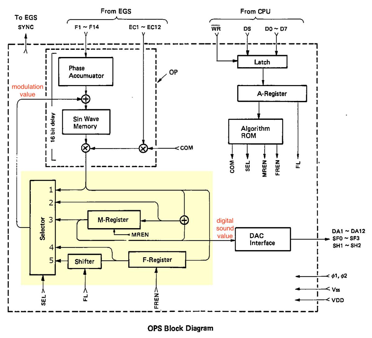
Diagram showing the architecture of the OPS chip, from the DX7/9 Service Manual.

Diagram showing the architecture of the OPS chip, from the DX7/9 Service Manual.

In more detail, the circuitry in the upper left generates the phase values for the 96 oscillators and looks up the values in the sine wave table. In the lower-left, the highlighted block implements the algorithm, producing two outputs. This block contains its own storage: the memory (M) register and feedback (F) register. It generates a modulation value that modulates the index into the sine wave table. It also produces the digital sound value that is the output from the chip. (This highlighted block is the focus of this article.) At the right, the CPU specifies the algorithm number; the algorithm ROM specifies the algorithm by generating control signals COM, SEL, and so forth.

The DX7 has 96 oscillators, which are updated in sequence. The cycle of 96 updates takes place as shown below. In the first clock cycle, computation starts for operator 6 of voice (channel) 1. In the next clock cycles, operator 6 processing starts for voices 2 through 16. Next, operator 5 is processed for the 16 voices, and likewise for operators 4 to 1. At the end of this cycle, all the notes have been updated. Two factors are important here. First, operators are processed "backward", starting at 6 and ending at 1. Second, for a particular voice, there are 16 clock cycles between successive operators. This means that 16 cycles are available to compute each operator.

A complete processing cycle, as shown in the service manual. The overall update rate is 49.096 kHz providing reasonable coverage of the audio spectrum.

A complete processing cycle, as shown in the service manual. The overall update rate is 49.096 kHz providing reasonable coverage of the audio spectrum.

The diagram below provides more detail of highlighted block above, the circuitry that modulates the waveform according to a particular algorithm. The effect of modulation is to perturb the phase angle before lookup in the sine wave table.3 At the bottom right, the signal from operator N+1 enters, and is used to compute the modulation for operator N, exiting at the bottom left.
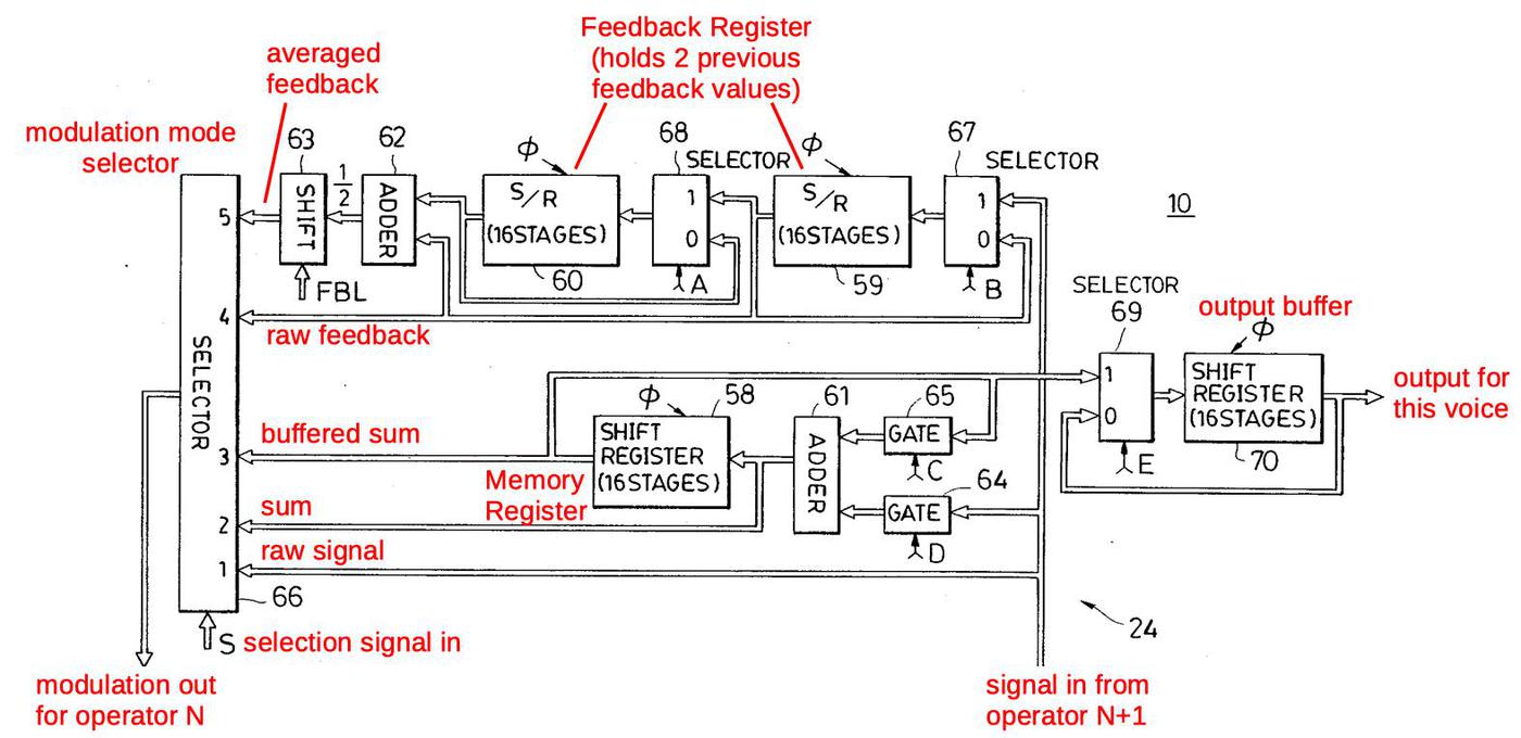
Diagram showing modulation computation, from the patent. Inconveniently, the signal names are inconsistent with the service manual.

Diagram showing modulation computation, from the patent. Inconveniently, the signal names are inconsistent with the service manual.

The key component is the selector at the left, which selects one of the five modulation choices, based on the control signal S or SEL. Starting at the bottom of the selector, SEL=1 selects the unmodified signal from the input operator; this implements the straightforward modulation of an operator by another. Next, SEL=2 uses the value from the adder (61) for modulation. This allows an operator to be modulated by the sum of operators, for instance in algorithm 7. SEL=3 uses the delayed value from the buffer; this is used solely for algorithm 21, where operator 6 modulates operator 4. SEL=4 and SEL=5 use the self-feedback operator for modulation. Because the feedback value is buffered in the circuitry, it is available at any time, unlike other operators. SEL=4 is used to obtain delayed feedback, for instance when operator 6 modulates operator 4 in algorithm 19. (In most cases, feedback is applied immediately, for instance when operator 6 modulates operator 5, and this uses SEL=1.) SEL=5 handles the self-feedback case; the previous two feedback values are averaged to provide stability.4 The SEL=0 case is not shown; it causes no modulation to be selected so the operator is unmodulated.

Several control signals (A, B, C, D, E) also control the circuit. (Confusingly, the patent diagram below uses the names A and B for the feedback register enable (FREN) line. The memory register enable (MREN) lines are called C and D.) Signals A and B have the same value: they select if the feedback buffer continues to hold the previous value or loads a new value. Signals C and D control the buffer/sum shift register. If C is 1 and D is 0, the register holds its previous value. If C is 0 and D is 1, the input signal is loaded into the register. If both C and D are 1, the input signal is added to the previous value. This register can be used to sum two modulation signals, as in algorithm 7. But it is also used to hold and sum the output signals. (As a consequence, an algorithm can't sum modulation signals and outputs at the same time.) Signal E loads the algorithm's final output value into the output buffer (70). Signal E and buffer 70 are implemented separately, so I won't discuss them further.

The algorithm ROM

The algorithms are defined by a ROM with 9-bit entries that hold the selector value (SEL), the control signals MREN and FREN (A,C,D), and the compensation scaling value COM (which I explain later). Each algorithm needs 6 entries in the ROM to select the action for the 6 operators. Thus, the ROM holds 96 9-bit values.

The photo below shows the algorithm ROM. It has 32 columns, one for each algorithm and 9 groups of 6 rows: one group for each output bit. From bottom to top, the outputs are three bits for the selector value SEL, two MREN lines and the FREN line, and three bits for the COM value. The groups of 6 diagonal transistors at the left of the ROM select the entry for the current operator.
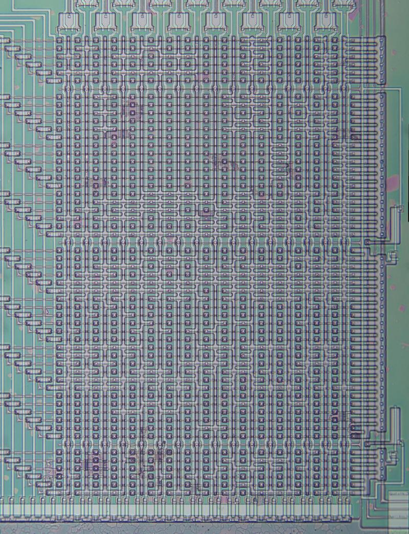
The algorithm ROM. The metal layer has been removed to show the silicon structure underneath that defines the bits.

The algorithm ROM. The metal layer has been removed to show the silicon structure underneath that defines the bits.

The bits are visible in the pattern of the ROM. By examining the ROM closely, I extracted the ROM data. Each entry is formatted as "SEL / A,C,D / COM". (I only show three entries below; the full ROM is in the footnotes.5)

 Operator
Algorithm 654321
11/100/01/000/01/000/10/001/01/010/15/011/0
21/000/01/000/01/000/15/001/01/110/10/011/0
...
81/000/05/001/02/111/10/001/01/010/10/011/0

To see how an algorithm is implemented, consider operator 8, for instance.6

Algorithm 8 has four modulators and two carriers.

Algorithm 8 has four modulators and two carriers.

Processing of an algorithm starts with operator 6's signal value at the output of the operator block and operator 5's modulation is being computed. Table column 6 above shows SEL=1, A,C,D=000. In the modulation circuit (below), SEL=1 selects the raw signal in (i.e. operator 6's value) for modulation. Thus, operator 6 modulates operator 5, the desired behavior for algorithm 8.
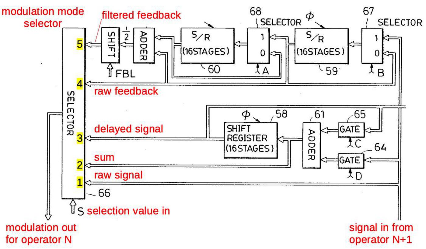
Diagram showing modulation computation.

Diagram showing modulation computation.

Next, (16 cycles later), operator 5's signal is at the output and operator 4's modulation is being computed. Column 5 of the table shows SEL=5, A,C,D=001. SEL=5 selects the filtered feedback register for self-modulation of operator 4. D=1 causes operator 5's value to be loaded into the shift register, in preparation for modulating operator 3.

Next, operator 4's signal is at the output and operator 3's modulation is being computed. Column 4 shows SEL=2 and A,C,D=111. Bits A (and B) are 1 to load the feedback register with operator 4's value, updating the self-feedback for operator 4. Bits C and D cause operator 4 to be added to the previously-stored operator 5 value. SEL=2 selects this sum for operator 3's modulation, so operator 3 is modulated by both operators 4 and 5. COM=1 indicates this operator is one of 2 outputs, so operator 3's value will be divided by 2 as it is computed.

Next, operator 3's signal is at the output and operator 2's modulation is being computed. Looking at the ROM, SEL=0 results in no modulation of operator 2. D=1 loads operator 3's signal into the summing shift register, in preparation for the output.

Next, operator 2's signal is at the output and operator 1's modulation is being computed. SEL=1 causes operator 1 to be modulated by operator 2. C=1 so the summing shift register continues to hold the operator 3 value, to produce the output. As with operator 3, COM=1 so operator 1's value will be divided by 2 when it is computed.

Finally, operator 1's signal is at the output and operator 6's modulation is being computed. SEL=0 indicates no modulation of operator 6. Control signals C and D are 1 so operator 1 is added to the register (which holds operator 3's value), forming the final output.

This process repeats cyclically, interleaved with processing for the 15 other voices. This section illustrates how a complex algorithm is implemented through the modulator circuitry, directed by a few control signals from the ROM. The other algorithms are implemented in similar ways.7

The modulation circuitry

The diagram below shows the circuitry that computes the modulation and output; this functional block is in the center of the chip. The memory register (red) holds 16 values, one for each voice. To its right, the adder (blue) adds to the value in the memory register. The selector (purple), is the heart of the circuit, selecting which value is used for modulation. It is controlled by the selector decoder (orange) at the bottom, which activates a control line based on the 3-bit SEL value. At the far right, the two feedback registers (red) hold the last two feedback values for each of the 16 voices. The feedback adder sums two feedback values to obtain the average. The feedback shifter (yellow) scales the feedback value by a power of 2.
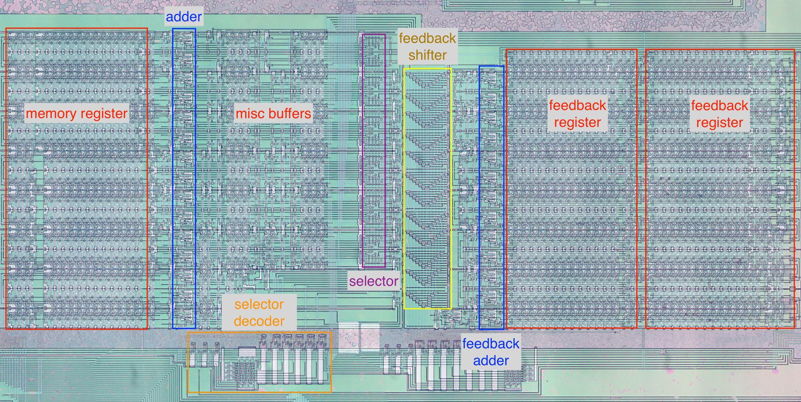
The circuitry that calculates the modulation for the algorithm.

The circuitry that calculates the modulation for the algorithm.

Shift registers

The schematic below shows how one stage of the shift register is implemented. The chip uses a two-phase clock. In the first phase, clock ϕ1 goes high, turning on the first transistor. The input signal goes through the inverter, through the transistor, and the voltage is stored in the capacitor. In the second phase, clock ϕ2 goes high, turning on the second transistor. The value stored in the capacitor goes through the second inverter, through the second transistor, and to the output, where it enters the next shift register stage. Thus, in one clock cycle (ϕ1 and then ϕ2), the input bit is transferred to the output. (The circuit is similar to dynamic RAM in the sense that bits are stored in capacitors. The clock needs to cycle before the charge on the capacitor drains away and data is lost. The inverters amplify and regenerate the bit at each stage.)

Schematic of one stage of the shift register.

Schematic of one stage of the shift register.

The diagram below shows part of the shift register circuitry as it appears on the die. The blue rectangle indicates one shift register stage. The power, ground, and clock wiring is in the metal layer, which was mostly removed in this image. Shift register stages are linked horizontally. Shift registers for separate bits are stacked vertically, with alternating rows mirrored.
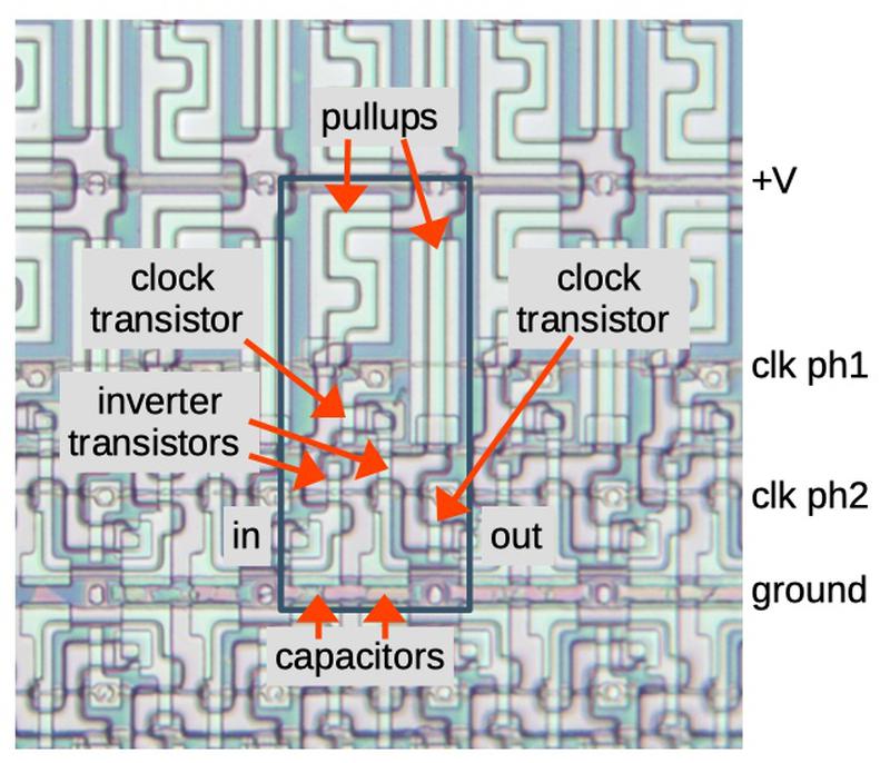
Die photo showing a stage of the shift register.

Die photo showing a stage of the shift register.

The selector

The selector circuit selects one of the five potential multiplexer values, based on the SEL input. The circuit uses five pass transistors (indicated in yellow) that pass one of the 5 inputs to the driver circuit and then the output. (A sixth transistor pulls the output high if none of the inputs is selected; I've labeled this "x".) The diagram below shows one selector in the top half, and a mirror-image selector below; there are 12 selector circuits in total. The circuit is built around the six vertical select lines. One select line is activated to select a particular value. This turns on the corresponding transistors, allowing that input to flow through the transistors. The result goes through another transistor to synchronize it to the clock, and then an inverter/buffer to drive the output line. The outputs go to the sine-wave circuit, where they modulate the input to the lookup table.
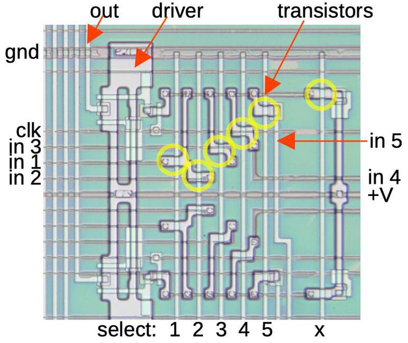
Two stages of the selector.

Two stages of the selector.

The adder

The chip contains multiple adders. Two adders are used in the modulation computation: one to sum operators and one to average the two previous feedback values. The adders are implemented with a standard binary circuit called a full adder. A full adder takes two input bits and a carry-in bit. It adds these bits to generate a sum bit and a carry-out bit. By combining full adders, larger binary numbers can be added.
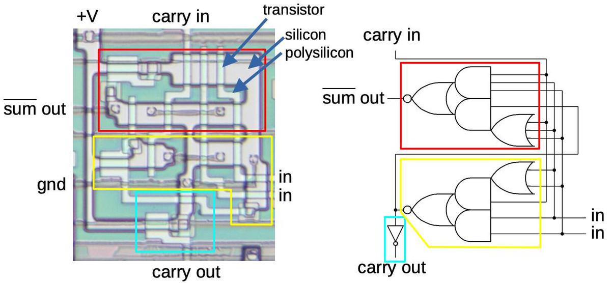
Diagram showing a full adder.

Diagram showing a full adder.

The diagram above shows a full adder stage in the chip. The circuit is built from three relatively complex gates, but if you try the various input combinations, you can see that produces the sum and carry. (Due to the properties of NMOS circuits, it's more efficient to use a small number of complex gates rather than a larger number of simple gates such as NAND gates.)

One problem with binary addition is that it can be relatively slow for carries to propagate through all the stages. (This is the binary equivalent of 99999 + 1.) The solution used in the DX7 is pipelining: an addition operation is split across multiple clock cycles, rather than being completed in a single clock cycle. This reduces the number of carries in one clock cycle. Although a particular addition takes several clock cycles, the adders are kept busy with other additions, so one addition is completed every cycle.

The compensation (COM) computation

In the DX7, different algorithms have different numbers of oscillators in the output, which poses a problem An algorithm with 6 output oscillators (e.g. #32) would be six times as loud as an algorithm with 1 oscillator (e.g. #16), which would be annoying as the user changes the algorithm. To avoid this problem, the chip scales the level of output oscillators accordingly. For instance, the levels of output oscillators in algorithm #32 are scaled by 1/6 to even out the volumes. This factor is called COM (compensation) in the service manual and ADN (addition channel number) in the patent.8 To implement this scaling, the algorithm ROM holds the output count for each operator, minus 1. For example, algorithm #32 has six output oscillators, each one having a COM value of 5 (i.e. 6-1). For algorithm #1, the two output oscillators are 1 and 3: these have a COM value of 1 (i.e. 2-1). Operators that are used for modulation are not scaled, and have a COM value of 0.

Recall that the envelope scaling is accomplished by adding base-2 logarithms. The COM scaling also uses logarithms, which are subtracted to scale down the output level. A small ROM generates 6-bit logarithms for the COM values 1 through 5, corresponding to scale factors 2 through 6. The diagram below shows the COM circuitry, which is in the upper-right corner of the chip. At the left, the decoder and tiny ROM determine the logarithmic scaling factor from the number of inputs. This is added to the logarithmic envelope level that the chip receives from the envelope chip. The result goes through a few shift register stages for timing reasons.
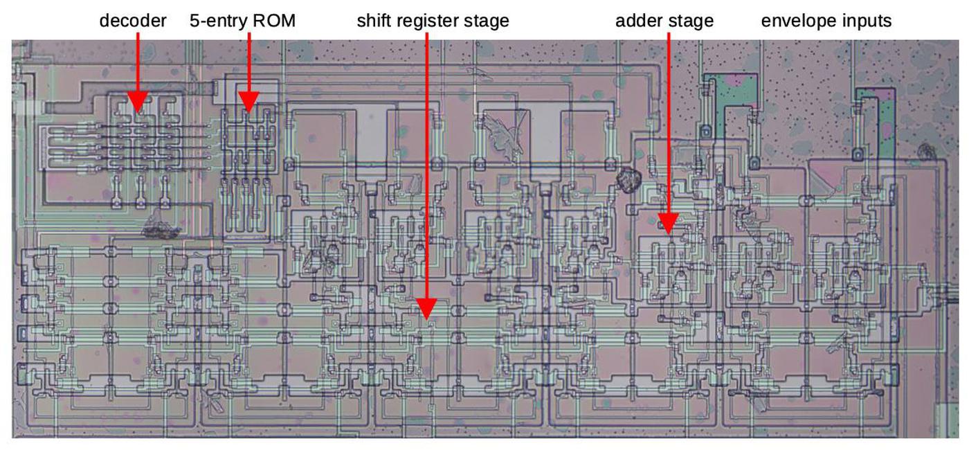
The COM circuitry adds a compensation level to the envelope to compensate for algorithms with multiple outputs.

The COM circuitry adds a compensation level to the envelope to compensate for algorithms with multiple outputs.

Conclusion

The DX7's algorithm implementation circuitry is at the heart of the chip's sound generation. This circuitry is cleverly designed to implement 32 different algorithms at high speed with the limited hardware of the 1980s. The circuitry runs fast enough to process 16 voices sequentially, each with 6 separate oscillators, while producing outputs fast enough to produce audio signals. By taking advantage of the pipelined architecture built around shift registers, the chip processes a different oscillator during each clock cycle, a remarkable throughput. Overall, I'm impressed with the design of this chip. Its cutting-edge design was the key to the DX7's ability to provide dramatic new sounds at a low price. As a result, the DX7 defined the canonical sound of the 1980s and changed the direction of pop music.

I plan to continue investigating the DX7's circuitry, so follow me on Twitter @kenshirriff for updates. I also have an RSS feed. Also see my previous posts on the DX7: DX7 reverse-engineering, the exponential ROM, The log-sine ROM.

Thanks to Jacques Mattheij and Anthony Richardson for providing the chip and discussion.9

Notes and references

  1. Note that the underlying frequency of the oscillator stays the same during modulation, but the phase is changed. Technically the DX7 uses phase modulation (PM) rather than frequency modulation (FM). The two are closely related—phase modulation with a signal is the same as frequency modulation with the derivative of the signal—so the difference is usually ignored. 

  2. Another complication is that the chip is pipelined. It doesn't simply go through 96 clock cycles, updating one operator each cycle. Instead, the computations for an operator are spread across multiple clock cycles. The result is still that one operator calculation is completed per clock, but different parts of the circuitry are working on different operators at any particular time.

    The reason for pipelining is to handle calculations that won't fit into one clock cycle. For instance, the chip adds 22-bit numbers. Propagating a carry through all 22 adder stages would take too long for one clock cycle. Instead, addition takes place in chunks of about 4 bits. The lowest 4 bits are added in one clock cycle, the next bits in the next clock cycle, and so forth. Thus, the propagation delay during one clock cycle is substantially reduced. The circuit still completes one addition per cycle, even though any particular addition takes multiple cycles. 

  3. The diagram below from the patent shows how this is implemented. The modulation is added to the phase angle to create the index into the sine table, yielding the modulated signal. This signal is scaled by the envelope; instead of multiplying, the base-2 logarithms of both values are added. (Ignore ADN for now; I'll discuss it later.) Finally, the logs are converted back to linear values by an exponential ROM and circuit. The result is the modulated and scaled output signal. The steps in this box take exactly 16 clock cycles, which will turn out to be important. As a result, operator N's values enter the box at the same time that operator N+1's values exit the box. (Remember that operators are processed in reverse order: 6 down to 1.)

    Diagram showing the construction of an operator, from the patent.

    Diagram showing the construction of an operator, from the patent.

    I'll summarize the patent's mathematical notation in case anyone reads it. The phase angle, varying with time is ωt. kωt indicates the possible use of a frequency modifier k. The modulation function is f(ωmt), a function of the modulation frequency. The envelope, as a function of t, is A(t) for the amplitude or I(t) for the modulation index; that is, applied to an output operator or a modulating operator respectively. On the diagrams, Φ indicates the clock. 

  4. When an operator provides feedback to itself (usually operator 6), the modulation uses a special path that averages the previous two values. The patent calls this an "anti-hunting" feature. I think this avoids wild oscillations from self-feedback. Suppose you have a situation where a large modulation signal produces a small output and a small modulation signal produces a large output. This would result in the signal oscillating between small and large every clock cycle, which would be unpleasant. Averaging the previous two values is essentially a low-pass filter and would prevent these wild oscillations. Also note that the self-feedback path allows the feedback level to be controlled by the FBL signal. This shifts the feedback signal, dividing it by a power of 2. 

  5. The full algorithm ROM contents are below. The format is "SEL/ FREN MREN / COM value". Note that algorithm numbers are 1 to 32, while the ROM's binary addresses are 0 to 31.

     Operator
    Algorithm 654321
    11/100/01/000/01/000/10/001/01/010/15/011/0
    21/000/01/000/01/000/15/001/01/110/10/011/0
    31/100/01/000/10/001/01/010/01/010/15/011/0
    41/000/01/000/10/101/01/010/01/010/15/011/0
    51/100/20/001/01/010/20/011/01/010/25/011/0
    61/000/20/101/01/010/20/011/01/010/25/011/0
    71/100/00/001/02/011/10/001/01/010/15/011/0
    81/000/05/001/02/111/10/001/01/010/10/011/0
    91/000/00/001/02/011/15/001/01/110/10/011/0
    100/001/02/011/15/001/01/110/01/010/10/011/0
    110/101/02/011/10/001/01/010/01/010/15/011/0
    120/001/00/011/02/011/15/001/01/110/10/011/0
    130/101/00/011/02/011/10/001/01/010/15/011/0
    140/101/02/011/01/000/10/001/01/010/15/011/0
    150/001/02/011/01/000/15/001/01/110/10/011/0
    161/100/00/001/01/010/00/011/02/011/05/001/0
    171/000/00/001/01/010/05/011/02/111/00/001/0
    181/000/01/000/05/001/00/111/02/011/00/001/0
    191/100/24/001/20/011/01/010/01/010/25/011/0
    200/001/02/011/25/001/01/110/24/011/20/011/0
    211/001/33/001/35/011/01/110/34/011/30/011/0
    221/100/34/001/34/011/30/011/01/010/35/011/0
    231/100/34/001/30/011/01/010/30/011/35/011/0
    241/100/44/001/44/011/40/011/40/011/45/011/0
    251/100/44/001/40/011/40/011/40/011/45/011/0
    260/101/02/011/20/001/01/010/20/011/25/011/0
    270/001/02/011/25/001/01/110/20/011/20/011/0
    285/001/01/110/01/010/20/011/01/010/20/011/2
    291/100/30/001/01/010/30/011/30/011/35/011/0
    305/001/01/110/01/010/30/011/30/011/30/011/3
    311/100/40/001/40/011/40/011/40/011/45/011/0
    320/101/50/011/50/011/50/011/50/011/55/011/5
     

  6. The DX7/9 service manual explains the steps of algorithms 1 and 21 in detail. 

  7. Note that the algorithms are carefully designed with operator 6 on top and 1 on the bottom, so operators are modulated only by operators with a higher number. This is due to the implementation of the modulation circuitry which processes operators starting with 6 and ending with 1. The 32 algorithms make it look like almost anything is possible, but the hardware imposes several constraints that limit the possibilities. For instance, there is only one sum/delay register so you can't sum modulators and the output at the same time. You can't delay a non-feedback operator after an output takes place; for instance, algorithm 11 has 6 delayed to modulate 3, but only because there haven't been any outputs at that point. An algorithm can only have one self-feedback loop. 

  8. The logarithmic COM values are:

    COMbinary valuevalue
    000.000log2(1)
    101.000log2(2)
    201.101≈log2(3)
    310.000log2(4)
    410.011≈log2(5)
    510.101≈log2(6)

    Since the computation is done with logarithms, the circuit subtracts these values (or equivalently adds the complement). This is equivalent to dividing by the number of outputs or multiplying by the reciprocal. Note that the COM input is one less than the number of outputs. Entry 0 is not explicitly stored in the ROM but results by default. If the result of the subtraction is negative, gates clamp the envelope at 0. 

  9. For more information on the DX7 internals, see DX7 Technical Analysis, DX7 Hardware, OPLx decapsulated, and the video Emulating the DX7 the hard way

Yamaha DX7 reverse-engineering, part III: Inside the log-sine ROM

The Yamaha DX7 digital synthesizer (1983) was the classic synthesizer for 1980s pop music. It used two custom digital chips to generate sounds with FM synthesis. In this blog post, I examine the log-sine ROM that digitally produces sine waves inside one of these chips. (This blog post jumps into the details; unless you care about the sine values specifically, my previous DX7 reverse-engineering article is probably more interesting.)

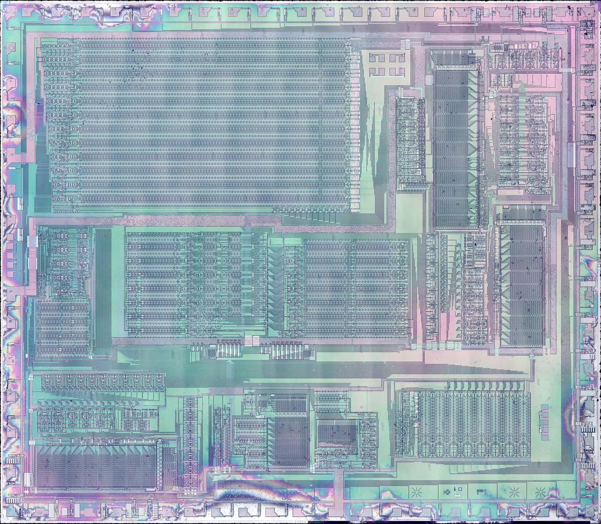
I created the high-resolution die photo below by compositing over a hundred microscope photos. I removed the metal layer from the chip with acid to reveal the silicon and polysilicon wiring underneath. You can see the structure of the functional blocks and the connections between them. The colors are due to variations in thickness of the oxide layer, causing thin-film interference. With the metal layer removed, I could read out the bits from the ROM, reverse-engineer the circuitry, and determine the exact values used for sine-wave generation.

Die photo of the DX7's YM21280 Operator chip.  Click this photo (or any other) for a magnified version.

Die photo of the DX7's YM21280 Operator chip. Click this photo (or any other) for a magnified version.

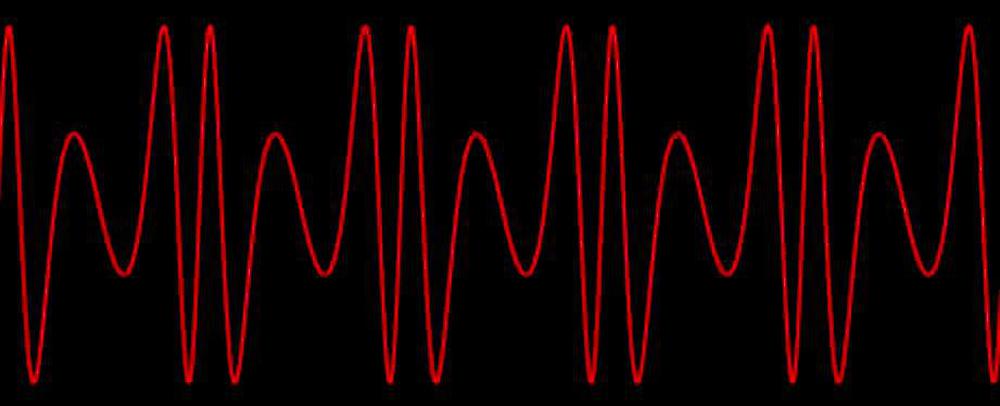
Instead of the analog oscillators and filters of an analog synthesizer, the DX7 generates sounds digitally, using a technique called FM synthesis. The idea is that you start with a sine wave (the carrier signal) and perturb it with another signal (the modulating signal). The modulating signal changes the phase (and thus the frequency) of the carrier, creating complex harmonic structures like the waveform below. These signals are represented as digital values throughout the system; a digital-to-analog converter (DAC) turns the digital representation into an analog voltage for the synthesizer's output.

An example of a complex waveform created by FM synthesis.  (I made a tool that lets you experiment with FM synthesis.)

An example of a complex waveform created by FM synthesis. (I made a tool that lets you experiment with FM synthesis.)

The digital implementation of frequency modulation uses a lookup table that holds a digitized sine wave. By stepping an index through the table at a specific rate, you can produce a sine wave of a fixed frequency. By perturbing this index with another signal, you can produce a modulated sine wave like the one below. The DX7 implements this with a sine-wave table in ROM, an increment value that controls the frequency, and an adder that adds the increment to the table index (i.e. the phase angle) each time step. This ROM is the subject of this blog post.

The amplitude of the sine wave is controlled by an envelope, varying over time; multiplying the sine wave by the envelope level yields the output. However, fast multiplication required too much hardware in the 1980s, so the DX7 uses a mathematical shortcut: adding logarithms is equivalent to multiplying the values. The obvious problem is that computing logarithms is harder than multiplying, but the trick is to store the (negated) logarithm of the sine wave in the lookup table (below) instead of the sine wave. This provides the logarithm for free. (The other issue is that you need to perform an exponential to get the final result. I described the exponential ROM and circuit in my previous DX7 article).

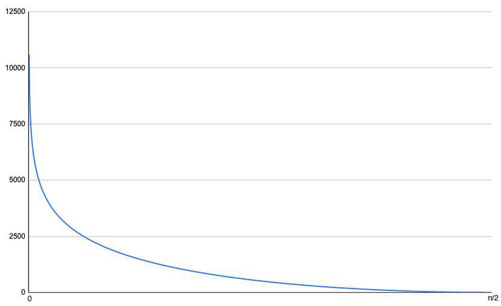
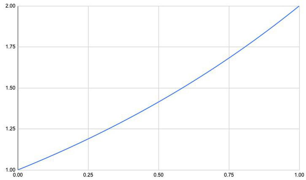
This graph shows the log-sine function over one quarter of the wave, as a 14-bit value. It's not recognizable as a sine function, but will turn into a sine wave after exponentiation.

This graph shows the log-sine function over one quarter of the wave, as a 14-bit value. It's not recognizable as a sine function, but will turn into a sine wave after exponentiation.

The block diagram below shows the structure of the log-sine circuit, computing a 14-bit value from a 12-bit input. The circuitry is somewhat complex to fit a fast, high-accuracy calculation into a small space on the die. The implementation takes advantage of the symmetry of the sine wave so only a quarter-wave needs to be stored. The top bit is used as the sign bit, which inverts the output elsewhere to obtain the negative half of the sine wave. (This also avoids the problem of taking the log of a negative value.) The second bit implements the mirror symmetry of each sine-wave peak by inverting the bits for the second half of the peak.

Block diagram of the sine circuit. Input bits are indicated in green.

Block diagram of the sine circuit. Input bits are indicated in green.

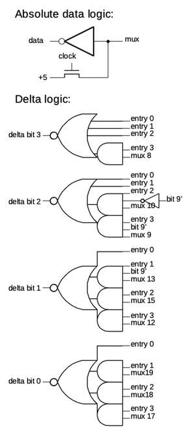
The ROM and associated logic take a 10-bit input address representing a quarter of the sine wave (angles 0 through π/2). A technique called delta encoding is used to reduce the size of the ROM. The idea of delta encoding is that if values change slowly, the difference between two values is considerably smaller than the value itself.1 Specifically, only every fourth value is explicitly stored in the ROM; this value is called an "absolute" value.3 The next three values are stored as deltas: the difference between the value and the previous absolute value.2 An adder circuit adds the absolute value to the difference value, yielding the desired log-sin value.

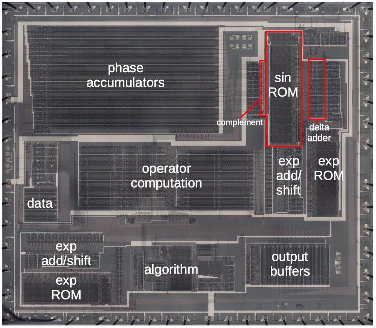
The diagram below labels the main functional blocks of the chip. In this article, I focus on the sine circuit, highlighted in red, but I'll summarize the other blocks. The 96 phase accumulators, implemented with shift registers, are the largest block of the chip. They hold the current table index for each of the DX7's 96 oscillators. The exponential function is implemented by two identical ROMs and associated addition/shifter circuitry. Other major blocks apply the envelope, hold configuration data, compute the operators that combine oscillators, define different operator algorithms, and buffer the output values.

Die with the major functional blocks labeled. This photo shows the metal layer of the chip. (Click for a larger version.)

Die with the major functional blocks labeled. This photo shows the metal layer of the chip. (Click for a larger version.)

The ROM

The photo below shows the log-sin ROM. The ROM itself consists of a grid of transistors. At the top, decoder circuits select signal lines based on the address bits. At the right, the diagonal circuits are multiplexers, selecting particular rows of the ROM. To the right of the multiplexers, logic circuits select the delta values. I won't explain these circuits in detail since I discussed the similar circuits for the exponential ROMs in my previous article.

High-resolution image of the sine ROM. Click this image (or any other) for an enlarged image.)

High-resolution image of the sine ROM. Click this image (or any other) for an enlarged image.)

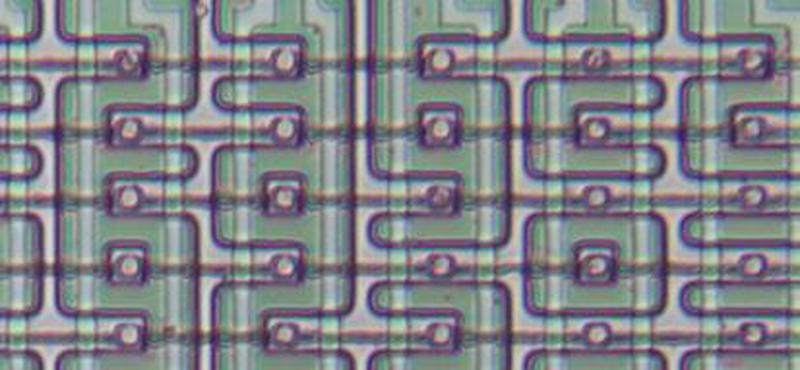
By examining the ROM closely, you can see the individual transistors that store bits. A transistor represents a 1, and the lack of a transistor represents a 0. Thus, the data in the ROM is created by the pattern of how the silicon is doped. I was able to read out the ROM data visually by looking at this pattern.

Closeup of the ROM.

Closeup of the ROM.

The delta representation and the adder

The ROM itself produces 43 output bits, 13 bits for the "absolute" value and 30 bits for the three delta values. Some logic circuitry expands the ROM's 30 bits into three deltas of 12 bits (and a zero delta for the absolute value), taking advantage of some structure in the deltas. This circuitry is just to the right of the ROM and is implemented with AND-OR-INVERT gates. These gates implement 4-to-1 multiplexers, selecting the appropriate delta value based on the 2 lowest input bits.

Next, the adder circuit to the right of the ROM adds the 13-bit absolute value and the 12-bit delta value to generate the final 14-bit value. One interesting feature of the adder is it is pipelined to minimize the delay from carry propagation. I discussed the adder implementation in my previous article so I won't go into details here. The adder is immediately followed by a second adder that adds the envelope value to scale the signal level, taking advantage of the logarithmic representation.

Overall, the log-sine circuit generates 1024 14-bit values. Stored directly, this would take over 14 kilobits, but the ROM is only 5344 bits. The delta representation and ROM compression reduce the ROM size by almost 63%, important for a chip built in the 1980s when transistors were precious. By itself, the delta representation doesn't save much space: a 12-bit delta instead of a 14-bit value. But the ROM's implementation makes the deltas efficient: if a 32-bit row in the ROM is all zeroes, the row can be omitted entirely and the output defaults to 0. For the flat parts of the function, the high-order bits of the deltas are mostly zero, so much of the ROM can be omitted.

Conclusion

The DX7 generates its waveforms from a digital sine wave, so producing a high-accuracy value rapidly is key to the synthesizer's performance. By examining the ROM and associated circuitry, I could obtain the exact values that the DX7 uses for the log-sine function. The ROM provides one quarter of the sine wave and the other quarters are formed by symmetry. For a 10-bit input value n, the corresponding angle is ω = (n + .5)/1024×π/24 and output value y is -log2(sin(ω)), represented as the integer round(y×1024).5

The DX7's OPS chip comes in a 64-pin ceramic package with staggered pins. This is known as a Quad Inline Package (QIP). Photo courtesy of Jacques Mattheij.

The DX7's OPS chip comes in a 64-pin ceramic package with staggered pins. This is known as a Quad Inline Package (QIP). Photo courtesy of Jacques Mattheij.

I plan to continue investigating the DX7's circuitry, so follow me on Twitter @kenshirriff for updates. I also have an RSS feed.

Thanks to Jacques Mattheij and Anthony Richardson for providing the chip and discussion.6

Notes and references
  1. A different chip, the Yamaha YMF262 (1988) was used in computer sound cards such as the Sound Blaster 16. (This chip is also known as OPL3 for FM Operator Type-L.) It uses FM synthesis, but is stripped down compared to the DX-7. The chip was reverse-engineered by Matthew Gambrell and Olli Niemitalo who decapsulated the chip and read out the ROM contents.

    The OPL3 log-sine ROM is similar to the DX7's in some ways, but is lower resolution. The OPL3 chip is 256 samples long, rather than 1024, and holds 8-bit values, rather than 13-bit values. Both chips use delta encoding, but the OPL3 has one delta-encoded value for each absolute value, while the DX7 has three delta-encoded values. 

  2. To be precise, the three delta values are stored before the absolute value in the ROM. That is, entries 3, 7, 11, ... are absolute, instead of 0, 4, 8, ..., the expected locations. I think this is because the log-sin function is decreasing, so if you want to add the deltas (instead of subtracting), the absolute value needs to be the last of the group, not the first. 

  3. The absolute value in delta encoding is the full, explicit value. It's unrelated to the absolute value function |x|. 

  4. Note that the input to the ROM is incremented by half a bit. This avoids duplication of the 0 value of the waveform when the quarter-wave is mirrored. It also avoids computation of the undefined value log(0). 

  5. The value is rounded to an integer by computing int(y×1024 + .5002). The constant .5002 rounds the value up, with just a tiny bit more that affects a single entry. I'm not sure why the rounding is not exact; perhaps Yamaha used a lower-precision sine or logarithm, which was just enough to change one bit. (Note that the value .0002 is somewhat arbitrary; a slightly larger or smaller number will yield the same result.) 

  6. For more information on the DX7 internals, see DX7 Technical Analysis, DX7 Hardware, OPLx decapsulated, and my previous DX7 articles Reverse-engineering the Yamaha DX7 synthesizer's sound chip from die photos and The Yamaha DX7's exponential circuit

The Yamaha DX7 synthesizer's clever exponential circuit, reverse-engineered

The Yamaha DX7 digital synthesizer was released in 1983 and became extremely popular, defining the sound of 1980s pop music. Because microprocessors weren't fast enough in the early 1980s, the DX7 used two custom digital chips: the EGS "envelope" chip generated frequency and envelope data, which it fed to the OPS "operator" chip that generated the sound waveforms. A key part of the OPS chip is an exponential circuit, which is used for frequency calculation and envelope application. In this blog post, I examine this circuit—implemented by a ROM, shifter, and other circuitry—in detail and extract the ROM's data.

I created the high-resolution die photo below by compositing over a hundred microscope photos. Around the edges, you can see the 64 bond wires attached to pads; these connect the silicon die to the chip's 64 pins. The chip has one layer of metal, visible as the whitish lines on top. (Power and ground are the thick metal lines.) Underneath the metal, the polysilicon wiring layer appears reddish or greenish. Finally, the underlying silicon is grayish. I discussed the chip as a whole in my previous DX7 article; now I will focus on the exponential circuit.

Die photo of the DX7's YM21280 Operator chip.  Click this photo (or any other) for a magnified version.

Die photo of the DX7's YM21280 Operator chip. Click this photo (or any other) for a magnified version.

The DX7 was the first commercially successful digital synthesizer. Instead of the analog oscillators and filters of an analog synthesizer, the DX7 generates sounds digitally, using a technique called FM synthesis. The idea is that you start with a sine wave (the carrier signal) and perturb it with another signal (the modulating signal). The modulating signal changes the phase (and thus the frequency) of the carrier, creating complex harmonic structures. These signals are represented as digital values throughout the system; a digital-to-analog converter (DAC) turns the digital representation into an analog voltage for the synthesizer's output.

The digital implementation of frequency modulation uses a lookup table that holds a digitized sine wave. By stepping an index through the table at a specific rate, you can produce a sine wave of a fixed frequency. By perturbing this index with another signal, you can produce a modulated sine wave. The DX7 implements this with a sine-wave table in ROM, an increment value that controls the frequency, and an adder that adds the increment to the table index (i.e. the phase angle) each time step. The DX7 has 96 oscillators, so it keeps track of 96 separate phase angles; these are stored in the phase accumulators. The frequency modulation is implemented by operator circuitry, which allows oscillators to perturb other oscillators. (This is a very brief overview of FM synthesis; see my previous DX7 reverse-engineering article for more details.)

Logarithms and exponentials

In hardware, multiplication is much slower than addition, especially with 1980s-era technology. The solution in the DX7 is to represent values as base-2 logarithms because adding logarithms is equivalent to multiplying the values. By applying 2x to the sum, the logarithmic value can be converted back to a linear value.

The first role for logarithms is in the frequency input to the chip: the phase increment value supplied to the chip is logarithmic. The motivation is that note frequencies are related exponentially: for instance, going up one octave doubles the frequency. By using logarithms, note computations can be done with addition.

Second, each oscillator has an associated envelope, which changes the output level according to a time-varying curve.1 To multiply the signal by the envelope level, the sine wave signal and the envelope are both represented logarithmically. Thus, the multiplication is replaced by addition. (The logarithm of the sine-wave signal is conveniently obtained by storing log2(sin(x)) in the waveform ROM instead of sin(x), so the logarithm is obtained "for free".)

The block diagram below shows the structure of the exponential circuit that converts the logarithmic value to a linear value by computing 2x. The exponential circuitry is somewhat complex to fit a fast, high-accuracy exponential calculation into a small space on the die. The circuit takes a 14-bit input value that consists of a 4-bit integer part and 10 fractional bits, so it computes 2x for 0≤x<16.2 The circuit uses a ROM lookup and a shift to rapidly compute the value.

Block diagram of the exponentiation circuit. Input bits are indicated in green.

Block diagram of the exponentiation circuit. Input bits are indicated in green.

The ROM takes a 10-bit input address (0 through 1023) representing x values 0 through 1023/1024. A technique called delta encoding is used to reduce the size of the ROM. The idea of delta encoding is that if values change slowly, the difference between two values is considerably smaller than the value itself.3 Specifically, only every fourth value is explicitly stored in the ROM; this value is called an "absolute" value.7 The next three values are stored as the deltas, difference between the value and the previous absolute value. The deltas fit into 4 bits4, a considerable saving over the 11-bit absolute values. An adder circuit adds the absolute value to the difference value, yielding the desired exponential value.

The final step in the exponential circuity is to perform a binary shift on the value from the ROM. Shifting by the number of bits in the integer part of the input results in the final exponential value.6 Prior to shifting, a leading 1 is added to the ROM's value so this bit doesn't take up space in the ROM.5 The chip has two exponentiation circuits: one for computing the frequency and one for computing the signal (the sine and envelope path). Most of the circuitry is identical between the two, but the frequency exponent produces 22 bits of output, while the signal exponent has just 14 bits of output.

A closer look at the die

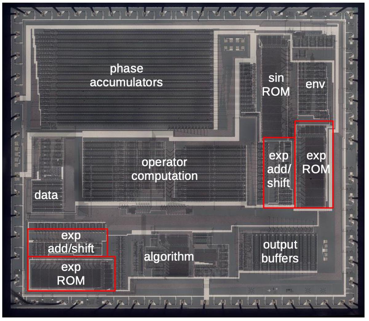
The diagram below labels the pins and the main functional blocks of the chip. In this article, I focus on the two exponential circuits, highlighted in red, but I'll summarize the other blocks. The 96 phase accumulators, implemented with shift registers, are the largest block of the chip. ROMs hold the sine wave function and the exponential function. (There are two identical exponential ROMs, with associated adder and shifter circuitry.) Other major blocks apply the envelope, hold configuration data, compute the operators that combine oscillators, define different operator algorithms, and buffer the output values.

Die with the major functional blocks labeled. This photo shows the metal layer of the chip. (Click for a larger version.)

Die with the major functional blocks labeled. This photo shows the metal layer of the chip. (Click for a larger version.)

Transistors

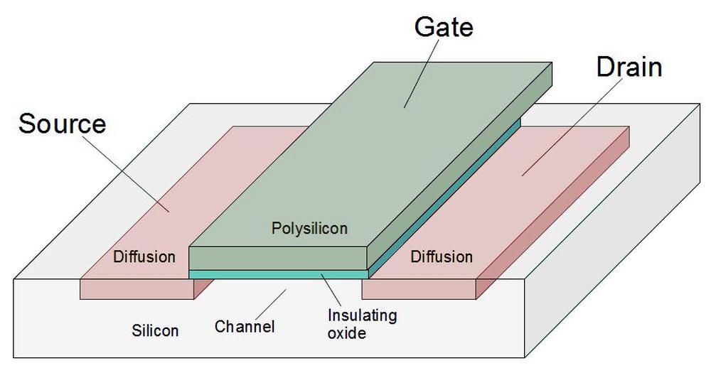
To explain the die photos, I'll first show how a transistor (below) is constructed in an NMOS integrated circuit. Regions of the silicon are doped with impurities to create diffusion regions with desired properties. The transistor can be viewed as a switch, allowing current to flow between two diffusion regions called the source and drain. The transistor is controlled by the gate, made of a special type of silicon called polysilicon. A high voltage on the gate lets current flow between the source and drain, while a low voltage blocks current flow. These tiny transistors are combined to form logic gates and other circuits.

Structure of an NMOS transistor (MOSFET) as implemented in an integrated circuit.

Structure of an NMOS transistor (MOSFET) as implemented in an integrated circuit.

To make the transistors more visible, I removed the metal layer from the chip, resulting in the high-resolution die photo below. (The colors are due to variations in the thickness of the oxide layer due to my etching process.)

Die photo of the DX7's YM21280 Operator chip with the metal layer removed.  Click this photo (or any other) for a magnified version.

Die photo of the DX7's YM21280 Operator chip with the metal layer removed. Click this photo (or any other) for a magnified version.

The ROM

The diagram below shows one of the exponential ROMs. The ROM is constructed from a grid of transistors: 128 rows by 32 columns.8 At each grid point, a transistor can be present, representing a 1 bit; or a transistor can be absent, representing a 0 bit.9

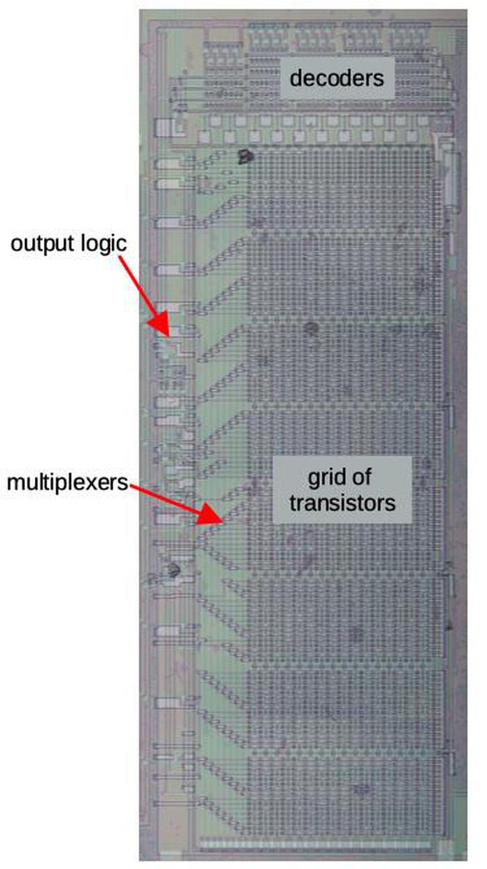
At the top, decoders activate one of the 32 vertical select lines in the ROM, based on five bits of the address. The ROM is arranged into groups of 8 rows (or fewer, depending on compression). A multiplexer selects one bit of each group, based on three bits of the address. This produces a 20-bit output. Finally, the output logic produces the desired delta value, based on the address. The result is the 11-bit absolute value and a 4-bit delta value.

The ROM with the main components labeled.

The ROM with the main components labeled.

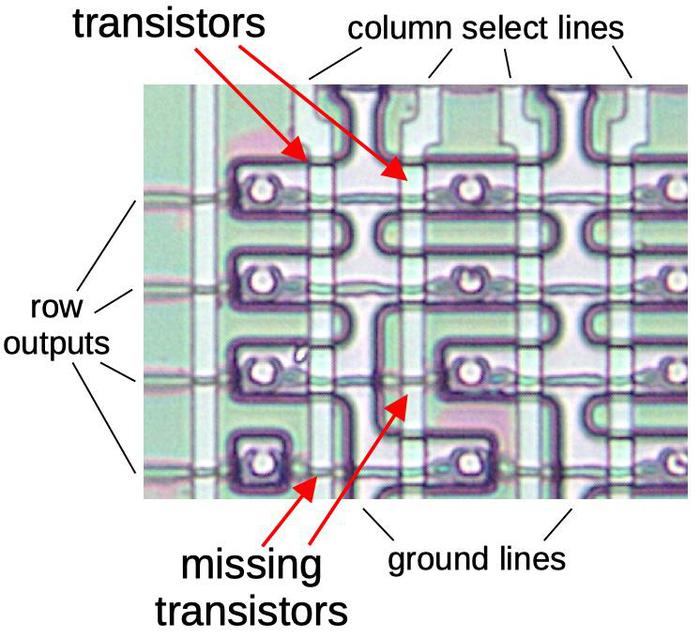
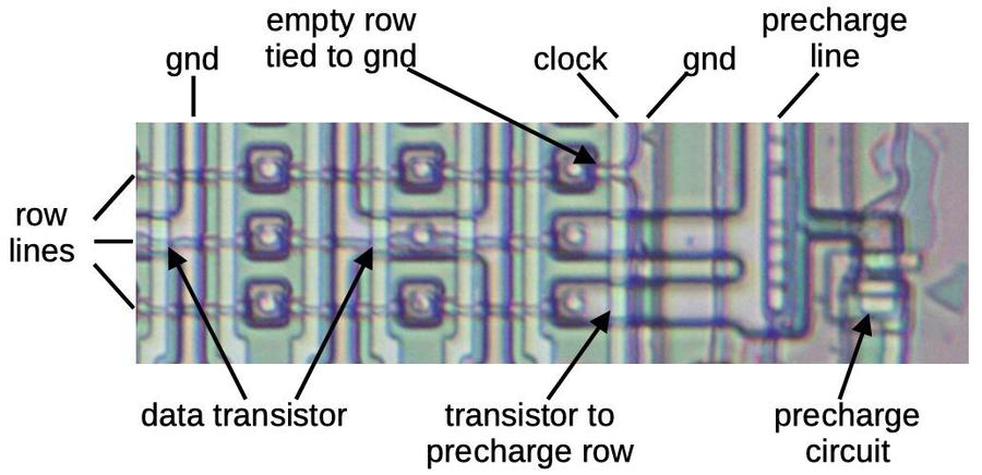
Zooming in on the ROM shows the individual transistors. The large pale regions are the doped silicon, forming transistor sources and drains. The polysilicon select lines are vertical. A transistor is formed when a polysilicon line crosses a doped silicon region. The indicated silicon regions are connected to ground, pulling one side of each transistor low. The circles are connections called vias between the silicon and the metal lines above. (The metal lines have been removed but the wavy horizontal lines show where the metal was.)

Closeup of a 4×4 section of the ROM, showing its construction.

Closeup of a 4×4 section of the ROM, showing its construction.

Each bit is stored in the ROM by the presence or absence of a transistor at a grid position. (During manufacturing, the silicon doping pattern controls whether or not a transistor exists.) When one of the 32 select lines is activated, all the transistors in that column will turn on, pulling the corresponding output lines low. But if a transistor is missing, the corresponding output line will remain high. Thus, a value is read from the ROM by activating a select line, reading that ROM value onto the output lines. By looking at the silicon pattern in the ROM, I determined the sequence of 1's and 0's stored in the ROM, 4 kilobits in total.

The multiplexer

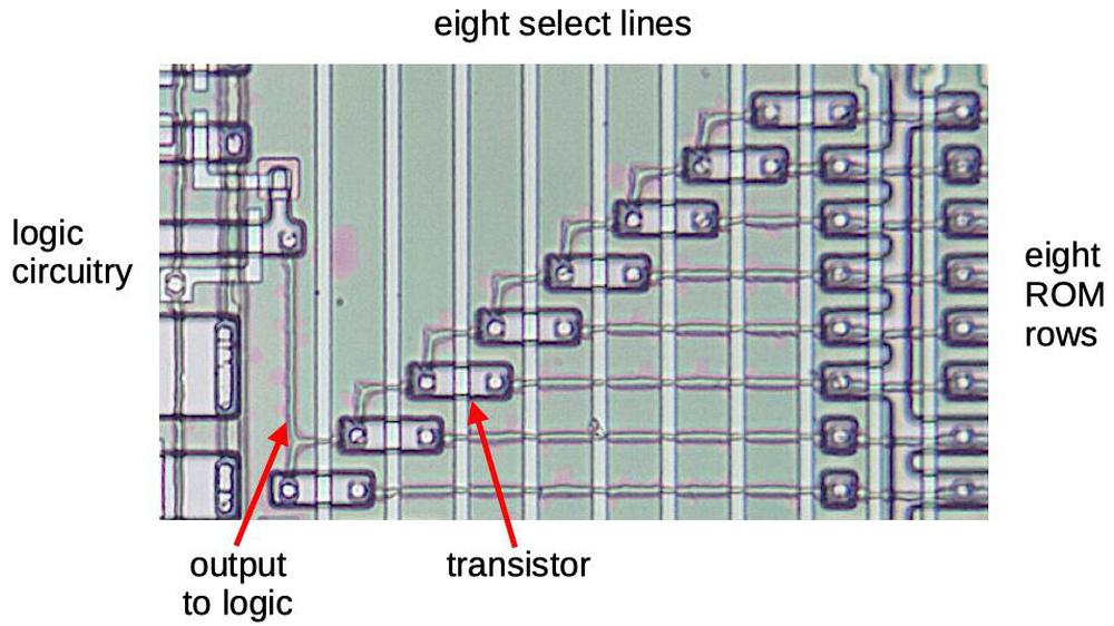
The ROM has 256 entries of 20 bits, before the delta processing is applied. To make the layout more efficient, the ROM stores bits in groups of 8, (conceptually) organized as 8 rows of 32 entries (columns) for each output bit. Each output bit has a multiplexer that selects one of the 8 bits in the group, based on 3 more address lines that control the 8 multiplexer select lines.

A multiplexer in the ROM.

A multiplexer in the ROM.

Each multiplexer (above) is implemented by 8 pass transistors. One transistor is activated, letting that row's bit through, while the unselected rows are blocked. The output of the multiplexer goes to the logic circuitry on the left.

Looking at the die photo closely shows that some of the multiplexers don't have all eight rows. This is a key optimization to reduce the ROM size. If all the bits in a row are 0, the row can be eliminated from the ROM entirely.10

The delta logic and the adder

The ROM produces 20 output bits, 11 bits for the "absolute" value and 9 bits for the three delta values. Some logic circuitry expands the ROM's 9 bits into three deltas of four bits, taking advantage of some structure in the deltas.11

To obtain the 2x-1 value, the 11-bit absolute value and the 4-bit delta must be added. This is accomplished by an adder circuit to the left of the ROM. One interesting feature of the adder is it is pipelined to minimize the delay from carry propagation. I discussed the adder in my previous article so I won't go into details here.

The bit shifter

The final building block that I'll discuss is the bit shifter, which implements the integer part of the exponential calculation. It shifts the value to the left by 0 to 15 bits, which is equivalent to multiplying by a power of 2. The shifter is built in two layers: the bottom layer shifts by 0, 1, 2, or 3 positions. The upper layer shifts by 0, 4, 8, or 12 positions. The combination of the two layers permits any shift between 0 and 15 bit positions. Wiring between the two layers distributes the outputs from the first layer to the second layer. Each output goes to four inputs, each spaced 4 bits apart to provide the larger shift.

The shifter circuit.

The shifter circuit.

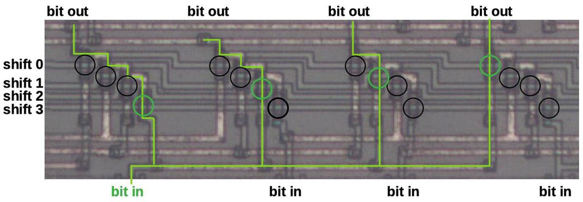
The diagram below shows part of the shifter that shifts by 0, 1, 2, or 3 positions, controlled by the horizontal lines. The shifter is built from multiplexers, similar to those in the ROM, that select one of four inputs. I've highlighted one of the bits in green. If the "shift 0" line is activated, the rightmost green transistor (circled) will turn on and the green input bit will exit from the rightmost output. Likewise, if the "shift 1" line is activated, the second green transistor will turn on and the green bit will exit shifted one position to the left. The "shift 2" and "shift 3" lines will cause the green bit to be shifted two or three positions to the left. The remaining transistors (circled in black) act in the same manner to shift the other bits. The result is that all the bits will be shifted by shifted 0, 1, 2, or 3 positions. The second shifter is similar, except the input lines go to multiplexers that are four positions apart.

Detail of the shifter circuit.

Detail of the shifter circuit.

Conclusion

Computing exponents is a key part of the DX7's sound synthesis. The chip needs to compute exponents very quickly, faster than an algorithm such as CORDIC could operate, but a straightforward ROM would have been much too large. The chip solves this dilemma by using delta encoding, ROM compression, and a shifter circuit. These techniques reduced the ROM size by almost 64%.12 By examining the circuitry closely, I have reverse-engineered the exact values that are generated. DX7 emulators may be able to achieve more accuracy by using these values.

The DX7's OPS chip comes in a 64-pin ceramic package with staggered pins. This is known as a Quad Inline Package (QIP).

The DX7's OPS chip comes in a 64-pin ceramic package with staggered pins. This is known as a Quad Inline Package (QIP).

The next step is to reverse-engineer the chip's sine wave ROM, which implements the log-sin function. That ROM uses many of the same techniques as the exponential ROM, but stores the deltas differently, for instance. I announce my latest blog posts on Twitter, so follow me @kenshirriff for updates. I also have an RSS feed. If you're interested in ROM data, I also wrote about extracting constants from the 8087 floating point chip.

Thanks to Jacques Mattheij and Anthony Richardson for providing the chip and discussion.14

Notes and references
  1. For an output signal, the envelope gives the note a more realistic sound; a typical sound has a sharp attack when it is first played, and then the volume decays. The level is sustained until the key is released, and then dies off quickly. However, the DX7 also applies envelopes to the modulating signals, allowing the timbre of the note to change over time. 

  2. The exact values of the exponentiation circuit are given as follows. Suppose the 14-bit input value is int.frac, where int is the 4-bit integer part and frac is the 10-bit fractional part. The 12-bit output value from the ROM, after the delta adder and appending a leading 1 bit, is exactly given by round(2frac×2048). The shifter applies a left shift of 0 to 15 bits and then the result is truncated to 22 or 14 bits, for the frequency and signal exponentiation respectively. The final results are
    round(2frac× 2048) << int >> 5, and
    round(2frac× 2048) << int >> 13, respectively
    (where << and >> are the bit shift operators).

    In both cases, the fixed 1 is in the leftmost position of the output when the input has maximum integer portion (i.e. 15). (This is necessary since otherwise the value would either get truncated, or the leftmost bit would be unused.) However, with input integer portion of 0, the frequency circuit still has 7 bits of output, while the envelope circuit produces a value of 0 (since all the bits are lost in shifting). 

  3. A different chip, the Yamaha YMF262 was used in computer sound cards such as the Sound Blaster 16. (This chip is also known as OPL3 for FM Operator Type-L.) It uses FM synthesis, but is stripped down compared to the DX-7. The chip was reverse-engineered by Matthew Gambrell and Olli Niemitalo who decapsulated the chip and read out the ROM contents.

    The OPL3 exponential ROM is similar to the DX7's in some ways, but is also very different. The OPL3 chip is 256 samples long, rather than 1024, and holds 10-bit values, rather than 12-bit values. Both chips use delta encoding, but the OPL3 has one delta-encoded value for each absolute value, while the DX7 has three delta-encoded values. 

  4. The graph below shows the exponential function 2x over the fractional range. The difference between successive elements is fairly small, so a 4-bit delta value is sufficient. Storing a 4-bit difference instead of an 11-bit absolute value achieves a large space saving.

    Graph of 2x over the fractional range.

    Graph of 2x over the fractional range.

    Since the exponential function is convex, the largest delta in the exponential table is at the right, specifically (21023/1024-21020/1024)×2048 ≈ 8.3. The delta almost fits into three bits, but four bits are required. 

  5. The ROM stores 2x-1 rather than 2x, since all the values have a leading one. Specifically, for 0≤x<1, 1≤2x<2. Adding 1 to the ROM's output instead of explicitly storing it in the ROM reduces the ROM's size. 

  6. Mathematically, if the input value is split into integer and fractional parts: int+frac, then 2int+frac = 2int×2frac. Multiplying by 2int is the same as performing a binary shift int bits to the left. 

  7. The absolute value in delta encoding is the full, explicit value. It's unrelated to the absolute value function |x|. 

  8. The two exponential ROMs on the chip are identical, except one is horizontal and one is vertical. This makes referring to rows and columns a bit ambiguous; hopefully it all makes sense. 

  9. Whether a transistor in the ROM represents a 1 or a 0 is somewhat arbitrary, since the signal gets inverted several times before use. A transistor will cause that line of the ROM to be pulled low, so at the fundamental level a transistor represents a 0. However, in the exponential ROM, this value is immediately inverted, so a transistor represents a 1 bit in the final result. 

  10. The ROM operates in two phases, controlled by the clock. In the first phase, the rows and the multiplexers are all pulled high. In the second phase, the desired ROM column is activated. If there are transistors, they will pull the rows low. Through the selected multiplexer transistor, this will pull the multiplexer low. The multiplexer output is then inverted, so a position with a transistor represents a logical 1 and the absence of a transistor represents a logical 0. With this circuit, if a row and multiplexer transistor are omitted entirely, the multiplexer will retain its high precharge value, which represents a logical 0. Thus, any rows in the ROM that are all 0 can be eliminated, saving space. 

  11. The schematic below shows the implementation of the logic to produce the absolute data and the deltas. The 11 absolute data bits simply take the corresponding multiplexer output and invert it. Each multiplexer also has a transistor to precharge it to +5 on the clock phase 1. (The delta multiplexers also have precharge transistors, but I omitted them from the schematic to avoid clutter.)

    Diagram of the logic circuitry.

    Diagram of the logic circuitry.

    The delta bit logic implements four different cases. Entry 0 provides a delta value of 0 for the absolute value. It is followed by three entries for the values stored as deltas. (In all four cases, the value is computed by adding the absolute value and the delta.) The two low-order address bits select the entry. If the 9 bits from the ROM are labeled A-I, the successive 4-bit delta entries are 0000 (no delta for the "absolute" value), 00AB, 0CDE, FGHI. Three entries use the top bit of the address (bit 9) to force a delta bit to 1 over half the range. This is another optimization so those regions don't need to be stored in the ROM. 

  12. The exponential circuit takes a 14-bit input and produces a 22-bit output. Holding all these values in a ROM would take over 360 kilobits, impractical in the 1980s. The use of a shifter dramatically reduced the storage requirement to 1024 11-bit values (11 Kb). The ROM compression techniques reduced this to just 4 kilobits, almost 64% less. In this section I break down how the ROM compression is implemented.

    The majority of the savings comes from the delta encoding, which uses 256 11-bit "absolute" values and 768 4-bit delta values. This reduces the storage to about 5.9 Kb, saving about 48%. The remainder of the savings comes from eliminating rows in the ROM through various techniques. The ROM is structured as rows of 32 bits. Uncompressed, the ROM would require 184 rows. However, if the values in a row are all 0, the row can be omitted entirely, due to the multiplexer's construction.13 Since the exponential curve grows slowly, the top bits of the absolute value are 0 for large stretches, so many rows can be eliminated. Specifically, the topmost bit is zero for 4 of 8 rows, the next bit zero for 3 of 8 rows, and the next bit zero for 1 row. Thus, 8 rows can be eliminated for the absolute value storage.

    The delta bits are also zero much of the time. The top two bits of the first delta are always 0, as is the top bit of the second delta. This is handled by the logic circuitry, eliminating 24 rows of the ROM. 12 more zero rows are eliminated from delta bits that are zero some of the time. Finally, the logic circuitry forces 3 delta bits to 1 over half-intervals where they are always 1, making 12 more rows unnecessary.

    To summarize, zero-row-elimination saves 8 rows from absolute value data, and 36 rows from delta data. Another 12 rows are saved by forcing bits to 1. This reduces the ROM from potentially 188 rows to the 128 rows it has, shrinking it almost 32%. 

  13. Conceptually, rows in the ROM can be considered NOR gates with pull-up resistors. However, the implementation is slightly different: rows are precharged to +5 during one clock phase and then discharged (or not) to ground through transistors. This reduces the power consumption compared to regular NMOS pull-ups. (Modern circuits use CMOS instead of NMOS to avoid the static power consumption of pull-ups.)

    The ROM with its precharge circuit. This is a bit tricky to interpret. The row lines are metal as is the ground line on the right.
The other ground lines and the precharge line are in silicon. The clock and the column select lines (unlabeled) are in polysilicon.

    The ROM with its precharge circuit. This is a bit tricky to interpret. The row lines are metal as is the ground line on the right. The other ground lines and the precharge line are in silicon. The clock and the column select lines (unlabeled) are in polysilicon.

    Another optimization is that rows in the ROM that are all 1's have the transistors omitted and the output line connected directly to ground. This reduces power consumption slightly, since that row line won't be charged and discharged. However, it doesn't save any space, since the row is still physically present. (In contrast rows that are all 0's are omitted entirely.) 

  14. For more information on the DX7 internals, see DX7 Technical Analysis, DX7 Hardware, OPLx decapsulated, and my previous DX7 article Reverse-engineering the Yamaha DX7 synthesizer's sound chip from die photos