The 6502 overflow flag explained mathematically

The overflow flag on the 6502 processor is a source of myth and confusion. In this article, I explain signed and unsigned binary arithmetic, discuss the meaning of the overflow flag, show various formulas for computing overflow, and dispell some myths about the overflow flag.

You might be looking for my other article on overflow - The 6502 CPU's overflow flag explained at the silicon level - which is much more popular.

The 6502 is an 8-bit microprocessor that was very popular in the 1970s and 1980s, powering popular home computers such as the Apple II, Commodore PET, and Atari 400/800. The 6502 instruction set includes 8-bit addition and subtraction operations. Various status flags (carry, zero, negative, overflow) are set based on the result of the operation. Most of the flags (carry, zero, negative) are straightforward, but the meaning of the overflow (V) flag is harder to understand. If the result of a signed add or subtract won't fit into 8 bits, the overflow flag is set. (The overflag is affected in a couple other cases - the BIT operation, and the SO pin on the chip. These are discussed in detail in the excellent article The overflow flag explained, so I won't discuss them here.)

Addition on the 6502

The 6502 has an 8-bit addition operation ADC (add with carry) which adds two numbers and a carry-in bit, yielding an 8-bit result and a carry out bit. The following diagram shows an example addition in binary, decimal, and hexadecimal.
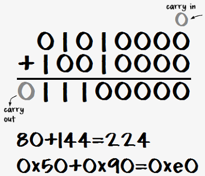
Unsigned binary addition of 80 + 44 yielding 224.

The carry flag is used as the carry-in for the operation, and the resulting carry-out value is stored in the carry flag. The carry flag can be used to chain together multiple ADC operations to perform multi-byte addition.

Ones-complement and twos-complement

The concepts of ones-complement and twos-complement are important to understand signed arithmetic. The ones complement of a number simply flips all 8 bits in the number. That is, the ones complement of N is 255-N. This is very easy to do in hardware.

The twos complement of a number is the ones complement of the number plus 1. That is, the twos complement of N is 256-N. The twos complement is very useful because adding M and the twos complement of N is the same as subtracting N from M. For example, to compute 80 - 112, simply take the twos complement of 112 (binary 10010000) and add it to 80 (binary 01010000), yielding (binary 11100000). This result is the twos complement of 32, indicating -32.
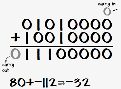
Signed binary addition of 80 and -112 yielding -32.

Note that 80+144 and 80-112 had exactly the same bit-level operations - only the interpretation of the bits was different. This is why twos complement numbers are so useful - the same addition circuit works with them.

To see why twos complement numbers work this way, consider M + (-N) or M - N

M - N
→ M - N + 256Adding 256 doesn't change the 8-bit value.
= M + (256 - N)Simple algebra.
= M + twos complement of NDefinition of twos complement.

Thus, adding the twos complement is the same as subtracting. (With the exception of the carry bit, which is affected by the extra 256. This will be discussed later)

Twos-complement signed numbers

Twos complement numbers are very useful for representing signed numbers, since a number between -128 and +127 can fit into one byte: the top bit is 0 for a normal non-negative number (0 to 127), and the top bit is 1 for a twos-complement negative number (-1 to -128). (The value of the top bit is reflected in the N (negative) status flag.)

The nice thing about signed numbers is that regular binary arithmetic yields the expected results (in most cases). That is, the processor adds or subtracts the numbers as if they are unsigned binary numbers, and the right answer occurs just by interpreting them as signed.

Another example shows that the carry is ignored with signed addition. In this case, 80 and -48 are added, yielding 32. Since 80 + (256-48) = 256 + (80-48), the "extra" 256 ends up in the carry bit.
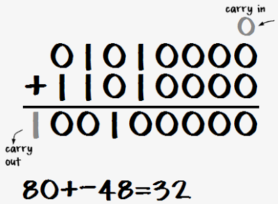
Signed addition of 80 and -48 yields a carry, which is discarded.

Unfortunately, problems can happen. For instance, 80 + 80 = 160 with unsigned arithmetic, but with signed arithmetic the result is unexpectedly -96. The problem is that 160 will fit into a byte as an unsigned number, but it is too big to store in a byte as a signed number. Since the top bit is set, it is interpreted as a negative number. To indicate this problem, the 6502 sets the overflow flag.
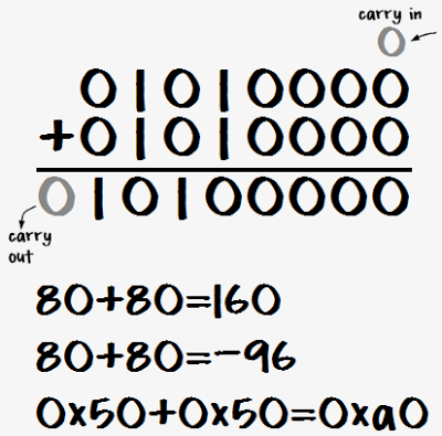
Signed addition of 80 + 80 yields overflow.

The table that explains everything about overflow

The definition of the 6502 overflow flag is that it is set if the result of a signed addition or subtraction doesn't fit into a signed byte. That is, overflow occurs if the result is > 127 or < -128. The symptom of this is adding two positive numbers and getting a negative result or adding two negative numbers and getting a positive result.

This section explores all the possible ways that overflow can occur. The following examples consider the addition of two signed numbers M and N. It is only necessary to consider the top bits of the numbers and the carry from bit 6, as shown in the diagram below, since the lower bits don't affect overflow (except by causing a carry from bit 6).
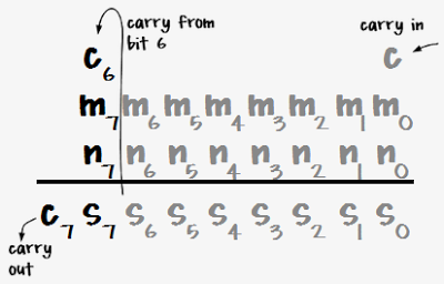
Binary addition, demonstrating the bits that affect the 6502 overflow flag.

There are 8 possibilities for these bits, as expressed in the table below. For each set of input bits, the table shows the carry out (C7), the top bit of the sum (S7), which is the sign bit, and the overflow bit V. This covers the 4 possibilities for sign of the arguments (positive + positive, positive + negative, negative + positive, negative + negative), with and without carry from bit 6. The table shows an example sum for each line, first expressed in hexadecimal, and then interpreted as unsigned addition and signed addition.

InputsOutputsExample
M7 N7 C6 C7 S7 VCarry / OverflowHexUnsignedSigned
000000No unsigned carry or signed overflow0x50+0x10=0x6080+16=9680+16=96
001011No unsigned carry but signed overflow0x50+0x50=0xa080+80=16080+80=-96
010010No unsigned carry or signed overflow0x50+0x90=0xe080+144=22480+-112=-32
011100Unsigned carry, but no signed overflow0x50+0xd0=0x12080+208=28880+-48=32
100010No unsigned carry or signed overflow0xd0+0x10=0xe0208+16=224-48+16=-32
101100Unsigned carry but no signed overflow0xd0+0x50=0x120208+80=288-48+80=32
110101Unsigned carry and signed overflow0xd0+0x90=0x160208+144=352-48+-112=96
111110Unsigned carry, but no signed overflow0xd0+0xd0=0x1a0208+208=416-48+-48=-96

A few interesting things can be noted from this table. Signed overflow (V=1) happens in two of the eight cases - when the result of adding two positive numbers overflows and ends up negative, and when the result of adding two negative numbers overflows and ends up positive. These rows are highlighted. Signed overflow will never happen when adding a positive number and a negative number, since the result will have a smaller magnitude. Unsigned carry (red in the unsigned column) happens in four of the eight cases, and is independent of signed overflow.

Formulas for the overflow flag

There are several different formulas that can be used to compute the overflow bit. By checking the eight cases in the above table, these formulas can easily be verified.

A common definition of overflow is V = C6 xor C7. That is, overflow happens if the carry into bit 7 is different from the carry out.

A second formula simply expresses the two lines that cause overflow: if the sign bits (M7 and N7) are 0 and the carry in is 1, or the sign bits are 1 and the carry in is 0:
V = (!M7&!N7&C6) | (M7&N7&!C6)

The above formula can be manipulated with De Morgan's laws to yield the formula that is actually implemented in the 6502 hardware:
V = not (((m7 nor n7) and c6) nor ((M7 nand N7) nor c6))

Overflow can be computed simply in C++ from the inputs and the result. Overflow occurs if (M^result)&(N^result)&0x80 is nonzero. That is, if the sign of both inputs is different from the sign of the result. (Anding with 0x80 extracts just the sign bit from the result.) Another C++ formula is !((M^N) & 0x80) && ((M^result) & 0x80). This means there is overflow if the inputs do not have different signs and the input sign is different from the output sign (link).

Subtraction on the 6502

The behavior of the overflow flag is fundamentally the same for subtraction, indicating that the result doesn't fit into the signed byte range -128 to 127. The 6502 has a SBC operation (subtract with carry) that subtracts two numbers and also subtracts the borrow bit. If the (unsigned) operation results in a borrow (is negative), then the borrow bit is set. However, there is no explicit borrow flag - instead the complement of the carry flag is used. If the carry flag is 1, then borrow is 0, and if the carry flag is 0, then borrow is 1. This behavior may seem backwards, but note that both for addition and subtraction, if the carry flag is set, the output is one more than if the carry flag is clear.

Defining the borrow bit in this way makes the hardware implementation simple. SBC simply takes the ones complement of the second value and then performs an ADC. To see how this works, consider M minus N minus borrow B.

M - N - BSBC of M and N with borrow B
→ M - N - B + 256Add 256, which doesn't change the 8-bit value.
= M - N - (1-C) + 256Replace B with the inverted carry flag.
= M + (255-N) + CSimple algebra.
= M + (ones complement of N) + C255 - N is the same as flipping the bits.

The following table shows the overflow cases for subtraction. It is similar to the previous table, with the addition of the B column that indicates if a borrow resulted. Unsigned operation resulting in borrow are shown in red, as are signed operations that result in an overflow.

InputsOutputsExample
M7 N7 C6 C7 BS7 VBorrow / OverflowHexUnsignedSigned
0100100Unsigned borrow but no signed overflow0x50-0xf0=0x6080-240=9680--16=96
0110111Unsigned borrow and signed overflow0x50-0xb0=0xa080-176=16080--80=-96
0000110Unsigned borrow but no signed overflow0x50-0x70=0xe080-112=22480-112=-32
0011000No unsigned borrow or signed overflow0x50-0x30=0x12080-48=3280-48=32
1100110Unsigned borrow but no signed overflow0xd0-0xf0=0xe0208-240=224-48--16=-32
1111000No unsigned borrow or signed overflow0xd0-0xb0=0x120208-176=32-48--80=32
1001001No unsigned borrow but signed overflow0xd0-0x70=0x160208-112=96-48-112=96
1011010No unsigned borrow or signed overflow0xd0-0x30=0x1a0208-48=160-48-48=-96

Comparing the above table with the overflow table for addition shows the tables are structurally similar if you take the ones-complement of N into account. As with addition, two of the rows result in overflow. However, some things are reversed compared with addition. Overflow can only occur when subtracting a positive number from a negative number or vice versa. Subtracting positive from positive or negative from negative is guaranteed not to overflow.

The formulas for overflow during addition given earlier all work for subtraction, as long as the second argument (N) is ones-complemented. Since internall subtraction is just addition of the ones-complement, N can simply be replaced by 255-N in the formulas.

Overflow myths

There are a lot of myths and confusion about the overflow flag. Since the flag is a bit difficult to understand, simple but wrong explanations are easy to find.

The most common myth is that just as the carry bit indicates a carry (or overflow) from bit 7, the overflow bit indicates a carry (or overflow) from bit 6 (example, example, example). As can be seen from the table above, sometimes a carry from bit 6 causes an overflow and sometimes it doesn't.

Another myth is that for multi-byte signed numbers, you use the overflow flag instead of the carry flag to carry from one byte to another (example). In fact, carry is still used to add/subtract multi-byte signed numbers, the same as with unsigned numbers.

It is sometimes claimed that the overflow bit is set if a result is too large to be represented in a byte (example, example). This omits the critical word signed - a signed result can be too large to fit in a byte, even if the unsigned result fits, and vice versa. Examples are in the table above.

Another confusing explanation is that the overflow flag is set when the sign bit is affected (example). The table shows that sometimes there is overflow when the sign bit is affected by bit 6 carry, and sometimes there is overflow when the sign bit is not affected.

Conclusions

This is probably more than anyone really wants to know about the overflow flag. In my next article, I discuss how overflow is implemented at the silicon level.

JavaScript on the go: Programming from your phone

Have you ever wanted to write a program when the only computer available is your phone? You can use an Android phone to write and run JavaScript programs by using a few simple tricks.

While traveling over Thanksgiving I was thinking about how the 6502 microprocessor works and wanted to analyze some Boolean logic circuits. A trivial programming task but the only computer I had was my phone.

I searched for programming languages available on Android. Python for Android looked way too complex. The Clojure REPL intrigued me but I didn't want to learn Clojure right now. Other languages seemed limited or buggy. Then I was struck by the obvious choice for a powerful and fully-supported language with graphics capabilities: JavaScript. I could run JavaScript programs in the browser if I had a way to enter them.

I downloaded DroidEdit Pro which gave me a fullscreen editor for files on my phone. Typing HTML on the phone was painful until I downloaded the Hacker's Keyboard, which makes it much easier to type special characters. The picture below shows these tools in use.

My development cycle is:

  • Edit the code in DroidEdit and save it to a local .html file.
  • Select 'Preview in Browser' from DroidEdit and test the program.
  • Upload the file to my web server using DroidEdit's SFTP support when ready.

For debugging, the trick is to use the default browser, not Chrome. Enter about:debug in the URL bar to open the JavaScript console, which is vital for debugging.

Obviously this environment isn't as powerful as a full-size keyboard and monitor and powerful editor, but it lets me program no matter where I am. I haven't got the hang of cut-and-paste in the editor, but shift-arrow seems to work better than tapping.

Here's my program in action. It wont get any style points - I rapidly lost my enthusiasm for whitespace with the tiny keyboard - but it got the job done.

I also used this development environment to show my nephew how to make web pages with HTML. He thought it was very cool that he could type HTML into the phone, hit Control-S to save, and immediately load the web page on his iPad. He's now busily learning HTML and building his own web pages.

I hope these tips help you program while on the road. Leave a comment if you have tips of your own.

Teardown of the mysterious KMS 4-port USB charger

In this article I tear down a 4-port USB charger of puzzling origin. This charger is a huge step above the $2 counterfeit chargers I examined earlier in design and manufacture, but considerably below the quality of name-brand chargers. Likewise with safety - the charger was built with some attention to safety, but appears to fall short of UL standards.

The circuit inside the KMS charger is a straightforward  flyback switching power supply. This photo shows the key components.

One puzzle about this charger is it's unclear who makes it and what model it is. The case says it's the KMS AC-09 but the circuit board says "TC09-new-V4.2". Amazon lists the brand as "Cosmos®", but I couldn't find any sign that KMS or Cosmos are actual companies. After some web searches, I think the charger is built by Guangzhou Panyu Qiaonan Saidi Electronic Factory (more) as the TC09 charger for $5.30 wholesale, or maybe HK Yingjia International, a consumer electronics manufacturer in Shenzhen (more). In any case, I'll call this the "KMS charger" since I need to call it something.

In my previous lab analysis of 12 chargers, I compared a dozen different chargers in 9 different categories, rating them from 1 to 5 'bolts' and the KMS charger came in about average in terms of performance. The results for the KMS charger are summarized below. For details on these measurements, see my previous article A dozen USB chargers in the lab).

Overall rating 3 out of 5
Vampire (idle) power usage 3 out of 5
Efficiency under load 3 out of 5
Achieves power rating 5 out of 5
Spikes in output 1 out of 5
High-frequency noise in output 4 out of 5
Ripple in output 5 out of 5
Voltage sag 1 out of 5
Current sag 1 out of 5
Regulation quality 1 out of 5

The good and the bad

Overall, this charger is much higher quality than the $2 counterfeit chargers, but considerably lower quality than name-brand chargers.

The charger provides more filtering than basic chargers, from the large input choke to the multiple output inductors. It includes X and Y capacitors for filtering.

The charger looks mostly safe, although it doesn't have UL certification and I suspect it would fail certification. The 6mm clearance between the primary and secondary looks solid. However, the transformer windings are only separated by 3mm, rather than 6mm, as I show below. (This is still much superior to the $2 chargers that have almost no separation.)

One interesting feature of the power supply is the power plug can be interchanged for use in different countries. (Some other chargers such as the HP TouchPad and Apple iPad are similar.)

The KMS TC-09 (AC09) 4-port USB charger. The power plug can be interchanged for use in different countries.

The charger has some quality issues. The power quality measurements I did in my previous article show the KMS charger has fairly poor quality output, with a lot of noise in the output.

The IC datasheet recommends 200 mm2 of foil on the IC output pins to provide cooling. I measured about 18 mm2 (less than 10% of recommended), which suggests the charger may overheat under full load.

Some of the components in the KMS charger are mounted crooked, rather than flush with the circuit board. The inductor on the right and the optoisolator on the left are two examples.

The above photo shows that the build quality of the charger is not extremely high. The inductor at the front right is very crooked, and the optocoupler at the left is somewhat crooked. While this doesn't affect the performance, it shows the assembly was rapid rather than careful. More concerning, some of the solder joints appear to be almost bridged, which could cause catastrophic failure of the charger. I also found a government report of a KMS charger catching fire, apparently due to a loose wire in the power plug.

One unique feature of the charger is the blue LEDs which cause it to emit an eerie blue glow when in use. A lot of users dislike this though (according to reviews), because the light is distracting at night.

The KMS 4-port USB charger emits an eerie blue glow when in use.

The circuit

Annotated schematic of the KMS TC-09 USB charger.

For readers interested in circuits, I have prepared the above approximate schematic (click for a larger view). The circuit is pretty straightforward compared to other chargers (look at my iPhone charger schematic for comparison). Starting at the upper left, the input AC is converted to DC by the diode bridge, and then filtered by a simple inductor-capacitor filter. This high-voltage DC is connected to the flyback transformer primary. The THX203H control IC switches the other side of the flyback transformer to ground through the current-sense resistors R12A and R12B and inductor L3. (Most chargers use a separate switching transistor, but in this charger, the transistor is inside the control IC.) The snubber circuit R2, C3, and D6 absorbs some of the high-frequency switching spikes (although looking at the output below, this circuit isn't entirely successful). The auxiliary transformer winding and D7 and C4 provide the DC power to the control IC. The optocoupler provides feedback to the IC, indicating the output voltage level.

On the secondary side, the high-speed Schottky diodes (D5) convert the transformer output to DC. This is then filtered through an inductor-capacitor filter that smooths it out. The output voltage feedback is generated by the TL431A regulator and fed into the optocoupler.[1]

Finally, the actual USB output circuitry has more components than you'd expect. For each pair of ports, four resistors set the D+ and D- voltages to indicate to devices that the charger is (pretending to be) an Apple 2A charger. Each port has a small bypass capacitor to smooth out power transients. Finally there are two blue LEDs with current-limiting resistors to provide the blue glow.

The controller IC poses a bit of a mystery. It's labeled as the THX 203H controller, which turns out to be manufactured by NanJing TongHuaXin Electronic Co, Ltd., a Chinese switching power supply chip company (details). The datasheet for this part is very hard to understand, as it is machine-translated from Chinese, for example:

The startup circuit inside IC is designed as a particular current inhalation way, so it can start up with the magnification function of the power switch tube itself.
After some more investigation, this chip seems to be the SDC603 Current Mode PWM Controller designed by SDC Semi (Shaoxing Devechip Microelectronics Co., Ltd.). This is a Chinese state-level R&D center that is part of China's Torch Plan Project to develop high-tech industries. (Also check out the SDC company song.)

The controller chip is a basic 8-pin current-mode PWM controller chip. It includes a built-in NPN power transistor, which reduces the charger part count. The chip can produce 12 watts output power.

Circuit board

The circuit board from the KMS-AC09 charger on the left and a circuit board from the HP TouchPad charger on the right. Note the much higher density of the TouchPad board.

The above picture shows the KMS charger circuit board on the left and a circuit board from the HP TouchPad charger on the right. Compact phone chargers such as the iPhone or TouchPad chargers go to amazing effort to pack the components as tightly as possible. The KMS charger on the other hand has a much more spacious design with a lot of wasted space. Since any charger with 4 USB ports is going to be fairly large, they probably figured it's not worth the effort to make the rest of the circuitry compact. The difference in density between the two circuit boards is striking, though.

A key safety feature of the KMS charger is visible in the middle of the circuit board - note the angular cut-out slot, and the empty vertical region with no circuitry. This isolates the high-voltage circuits on the right from the low-voltage output circuits on the left. The KMS charger has a safe 6mm gap and the cut-out provides additional creepage distance. Counterfeit chargers usually skip this critical safety feature, with only a millimeter or two keeping the high voltage from reaching the output and shocking the user.

You might wonder how the charger works if the high voltage and low voltage circuits are separated by a gap. The key is that any components that cross this gap must be specially designed to avoid electrical hazards. The key component is the flyback transformer, which transfers the power through magnetic fields, avoiding any direct electrical connection between the two sides. The feedback signal passes from the secondary to the primary through an optocoupler, which transmits the feedback through a light signal, again avoiding an electrical connection. Finally, a Y safety capacitor connects the primary and secondary grounds to reduce electrical noise. The design of a Y capacitor ensures it won't pass dangerous electrical currents, and won't short out even under fault conditions.

Transformer teardown

The flyback transformer is the key component of a charger and usually the largest and most expensive. The transformer is where the high input voltage is converted to the output voltage, and the two voltages are in extremely close proximity, so the safety of the transformer is critical. From the outside, you can't tell if the manufacturer saved a few cents by leaving out most of the insulation, as happens with $2 chargers. I tore apart the transformer of the KMS charger to see what's inside.

The black circle on top of the transformer seen earlier is simply a foam disk, which helps reduce transformer noise by padding the transformer against the case. If a charger makes a high-pitched noise, it's usually coming from the transformer. Power supplies are usually designed with switching frequencies higher than people can hear, but in some circumstances it's still audible, especially if you are young and haven't lost high frequency hearing.

A copper 'belly band' provides a shield around the flyback transformer.

Under the first layers of insulating tape is a copper 'belly band' which surrounds the transformer to provide noise shielding from eddy currents in the transformer.[2] This copper shielding is omitted from super-cheap transformers, showing that this charger goes beyond the minimum.

The first winding in the flyback transformer powers the internal circuits of the charger

The windings are all separated by insulating tape. Under the belly band and insulating tape is the auxiliary winding, which provides power to the control IC. You might wonder why the IC needs a separate power supply instead of using the USB power output, but this wouldn't be safe because the USB output would no longer be isolated from the input. This winding is 9 turns of wire; since the IC requires low current, the wire is fairly thin.

The first half of the primary winding in the flyback transformer. Note the 3mm white boundary tape at the right that keeps the winding away from the edge.

Above you can see half of the primary winding, which is fed by the input power. This winding has 40 turns of wire.

An interesting safety feature is the 3 mm "margin tape"[3] to the lower right of the winding, which ensures that the primary winding stays 3 mm away from the edge. I was interested to see this, since other transformers I've disassembled use triple-insulated wire instead of boundary tape. To ensure safe electrical isolation between the primary and secondary windings, either the secondary wires need to be triple-insulated, or there needs to be at least 6mm of distance between the windings. Super-small chargers don't have 3mm of extra room, so they use the more expensive triple-insulated wire. But since the KMS is larger, it uses the 3mm margin tape. I'm not an expert on safety requirements, but it looks like this transformer doesn't quite meet the requirements. Normally, the margin tape is put on both sides, so there's a total of 6mm creepage distance between the windings.[4][5] But since the tape is only on one side, the windings only have half of the required distance.

To support high current, the secondary winding in the flyback transformer is four strands of thick wire. Note the 3mm white boundary tape at the right that keeps the winding away from the edge.

The secondary winding provides the low-voltage high-current output with 8 turns of wire. In order to support 2 amps, this winding has thick wire with four strands in parallel. I haven't seen parallel strands like this before, probably because the KMS charger supplies higher power. Note the 3mm margin tape keeping the winding away from the edge.

The second half of the primary winding in the flyback transformer. The 3mm boundary tape is clearly visible at the right.

Finally, the second half of the primary winding forms the innermost layer of the transformer; this is also 40 turns of wire. The primary winding is split into two layers that surround the secondary winding for better electrical properties. Note that the primary winding is 80 turns, while the secondary output winding is 8 turns. To oversimplify a bit, this means the output will be 10 times the current of the input at 1/10 the voltage, which is how the high voltage low current input results in the low voltage high current output. The above picture gives a good view of the 3mm margin tape at the right that keeps the wire away from the edge of the core.

Measuring the charger in use

The charger is a switching power supply using a flyback transformer. How this works is the high voltage DC is switched on and off tens of thousands of times a second by the control IC. These pulses of DC are sent into the flyback transformer. A flyback transformer is different from normal transformers in that the output diode blocks power from flowing out of the transformer while power is flowing in. Instead, as the current increases, power is stored in the transformer as a magnetic field. When the input current switches off, the stored power then flows out of the transformer, providing the desired output.

By looking at the output voltage and frequency spectrum, we can determine a fair bit about how the device operates. I measured a constant 60 kHz switching frequency above 1 amp output load, but a dropping frequency for lower loads. The datasheet gives some clues to this behavior. The power supply normally operates using PWM (pulse width modulation). The switching frequency is constant, but the amount of time the power transistor is on varies. The longer it is on, the more power into the transformer and the more output power. This matches the observed behavior from 1 amp to 3.5 amps. The datasheet also describes how the switching frequency drops under low power, which matches what I observed below 1 amp.

KMS charger output (yellow)and spectrum (orange) at 2A.  Note the spectrum peaks at 60.1 kHz and harmonics.

The above oscilloscope trace illustrates the behavior when producing 2 amps. The frequency spectrum shows narrow peaks (orange) at the 60 kHz switching frequency and harmonics. The yellow output voltage shows a bunch of large spikes due to the power switching on and off - this indicates that the charger isn't filtering the output very well, letting these spikes get into the connected device.

The diagram below zooms in to show the output in more detail. Each spike is when the switching transistor turns on at 60 kHz. The output power drops as the current through the flyback transformer increases (since the transformer secondary is blocked by the diode at this time). The output then climbs when the transistor switches off and the power is transferred to the secondary.

KMS charger output at 2A, showing the effect of the switching frequency.

As the charger load increases above 3 amps, the quality of the output significantly decreases, and large 120 Hz ripple appears in the output (yellow). This is probably because the input capacitors can't store enough power to provide a constant output at this high load. Since the charger is only rated to provide 2.1 amps of output, I don't consider this a design flaw, but it's interesting to see this behavior in the output. The key result here is not to overload the charger, because the power quality gets much worse.

KMS charger output (yellow)and spectrum (orange) at 3A.  The output contains a lot of 120 Hz ripple as well as switching spikes.

The charger is designed to reduce the switching frequency under low load for efficiency. I found this feature kicks in at loads under 1 amp, with the switching frequency smoothly dropping from 60 kHz to 29 kHz at 250 mA load and even lower under no load. The graph below shows the frequency spectrum at 250 mA load. Note that the spikes are wider than the previous case since the frequency becomes more unstable when it is reduced.

The frequency spectrum of the charger under lower (250 mA) load shows the reduced 29 kHz switching frequency and harmonics.

The output waveform below at 250 mA is similar to the previous (2A) case, except at a lower frequency. Note that the output still has large spikes when the transistor switches on. The output voltage drops while the switching transistor is on and then rises while the transistor is off (due to the flyback design), so you can see below that the transistor is off most of the time at low power.

The output waveform of the charger under low (250mA) load shows a lower 29 kHz switching frequency.

Power consumption

Measuring the power consumption of a charger is tricky because the charger doesn't use power like a normal resistive load, but uses a nonlinear part of the input current. This results in a power factor lower than unity. (You might expect that the poor power factor is because the charger switches on and off thousands of times a second, but actually it's the fault of the diode bridge.) I measured the power consumption of the charger under load by measuring the instantaneous line voltage and current, computing the instantaneous power, and then computing the real power from this.[6] In the following diagrams, the input line voltage is shown in yellow, and the input current is in cyan. The instantaneous power is graphed in orange at the bottom - simply the product of the voltage and current.[7]

The oscilloscope output below shows the power usage of the charger under no load. The line input voltage (yellow) is a nice sine wave, but the current (cyan) is very irregular. There is a bump corresponding to the voltage peaks as the input diodes conduct and re-charge the filter capacitors. The remaining current oscillations are unusual - I haven't seen them in other chargers, and I expect they are due to the large input choke. From the orange line you can see that the power usage has small spikes at 120 Hz. Taking the power factor into account and computing real power shows the charger uses 180 mW when idle which is fairly high, but actually lower than the Apple iPhone charger.

KMS charger line input under no load. Yellow is 120V input, cyan is input current. Bottom shows instantaneous power.

With load applied to the charger, the power usage shoots up as shown below. I compute the power usage as 6.4 watts, while the charger is supplying 4.4 watts to the output, for an efficiency of 69%. The shape of the current curve (cyan) and power curve (orange) shows that the charger is taking line power about half the time (the big curved peaks), and not for the other half (the flat oscillations in between). This illustrates the bad power factor that switching power supplies have. (PC power supplies often use power factor correction (PFC) circuits to improve the power factor.)The yellow input voltage curve is somewhat distorted, probably due to the lame isolation transformer I used.

KMS charger line input under load. Yellow is 120V input, cyan is input current.

You might wonder what happens if you short-circuit the output of the charger. It is designed to shut down before damage occurs, rather than self-destruct. After the internal voltage drops, the charger will start up again, and repeat this cycle until the problem goes away. This is called "hiccup mode", since the charger generates hiccups of power. The oscilloscope trace below shows the power consumption of the KMS charger when shorted. Note the pulses as it start up and shuts down every 250 milliseconds.

KMS charger line input under shorted load. Yellow is 120V input, cyan is input current. Bottom shows instantaneous power. Note the 'hiccup' shutdown and restart every 250 milliseconds.

Components

For those who are interested in the components, I have some details. The two 6.8uF 400V electrolytic capacitors in the primary are made by ChengX. The two 470uF capacitors in the secondary are made by JWCO. The X capacitor is a .1uF K 275V X2 made by Dain Electronics, a Chinese manufacturer of plastic metal film capacitors, now merged with WINDAY Electronic Industrial Co Ltd. The Y1 capacitor is a JN222M 2200pF disk ceramic suppression capacitor manufactured by Jya-Nay, a Taiwanese capacitor company. There's also a blue 681J (i.e. .68nF) polyester film capacitor of unknown manufacturer; looking at the circuit board this capacitor (C7) was originally a surface-mounted device, but was replaced with a larger capacitor.

The diodes are manufactured by MIC (Master Instrument Corporation, Shanghai). Most chargers use a diode bridge to convert the AC to DC, but this charger uses four independent diodes, which are 1N4007 700V diodes. The secondary rectification uses two Schottky diodes (SR360 3 amp 60V) from MIC. The circuit board uses the unusual mounting of two diodes on top of each other soldered into the same holes. The charger also uses FR107 700V fast recovery diodes.

Like most power supplies, the charger uses a TL431A for the voltage feedback.[1] This TL431A is produced by Wing Shing Computer Components The optocoupler is an ORPC 817B optocoupler from Shenzen Orient Technology Co., Ltd. (I don't want to speculate on the cultural significance of their raising the flag over Iwo Jima company logo.)

Conclusion

The KMS charger occupies an interesting middle ground between dangerous $2 counterfeit chargers and expensive name-brand chargers. Tearing down this 4-port USB charger of unknown origin reveals details of the circuitry. It also illustrates a network of Chinese suppliers and manufacturers, most of which are hardly known in the US. On Amazon, customer ratings for this charger are split between people who love it and people who hate it, which seems reasonable given what I saw in the teardown. Thanks to Gary F. for providing the charger.

Notes and references

[1] To summarize the feedback circuit: R17 and R18 form a resistor divider on the output voltage. If the output voltage is above 5.125 volts, the TL431 control input will be above 2.5 and the TL431 conducts. This energizes the optocoupler, providing current pulling the FB pin lower. Low FB increases the duty cycle, increasing the maximum transformer current, and increasing the output voltage. If the output voltage is considerably too high, or overtemperature is sensed, the switching frequency is decreased, reducing the power transferred to the output. (This is over-simplified; the frequency response of the feedback control loop is controlled via R13, R16, C8, and C9.) An alternative is to sense voltage from the primary side, so the feedback circuit can be eliminated. This reduces the total charger cost by about 20 cents according to a report.

[2] The use of a copper "belly band" in flyback transformers is discussed in Flyback Transformer Design for the UCC28600 (page 2). It provides an electromagnetic radiation shield. The article mentions that the belly band may cause difficulties with creepage requirements and that seems to be the case with the KMS, since there is only 3mm creepage between the primary-grounded belly band and the secondary wiring.

[3] A lot of interesting information about flyback transformer design and construction is in Cookbook for do-it-yourself transformer design

[4] A discussion of how to achieve 5-6mm creepage distance by using 2.5 or 3mm margin tape is in Flyback Transformer Design for the IRIS40xx Series. Note that the margin tape must be on both sides of the winding to achieve this distance, while the KMS transformer only uses the tape on one side.

[5] Safety Considerations in Power Supply Design provides a detailed explanation of safety requirements for power supplies. It explains creepage and clearance

[6] See Understanding power factor and input current harmonics in switched mode power supplies for details on power factor, power supplies have poor power factors, and why poor power factors are a bad thing. Briefly, the power factor is due to the non-linear current through the diodes at peaks, not due to a phase shift. Real power can be measured with an oscilloscope as the average value of the instantaneous power, see Power - Real And Apparent: A Tutorial On Basic Line Power Measurements or Measuring power using the DL750.

[7] For the input power measurements it is very important to use an isolation transformer to avoid destroying your oscilloscope or shocking yourself. For my measurements, a resistor voltage divider reduced the input line voltage - the actual voltage is 11.06 times the displayed probe 1 voltage (C1, yellow). The current was measured through a 5.2 ohm shunt resistor, so the current is 1/5.2 times the displayed probe 2 voltage (C2, cyan). Combining these, the power in watts is 2.13 times the measured C1*C2 value (M1, orange).

Obama on sorting 1M integers: Bubble sort the wrong way to go

Recently StackOverflow and Hacker News discussed the question of how to sort 1 million 8-digit numbers in 1 megabyte of RAM. This reminded me of when I saw Obama in 2007 at Google - Eric Schmidt asked Obama how to sort 1 million integers as a laugh line, but Obama shocked him by answering "I think the bubble sort would be the wrong way to go." The video is pretty entertaining:

Here's the transcript:

SCHMIDT: Now, Senator, you're here at Google and I like to think of the presidency as a job interview. Now, it's hard to get a job as president. And--I mean, you're going to do a great job. It's also hard to get a job at Google. We have questions and we ask our candidates questions. And this one is from Larry Schwimmer. What--you guys think I'm kidding, it's right here.[1] What is the most efficient way to sort a million 32-bit integers?

OBAMA: Well...

SCHMIDT: Maybe--I'm sorry...

OBAMA: No, no, no, no. I think--I think the bubble sort would be the wrong way to go.

SCHMIDT: [facepalm] Come on. Who told him this? Okay. I didn't see computer science in your background.

OBAMA: We've got our spies in there.[2]

If you're wondering about the complete answer to the sorting question, see a detailed explanation.[3]

All in all, it was a very unexpected answer from Obama with perfect delivery.

Notes

[1] Nervous laughter greeted the mention of a Larry Schwimmer question, because he once asked Jimmy Carter about his UFO encounter.

[2] Eric Schmidt had asked the sorting question to John McCain on a different visit, with the expected result. See the YouTube clip of McCain's visit.

[3] The pedantic may note that Obama's question is slightly different from the Stack Overflow question since it involves 32-bit integers vs. 8 digit integers, and the memory constraint was omitted.

How to create a new schematic symbol in the Eagle editor

This tutorial describes how to create a custom schematic symbol in the CadSoft Eagle editor. It assumes that you have some familiarity with Eagle and just want to create a schematic (not a PCB), but can't find a component you need.

Creating a part is surprisingly tricky - Eagle is one of those software packages with a GUI that looks more intuitive than it is. To create a component, there are three abstractions to deal with: Symbol, Package, and Device. The Symbol is the symbol as it appears in the schematic. It must be tied to a Package, which describes the shape of how the component is physically mounted on a circuit board, in particular the pads for the pins. Finally, the Device holds the complete description of a device, including the symbol and potentially multiple packages. Thus, even if you just want a schematic symbol, you must also deal with the package and device. The following image shows important parts of the Device screen.

The Device window in Eagle. The Symbol and Package are part of the Device.

Example: Zener diode

For example, suppose you want to create a Zener diode symbol by modifying one of the existing diode symbols.

First, find a part in an existing library you want to modify, e.g. use Edit > Add, then Search for something similar. Note the name of the library and the device, e.g. "diode" and "IN4004".

Next, create your custom library by going to the Control Panel and selecting File > New > Library, or open your existing library.

In Control Panel expand the library that has the component you want to copy and find the package you want. Right click and select "Copy to Library".

Next, open the new symbol in your library: Go to Library > Symbol and select the Symbol. Or from the Device screen right click on the crosshair in the middle of the symbol and select Edit Symbol.

Finally, you can edit the symbol using the standard Eagle editor functions. To make a Zener diode, I needed to change the grid resolution to 0.025, select the angular wire bend, and then use Wire to add the "fins" to make the symbol look like a Zener diode.

Modifying an existing symbol to create a Zener diode in Eagle.

Go to File > Save As..., and save the new library.

To use this new library in your schematic, select Library > Use, and add your new library.

Improving the Symbol

The steps above are sufficient to edit and use a new component, but you may want to clean things up a bit.

To rename your symbol, go to Library > Rename, and enter a new name for the symbol.

To add a description, click on the Description link and enter a description using HTML. Typically it has <b>the title</b> <p>, and then a description.

To move the >NAME or >VALUE, use move and click on the crosshair at the lower left. You might want to temporarily reduce the grid size to get more control over the position.

Improving the Device

Go to Library > Device, and select the device.

To rename the device, use Library > Rename to rename the Device. You can also change the description as above, which is useful for searching.

To change the symbol's prefix (e.g. D1, D2, D3 for diodes), click on Prefix and enter the desired prefix.

You probably just want to have one package, so delete others by right clicking on them on the Device screen and selecting Delete.

To rename the package, go to Library > Package, and select the package. Then use Library > Rename to rename the Package. You can also change the description.

Adding new pins

If you want to add new pins to a symbol, things become more complicated, because you also need to add pads to the package and connect the pins to the pads, even if you don't care about PC boards. I recommend picking a starting symbol with the right number of pins if possible. But if not, use the following steps to add new pins.

Add the pins using Draw > Pin. You may need to rotate the pin. Right click the pin and select Properties to change the length or other property. You can enter a pin name or set Visible: Off if you don't want the pin name to show up.

To add pads, go to the Device, right click the Package, and select Edit Package. Add a Pad (anywhere) using the green circle icon.

Next you need to connect the pins and pads. Go to Library > Device and select your device. You will notice in the package pane an exclamation point in a circle. Underneath, click Connect, which will bring up the Connect panel. Select a Pin and a Pad and click Connect, until all pins are connected, and click Ok. Badk at the Device screen, you should now see a checkmark next to the Package. If you don't connect the pad to the pin, you will get "Error: Device ... has unconnected pin (G$1/P$1)!" when you try to add it to the schematic.

Creating an IC (or other component) from scratch

To create an IC, you can modify an existing IC device, a generic package from the ic-package library, or start from scratch. The existing devices are very function-specific and the ic-package symbols are kind of ugly, so you may end up needing to start from scratch. It's not too difficult and only takes a few minutes, but there are more steps than you might expect.

First, create a package with the right number of pins. Go to Library > Package, enter your package name (e.g. DIP8) after New, and click Ok. Using the green pad, drop 8 (for example) pads onto the package - the positions don't matter if you're not generating a PCB. Use Properties on each one (right click) to give the pads names 1, 2, etc.

A placeholder Package for an 8-pin IC in Eagle CAD.

Go to Library > Symbol, enter your symbol name after New (e.g. 555), and click Ok. (For this example, I'll create a 555 timer from scratch even though the library has one.) Put down all the pins for your IC, leaving plenty of room horizontally for the labels, rotating the pins as necessary. Under properties, give each pin the desired name and set length to short. Use four wires to create the outline. Put Text >NAME on the name layer (95) and Text >VALUE on the value layer (96). Add a description if you want.

Creating a custom Symbol for an IC using Eagle CAD. The pins have been labeled.

Go to Library > Device, enter your device name after New (e.g. 555) and click Ok. Click on Add, select your new symbol, and add your symbol to the device. Under the package pane, click New, select your package, and click Ok. Click Connect, and carefully connect all the pins to the right pads, so the pin numbers show up okay. (Tip: do the pins in numerical order.) Click Ok. Add a Prefix and Description if you want.

Creating a new IC device in CadSoft Eagle. The Symbol and Package have been added to the Device.

Save your library with File > Save, and it should be ready to use.

The new 555 IC symbol in use in an Eagle schematic.

Conclusion

CadSoft's Eagle PCB software is very useful for generating schematics, but the components you need are often missing. If you know the tricks, creating new symbols is not too hard, though. (If you want to create parts for a PCB, see Creating a new device in Eagle or Instructables or Sparkfun's tutorial.) I wrote this tutorial mainly for my own benefit, but I hope others find it useful too. Please leave a comment if you find errors or have additional suggestions.

Spectral analysis with the Tektronix 5000 oscilloscope

Many oscilloscopes have advanced spectral analysis features that perform Fourier Transforms on measured signals to generate a frequency spectrum. This article provides a tutorial on how to use these features on the Tektronix 5000 oscilloscope, assuming you already understand what a frequency spectrum is.

Getting started

The basic idea is you measure a waveform with the oscilloscope and use spectral analysis to see the frequency spectrum of this waveform. The first step is to display the desired input, which I assume you know how to do.

Next, to start Spectral analysis, go to Math -> Spectral Setup.... Choose Magnitude, Channel 1, and Ok. This will display the spectrum of channel 1 as the Math1 curve.

controls for spectral analysis

You'll discover there are a dozen settings with complex interactions. There are three columns of controls: Time Controls (Record Length, Sample Rate, Duration, and Resolution), Gating Controls (Gate Position, Gate Duration, and Gate Length), and Frequency Controls (Center Frequency, Frequency Span, and Resolution Bandwidth).

The Time Controls select how much data is collected. Record Length is the number of data points collected, Sample Rate is the sampling frequency, Duration is the time interval collected, and Resolution is the time between samples.

The Gating Controls select which data is actually used for the FFT, since you can use less data than you are collecting. Gate Duration is the sub-region of the Duration that is processed, and Gate Length is the number of samples in the Gate Duration. The Gate Duration is the interval between vertical yellow lines in the display.

The Frequency Controls select what results are displayed. The displayed frequency spectrum is centered on Center Frequency with total width of Frequency Span. Clicking Full will make the Frequency Span as large as possible with the existing settings. The Resolution Bandwidth specifies how detailed the frequency spectrum is, so smaller is "better".

Controlling the parameters

By clicking on a parameter, two of the parameters will be assigned to multi-function knobs, indicated by two circles next to the parameter and a green line indicating which knob controls it. Note that due to interdependencies between the parameters, adjusting one parameter can change other parameter. Also, the range of a parameter may be constrained by other parameters. You can also click on the number and manually entera value, or often set it to the minimum or maximum value, which can be convenient.

Advice

First figure out the maximum frequency you're interested in, the time period you're interested in, and the minimum frequency resolution you want.

Set the Sample Rate to at least twice the maximum frequency of interest. (Note that Sample Rate is basically in Hertz; s means samples per second, not seconds for Sample Rate. Resolution is the reciprocal of Sample Rate.)

Duration controls the Resolution Bandwidth; a longer Duration yields a smaller (better) Resolution Bandwidth. At least two cycles of the lowest frequency of interest must fit into the Duration. The Duration should include several cycles of the waveform of interest. Note that if the Duration is multiple seconds, it will inconveniently take a long time to collect data before showing you the waveform. And if the Record Length is long, the processing time will be long.

The Record Length will be determined from the Sample Rate and Duration, Generally around 20,000 is a good value. A much smaller value won't give you good frequency resolution, and a much larger value will slow down processing.

The Resolution control is usually the best Time control to adjust, since the others interact with each other in annoying ways.

For the Gating controls, I recommend leaving the Window Type at Gaussian and the Gate Position at 0 unless you know you want to do something else. you probably want the Gate Duration to be as large as the Duration, or else you're wasting data and getting a worse Resolution Bandwidth. If the Gate Duration is smaller than the Duration, it will be displayed as vertical yellow lines that show the part of the waveform that is getting processed.

For the Frequency Controls, you probably want Center Frequency to be half of Frequency Span; this means that you're seeing the full spectrum starting at 0. It's very easy for Center Frequency to get larger, which means you're looking at a random region in the middle of the middle of the spectrum, so you may need to continually set the Center Frequency back to the minimum value. It usually works best to modify freqency by increasing the Frequency Span and decreasing the Center Frequency, to keep the two in sync. If the frequency spectrum looks like sine waves rather than spikes, the Resolution Bandwidth is probably too large.

Be careful you don't clip the input waveform on the top of the screen, as this will mess up the spectrum. Set the vertical scale so it fits.

Example: Square wave frequency spectrum

An easy example is to generate the frequency spectrum of the 1kHz calibration square wave. (Just connect the probe to the calibration output on the oscilloscope.) The theoretical spectrum for a square wave is spikes for the odd harmonics, with height proportional to 1/n. Specifically, a 1 volt peak-to-peak square wave will have harmonics of 2/π/n volts peak-to-peak for odd n, or 0.63V and 0.21V for the first two (odd) harmonics. Converting the harmonics to RMS voltages by dividing by sqrt(2) yields theoretical RMS voltages of 0.450V and 0.150V for the first two harmonics.

frequency spectrum of square wave

The above picture shows a first attempt at generating the frequency spectrum (orange) of the square wave (yellow). The duration is too short - it only includes 4 cycles of the waveform, so the Resolution Bandwidth is large (500Hz). The result is the spikes are spread out into sine-like curves and the spectrum is not very distinct.

square wave spectrum showing large frequency span

In the above picture, the duration has been increased to 40mS, so 40 cycles of the waveform are included. With a long duration, the Resolution Bandwidth is narrow (50Hz), so the harmonics are narrow spikes as desired. However, with a wide Frequency Span, the harmonics are crammed together and hard to see.

spectrum zoomed in with decreased frequency span

To see the spectrum in more detail (zoomed-in), decrease the Frequency Span, which gives more detail of the spectrum. However, note that the spikes are all almost the same size. since the Center Frequency is not half of the Frequency Span, we're looking at the middle of spectrum (3.125kHz to 18.75kHz), rather than starting at 0Hz. It is very easy to accidentally shift the spectrum range and get confused about what you're seeing, so be cautious.

spectrum of square wave

Finally, with the Center Frequency set to half of the Frequency Span, the image above shows the spectrum starting at 0. The frequency scale (Math1) is 1.56kHz per grid line, so the spikes are at 1kHz, 3kHz, 5kHz, etc. as expected. (Inconveniently, I can't find a way to get the frequency scale to be round numbers.)

spectral analysis showing Gate Duration

With the Gate Duration decreased, note the vertical yellow lines showing the gate region. Only the signal between the lines is being processed. This increases the Resolution Bandwidth (i.e. makes it worse), so the harmonics are now considerably wider than the spikes seen previously.

The theory behind dB and dBm

The dB and dBm scales are logarithmic, which allows harmonics with a large range of powers to be displayed: when the power increases by a factor of 10, the dB measurement increases by 10 dB. dB is measured against an arbitrary reference power, so the fomula is dB = 10 * log10(power / powerreference). Since the oscilloscope measures voltage, not power, the fomula actually used is dB = 20 * log(V / Voffset), for a fixed offset voltage. Voffset corresponds to 0 dB. Since power is proportional to V^2, increasing the voltage by a factor of 10 increases the power by a factor of 100 which increases the dB value by 20 dB.

For the dBm scale, the offset voltage is set to 223.6mV. Although this value may seem random, there is an explanation. The definition of dBm is 10*log(power), where power is the RMS power in milliwatts. dBm is defined with a fixed impedance of 50Ω. (Other fields use different impedances for dBm, for example audio work uses 600Ω.) Working through some math yields Vref = sqrt(50Ω*1mW) = 223.6mV. (See Wikipedia for more explanation of dBm.)

The oscilloscope's dB and dBm settings

On the oscilloscope, the Spectral controls affecting the dB display are Level, Offset, and Scale. Scale is the number of dB per division. Level controls the position of the M1 zero dB position, measured in dB below the top of the screen. Finally, Offset defines what voltage is 0 dB. The default Offset is 223.6 mV as explained above. Increasing Offset shifts the spectrum down with respect to the M1 zero position. For instance, Offset of 707.09 mV shifts the curve down by 10 dB, and 2.236V shifts the curve down 20 dB.

The scale values for Math1 are used to display the dBm curve. The vertical scale shows the number of dBm per division, and the horizontal scale shows the frequency per division. The M1 indicator on the left shows the position of 0 dBM. Note that dBm values can be positive or negative.

In the Math controls, the controls are Pos and Scale - Pos is the number of divisions that M1 (0 dBm) is above the center line, so Level = (4 - pos) * Scale.

On the oscilloscope, there are few differences between the dB and dBm settings. dBm defaults to centering the spectrum on the screen (which generally puts M1 high up), and using 223.6mV as the offset. dB defaults to centering M1 on the screen (which generally puts the spectrum lower). If you adjust the Level, Offset, and Scale to be equal, the dBm and dB settings give the same results, so they aren't fundamentally different. The default Level and Scale are usually ugly numbers; you can adjust them to round values.

The square wave spectrum gives an example of dBm in use. Looking at the theoretical values for the square wave, the first harmonic of 0.45V is 20*log(450mV/223.6mV) = 6.1dBm and the second odd harmonic of 0.15V is 20*log(150mV/223.6mV) is -3.5dBm. Looking at the measured harmonics, the first is about 0.4 divisions above the M1 mark, and the second is about 0.2 divisions below the mark. Since the scale is 15.1dBM / division, this yields measured values of 6dBm and -3dBm, close to the theoretical values.

Understanding the linear scale

spectral analysis showing linear scale

The linear scale displays the RMS voltage of each harmonic. The M1 arrow at the left indicates the 0 position (which can be adjusted). The Math1 Scale shows how many mV per vertical division, and how many kiloHertz per horizontal division. Position shows the number of divisions M1 is above the center line.

Changing the scale to Linear shows how the harmonics in the example drop off rapidly as 1/N: 1, 1/3, 1/5, 1/7, etc. (Note that higher-order harmonics are much harder to see with the linear scale than with the dB scale.) Aligning cursors with the first two harmonics indicate the first harmonic is 1kHz at 445.4mV, and the third harmonic is 3kHz at 144.6mV. These values are close to the theoretical values of 450mV and 150mV. The values can also be determined from the display using the scale. In this example, the Math1 scale is 117mV per vertical division and 2.5kHz per horizontal division. The first harmonic is about 3.8 divisions above the 0 level, which works out to 445mV.

Reading voltage and frequency values can be inconvenient because the scale usually ends up with inconveniently non-round values per division. Using a math cursor, as above, make this easier. The cursors are accessed under Cursors > Cursor Setup, and then moved to the desired positions.

Some relations between the controls

Many of the control values are related to other values by simple equations. The following relationships may help understand the controls.
  • 1 / Sample Rate = Resolution.
    Resolution is just the time between samples.
  • Record Length = Sample Rate * Duration.
    Record Length is the total number of samples collected.
  • Gate Length = Gate Duration * Sample Rate.
    Gate Length is the total number of samples processed.
  • Gate Duration ≤ Duration.
    The Gate Duration must be smaller than the total Duration.
  • Gate Length ≤ Record Length.
    The Gate Length must be smaller than the total Length.
  • Center Frequency ≥ Frequency Span / 2.
    The minimum frequency in the range must be positive.
  • Resolution Bandwidth = 2 / Gate Duration.
    The slowest waveform must fit into the duration at least twice.
  • Freq Span ≤ Sample Rate / 2.
    The Nyquist limit requires at least two samples at the highest frequency.
  • Spectral Level = (4 - Math Pos) * Scale
    Level is measured from the top of the screen, 4 divisions above the center line.

For the official Tektronix documentation, see Defining a Speactral Math Waveform in the TDS5000B Series Oscilloscopes Online Help, page 291. Also see TDS5000B Series Quick Start User Manual, page 75.

This tutorial is mostly for my own reference, so I can remember how to use the oscilloscope in the future, but hopefully it will be of benefit to some other readers.