Interesting double-poly latches inside AMD's vintage LANCE Ethernet chip

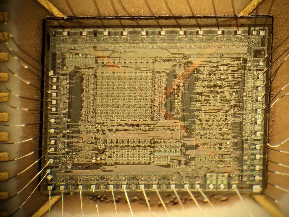
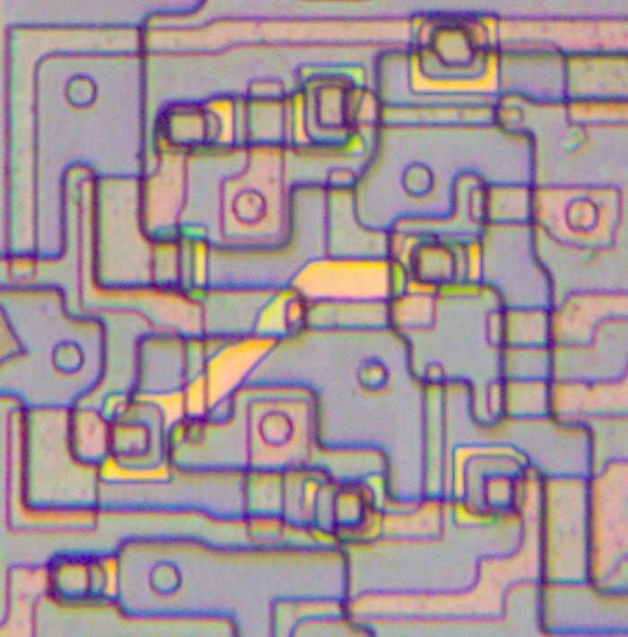
I've studied a lot of chips from the 1970s and 1980s, so I usually know what to expect. But an Ethernet chip from 1982 had something new: a strange layer of yellow wiring on the die. After some study, I learned that the yellow wiring is a second layer of resistive polysilicon, used in the chip's static storage cells and latches.

A closeup of the die of the LANCE chip. The metal has been removed to show the layers underneath.

A closeup of the die of the LANCE chip. The metal has been removed to show the layers underneath.

The die photo above shows a closeup of a latch circuit, with the diagonal yellow stripe in the middle. For this photo, I removed the chip's metal layer so you can see the underlying circuitry. The bottom layer, silicon, appears gray-purple under the microscope, with the active silicon regions slightly darker and bordered in black. On top of the silicon, the pink regions are polysilicon, a special type of silicon. Polysilicon has a critical role in the chip: when it crosses active silicon, polysilicon forms the gate of a transistor. The circles are contacts between the metal layer and the underlying silicon or polysilicon. So far, the components of the chip match most NMOS chips of that time. But what about the bright yellow line crossing the circuit diagonally? That was new to me. This second layer of polysilicon provides resistance. It crosses over the other layers, connected to the silicon at the ends with a complex ring structure.

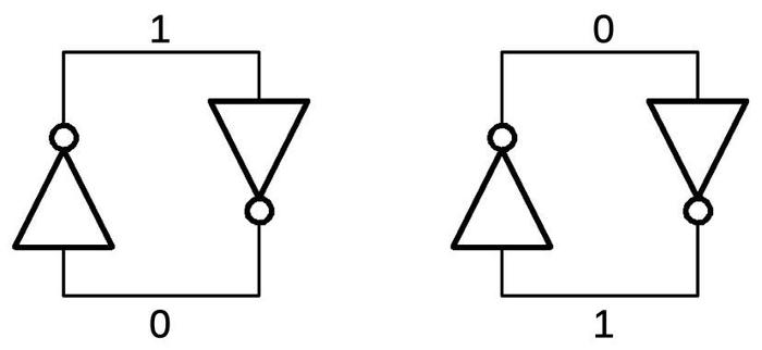
Why would you want high-resistance wiring in your digital chip? To understand this, let's first look at how a bit can be stored. An efficient way to store a bit is to connect two inverters in a loop, as shown below. Each inverter sends the opposite value to the other inverter, so the circuit will be stable in two states, holding one bit: a 1 or a 0.

Two cross-coupled inverters can store either a 0 or a 1 bit.

Two cross-coupled inverters can store either a 0 or a 1 bit.

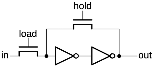
But how do you store a new value into the inverter loop? There are a few techniques. One is to use pass transistors to break the loop, allowing a new value to be stored. In the schematic below, if the hold signal is activated, the transistor turns on, completing the loop. But if hold is dropped and load is activated, a new value can be loaded from the input into the inverter loop.

A latch, controlled by pass transistors.

A latch, controlled by pass transistors.

An alternative is to use a weak inverter that produces a low-current output. In this case, the input signal can simply overpower the value produced by the inverter, forcing the loop into a new state. The advantage of this circuit is that it eliminates the "hold" transistor. However, a weak inverter turns out to be larger than a regular inverter, negating much of the space saving.1 (The Intel 386 processor uses this type of latch.)

A latch using a weak inverter.

A latch using a weak inverter.

A third alternative, used in the Ethernet chip, is to use a resistor for the feedback, limiting the current.2 As in the previous circuit, the input can overpower the low feedback current. However, this circuit is more compact since it doesn't require a larger inverter. The resistor doesn't require additional space since it can overlap the rest of the circuitry, as shown in the photo at the top of the article. The disadvantage is that manufacturing the die requires additional processing steps to create the resistive polysilicon layer.

A latch using a resistor for feedback.

A latch using a resistor for feedback.

In the Ethernet chip, this type of latch is used in many circuits. For example, shift registers are built by connecting latches in sequence, controlled by the clock signals. Latches are also used to create binary counters, with the latch value toggled when the lower bits produce a carry.

The SRAM cell

It would be overkill to create a separate polysilicon layer just for a few latches. It turns out that the chip was constructed with AMD's "64K dynamic RAM process". Dynamic RAM uses tiny capacitors to store data. In the late 1970s, dynamic RAM chips started using a "double-poly" process with one layer of polysilicon to form the capacitors and a second layer of polysilicon for transistor gates and wiring (details).

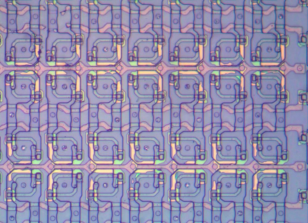
The double-poly process was also useful for shrinking the size of static RAM.3 The Ethernet chip contains several blocks of storage buffers for various purposes. These blocks are implemented as static RAM, including a 22×16 block, a 48×9 block, and a 16×7 block. The photo below shows a closeup of some storage cells, showing how they are arranged in a regular grid. The yellow lines of resistive polysilicon are visible in each cell.

A block of 28 storage cells in the chip. Some of the second polysilicon layer is damaged.

A block of 28 storage cells in the chip. Some of the second polysilicon layer is damaged.

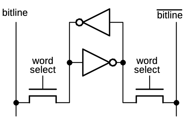
A static RAM storage cell is roughly similar to the latch cell, with two inverters in a loop to store each bit. However, the storage is arranged in a grid: each row corresponds to a particular word, and each column corresponds to the bits in a word. To select a word, a word select line is activated, turning on the pass transistors in that row. Reading and writing the cell is done through a pair of bitlines; each bit has a bitline and a complemented bitline. To read a word, the bits in the word are accessed through the bitlines. To write a word, the new value and its complement are applied to the bitlines, forcing the inverters into the desired state. (The bitlines must be driven with a high-current signal that can overcome the signal from the inverters.)

Schematic of one storage cell.

Schematic of one storage cell.

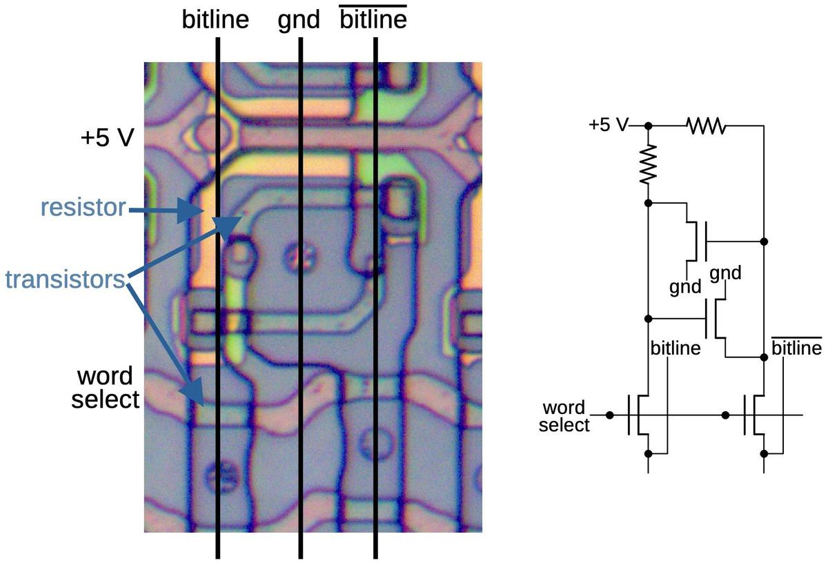
The diagram below shows the physical layout of one memory cell, consisting of two resistors and four transistors. The black lines indicate the vertical metal wiring that was removed. The schematic on the right corresponds to the physical arrangement of the circuit. Each inverter is constructed from a transistor and a pull-up resistor, and the inverters are connected into a loop. (The role of these resistors is completely different from the feedback resistors in the latch.) The two transistors at the bottom are the pass transistors that provide access to the cell for reads or writes.

One memory cell static memory cell as it appears on the die, along with its schematic.

One memory cell static memory cell as it appears on the die, along with its schematic.

The layout of this storage cell is highly optimized to minimize its area. Note that the yellow resistors take almost no additional area, as they overlap other parts of the cell. If constructed without resistors, each inverter would require an additional transistor, making the cell larger.

To summarize, although the double-poly process was introduced for DRAM capacitors, it can also be used for SRAM cell pull-up resistors. Reducing the size of the SRAM cells was probably the motivation to use this process for the Ethernet chip, with the latch feedback resistors a secondary benefit.

The Am7990 LANCE Ethernet chip

I'll wrap up with some background on the AMD Ethernet chip. Ethernet was invented in 1973 at Xerox PARC and became a standard in 1980. Ethernet was originally implemented with a board full of chips, mostly TTL. By the early 1980s, companies such as Intel, Seeq, and AMD introduced chips to put most of the circuitry onto VLSI chips. These chips reduced the complexity of Ethernet interface hardware, causing the price to drop from $2000 to $1000.

The chip that I'm examining is AMD's Am7990 LANCE (Local Area Network Controller for Ethernet). This chip implemented much of the functionality for Ethernet and "Cheapernet" (now known as 10BASE2 Ethernet). The chip handles serial/parallel conversion, computing the 32-bit CRC checksum, handling collisions and backoff, and recognizing desired addresses. The chip also provides DMA access for interfacing with a microcomputer.

The chip doesn't handle everything, though. It was designed to work with an Am7992 Serial Interface Adapter chip that encodes and decodes the bitstream using Manchester encoding. The third chip was the Am7996 transceiver that handled the low-level signaling and interfacing with the coaxial network cable, as well as detecting collisions if two nodes transmitted at the same time.

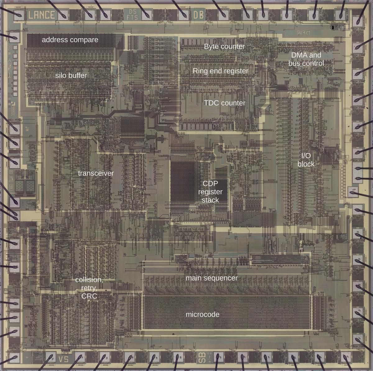
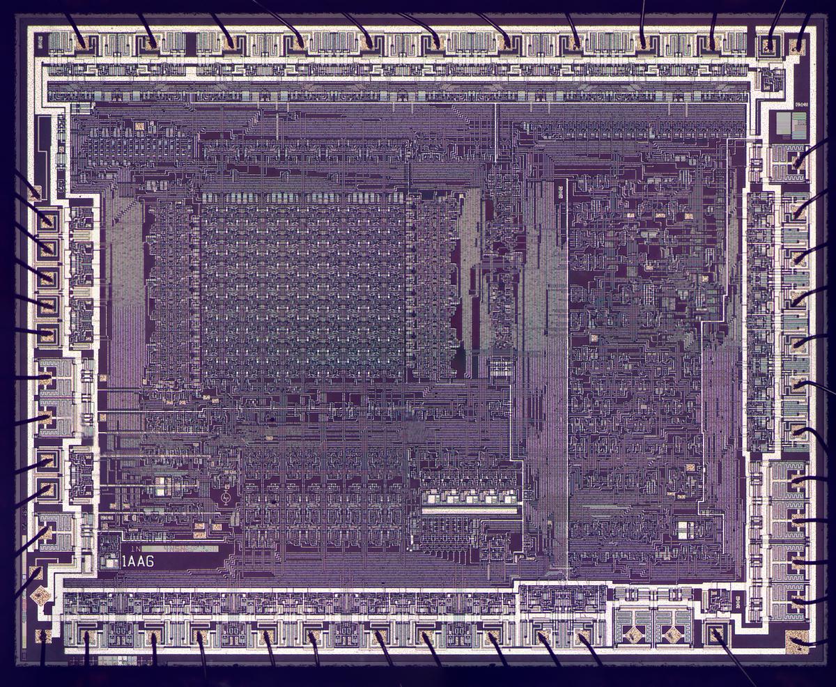
The LANCE chip is fairly complicated. The die photo below shows the main functional blocks of the chip. The chip is controlled by the large block of microcode ROM in the lower right. The large dark rectangles are storage, implemented with the static RAM cells described above. The chip has 48 pins, connected by tiny bond wires to the square pads around the edges of the die.

Main functional blocks of the LANCE chip.

Main functional blocks of the LANCE chip.

Thanks to Robert Garner for providing the AMD LANCE chip and information, thanks to a bunch of people on Twitter for discussion, and thanks to Bob Patel for providing the functional block labeling and other information. For more, follow me on Twitter @kenshirriff or RSS for updates. I'm also on Mastodon occasionally as @[email protected].

Notes and references

  1. It may seem contradictory for a weak inverter to be larger than a regular inverter, since you'd expect that the bigger the transistor, the stronger the signal. It turns out, however, that creating a weak signal requires a larger transistor, due to how MOS transistors are constructed. The current from a transistor is proportional to the gate's width divided by the length. Thus, to create a more powerful transistor, you increase the width. But to create a weak transistor, you can't decrease the width because the minimum width is limited by the manufacturing process. Thus, you need to increase the gate's length. The result is that both stronger and weaker transistors are larger than "normal" transistors. 

  2. You might worry that the feedback resistor will wastefully dissipate power. However, the feedback current is essentially zero because NMOS transistor gates are essentially insulators. Thus, the resistor only needs to pass enough current to charge or discharge the gate. 

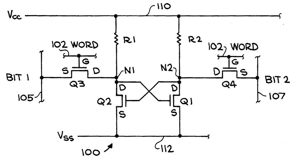
  3. An AMD patent describes the double-poly process as well as the static RAM cell; I'm not sure this is the process used in the Ethernet chip, but I expect the process is similar. The diagram below shows the RAM cell with its two resistors. The patent describes how the resistors and second layer of wiring are formed by a silicide/polysilicon ("inverted polycide") sandwich. (The silicide is a low-resistance compound of tantalum and silicon or molybdenum and silicon.) Specifically, the second layer consists of a buffer layer of polysilicon, a thicker silicide layer, and another layer of polysilicon forming the low-resistance "sandwich". Where resistance is desired, the bottom two layers of "sandwich" are removed during fabrication to leave just a layer of polysilicon. This polysilicon is then doped through implantation to give it the desired resistance.

    The static RAM cell from patent 4569122, "Method of forming a low resistance quasi-buried contact".

    The static RAM cell from patent 4569122, "Method of forming a low resistance quasi-buried contact".

    The patent also describes using the second layer of polysilicon to provide a connection between silicon and the main polysilicon layer. Chips normally use a "buried contact" to connect silicon and polysilicon, but the patent describes how putting the second layer of polysilicon on top reduces the alignment requirements for a low-resistance contact. I think this explains the yellow ring of polysilicon around all the silicon/polysilicon contacts in the chip. (These rings are visible in the die photo at the top of the article.) Patent 4581815 refines this process further.


The transparent chip inside a vintage Hewlett-Packard floppy drive

While repairing an eight-inch HP floppy drive, we found that the problem was a broken interface chip. Since the chip was bad, I decapped it and took photos. This chip is very unusual: instead of a silicon substrate, the chip is formed on a base of sapphire, with silicon and metal wiring on top. As a result, the chip is transparent as you can see from the gold "X" visible through the die in the photo below.

The PHI die as seen through an inspection microscope. Click this image (or any other) for a larger version.

The PHI die as seen through an inspection microscope. Click this image (or any other) for a larger version.

The chip is a custom HP chip from 1977 that provides an interface between HP's interface bus (HP-IB) and the Z80 processor in the floppy drive controller. HP designed this interface bus as a low-cost bus to connect test equipment, computers, and peripherals. The chip, named PHI (Processor-to-HP-IB Interface), was used in multiple HP products. It handles the bus protocol and buffered data between the interface bus and a device's microprocessor.1 In this article, I'll take a look inside this "silicon-on-sapphire" chip, examine its metal-gate CMOS circuitry, and explain how it works.

Silicon-on-sapphire

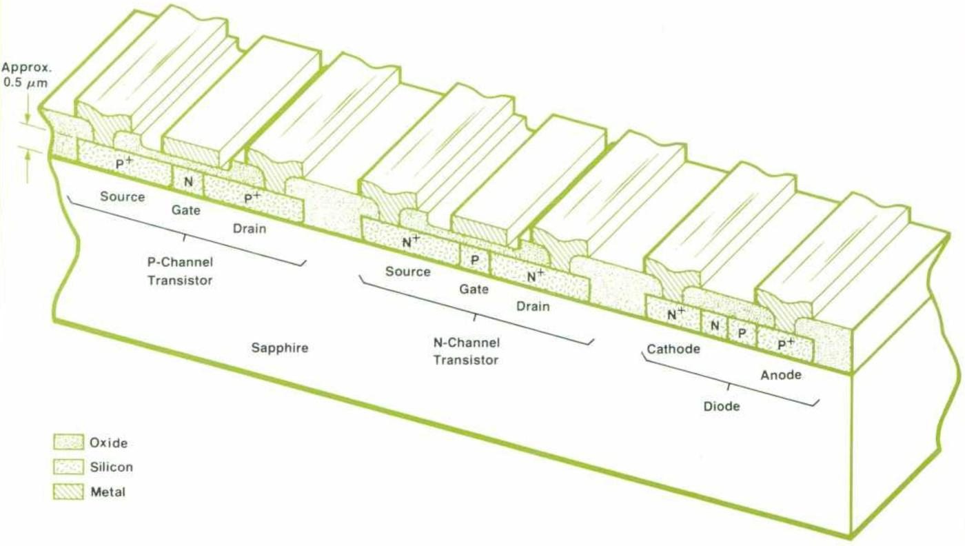
Most integrated circuits are formed on a silicon wafer. Silicon-on-sapphire, on the other hand, starts with a sapphire substrate. A thin layer of silicon is built up on the sapphire substrate to form the circuitry. The silicon is N-type, and is converted to P-type where needed by ion implantation. A metal wiring layer is created on top, forming the wiring as well as the metal-gate transistors. The diagram below shows a cross-section of the circuitry.

Cross-section from HP Journal, April 1977.

Cross-section from HP Journal, April 1977.

The important thing about silicon-on-sapphire is that silicon regions are separated from each other. Since the sapphire substrate is an insulator, transistors are completely isolated, unlike a regular integrated circuit. This reduces the capacitance between transistors, improving performance. The insulation also prevents stray currents, protecting against latch-up and radiation.

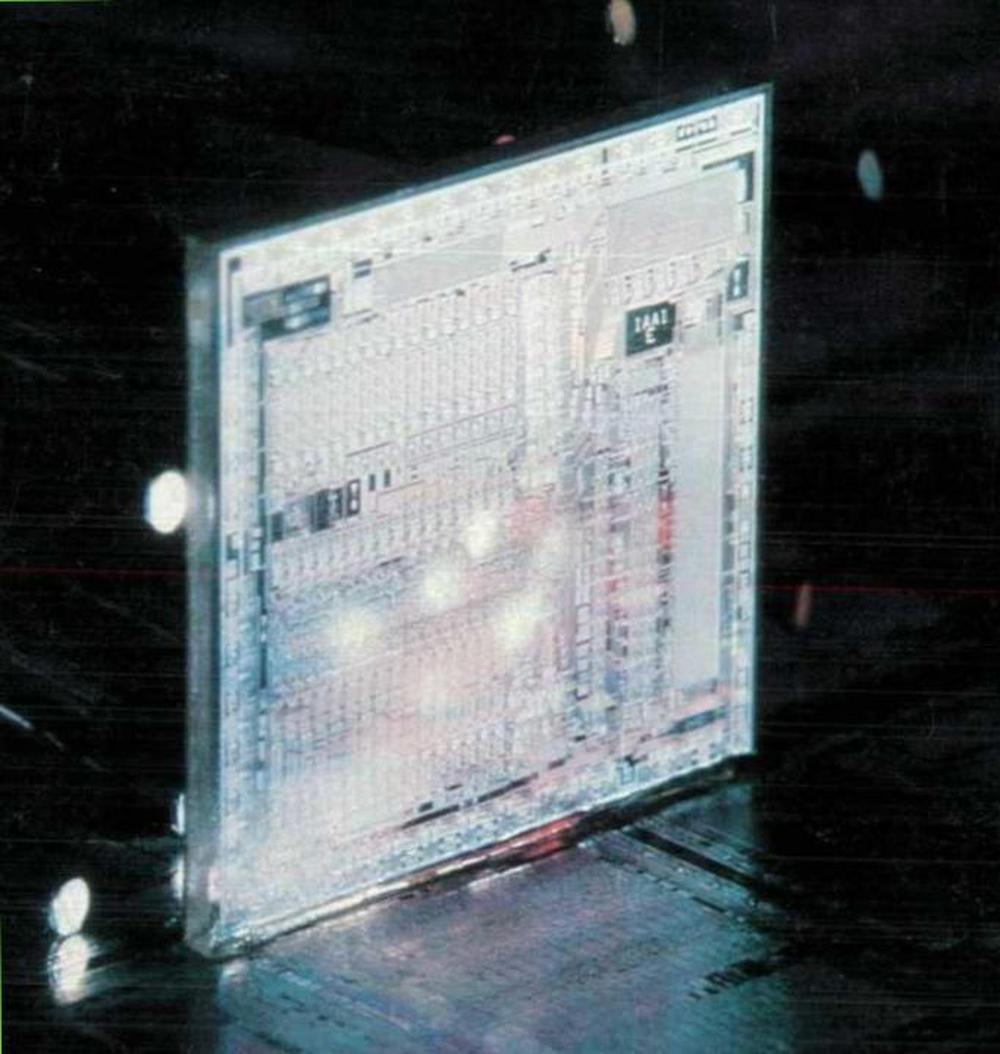
An HP MC2 die, illuminated from behind with fiber optics. From Hewlett-Packard Journal, April 1977.

An HP MC2 die, illuminated from behind with fiber optics. From Hewlett-Packard Journal, April 1977.

Silicon-on-sapphire integrated circuits date back to research in 1963 at Autonetics, an innovative but now-forgotten avionics company that produced guidance computers for the Minuteman ICBMs, among other things. RCA developed silicon-on-sapphire integrated circuits in the 1960s and 1970s such as the CDP1821 silicon-on-sapphire 1K RAM. HP used silicon-on-sapphire for multiple chips starting in 1977, such as the MC2 Micro-CPU Chip. HP also used SOS for the three-chip CPU in the HP 3000 Amigo (1978), but the system was a commercial failure. The popularity of silicon-on-sapphire peaked in the early 1980s and HP moved to bulk silicon integrated circuits for calculators such as the HP-41C. Silicon-on-sapphire is still used in various products, such as LEDs and RF applications, but is now mostly a niche technology.

Inside the PHI chip

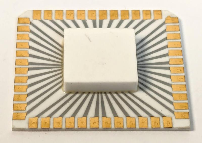
HP used an unusual package for the PHI chip. The chip is mounted on a ceramic substrate, protected by a ceramic cap. The package has 48 gold fingers that press into a socket. The chip is held into the socket by two metal spring clips.

Package of the PHI chip, showing the underside. The package is flipped over when mounted in a socket.

Package of the PHI chip, showing the underside. The package is flipped over when mounted in a socket.

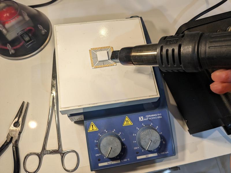
Decapping the chip was straightforward, but more dramatic than I expected. The chip's cap is attached with adhesive, which can be softened by heating. Hot air wasn't sufficient, so we used a hot plate. Eric tested the adhesive by poking it with an X-Acto knife, causing the cap to suddenly fly off with a loud "pop", sending the blade flying through the air. I was happy to be wearing safety glasses.

Decapping the chip with a hotplate and hot air.

Decapping the chip with a hotplate and hot air.

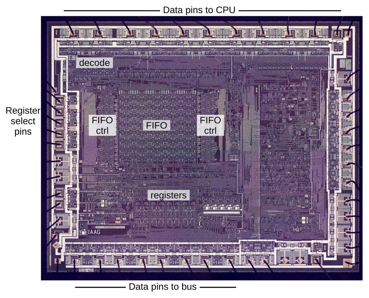
After decapping the chip, I created the high-resolution die photo below. The metal layer is clearly visible as white lines, while the silicon is grayish and the sapphire appears purple. Around the edge of the die, bond wires connect the chip's 48 external connections to the die. Slightly upper left of center, a large regular rectangular block of circuitry provides 160 bits of storage: this is two 8-word FIFO buffers, passing 10-bit words between the interface bus and a connected microprocessor. The thick metal traces around the edges provide +12 volts, +5 volts, and ground to the chip.

Die photo of the PHI chip, created by stitching together microscope photos. Click for a much larger image.

Die photo of the PHI chip, created by stitching together microscope photos. Click for a much larger image.

Logic gates

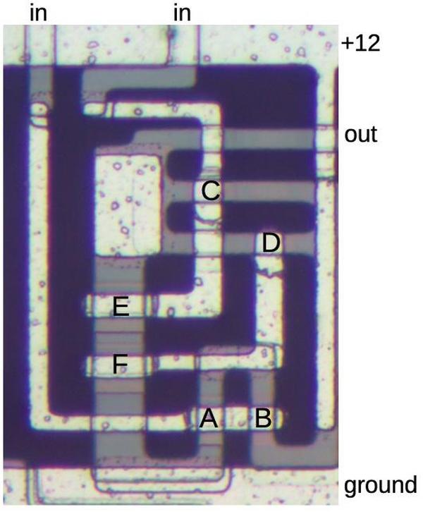
Circuitry on this chip has an unusual appearance due to the silicon-on-sapphire implementation as well as the use of metal-gate transistors, but fundamentally the circuits are standard CMOS. The photo below shows a block that implements an inverter and a NAND gate. The sapphire substrate appears as dark purple. On top of this, the thick gray lines are the silicon. The white metal on top connects the transistors. The metal can also form the gates of transistors when it crosses silicon (indicated by letters). Inconveniently, metal that contacts silicon, metal that crosses over silicon, and metal that forms a transistor all appear very similar in this chip. This makes it more difficult to determine the wiring.

This diagram shows an inverter and a NAND gate on the die.

This diagram shows an inverter and a NAND gate on the die.

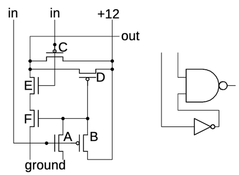
The schematic below shows how the gates are implemented, matching the photo above. The metal lines at the top and bottom provide the power and ground rails respectively. The inverter is formed from NMOS transistor A and PMOS transistor B; the output goes to transistors D and F. The NAND gate is formed by NMOS transistors E and F in conjunction with PMOS transistors C and D. The components of the NAND gate are joined at the square of metal, and then the output leaves through silicon on the right. Note that signals can only cross when one signal is in the silicon layer and one is in the metal layer. With only two wiring layers, signals in the PHI chip must often meander to avoid crossings, wasting a lot of space. (This wiring is much more constrained than typical chips of the 1970s that also had a polysilicon layer, providing three wiring layers in total.)

This schematic shows how the inverter and a NAND gate are implemented.

This schematic shows how the inverter and a NAND gate are implemented.

The FIFOs

The PHI chip has two first-in-first-out buffers (FIFOs) that occupy a substantial part of the die. Each FIFO holds 8 words of 10 bits, with one FIFO for data being read from the bus and the other for data written to the bus. These buffers help match the bus speed to the microprocessor speed, ensuring that data transmission is as fast as possible.

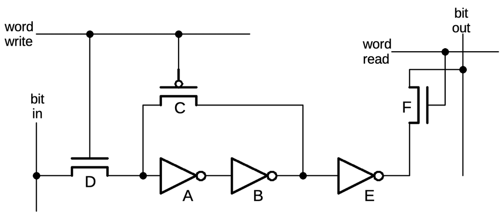
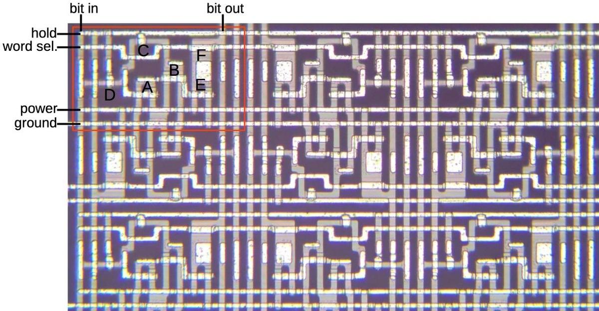
Each bit of the FIFO is essentially a static RAM cell, as shown below. Inverters A and B form a loop to hold a bit. Pass transistor C provides feedback so the inverter loop remains stable. To write a word, 10 bits are fed through vertical bit-in lines. A horizontal word write signal is activated to select the word to update. This disables transistor C and turns on transistor D, allowing the new bit to flow into the inverter loop. To read a word, a horizontal word read line is activated, turning on pass transistor F. This allows the bit in the cell to flow onto the vertical bit-out line, buffered by inverter E. The two FIFOs have separate lines so they can be read and written independently.

One cell of the FIFO.

One cell of the FIFO.

The diagram below shows nine FIFO cells as they appear on the die. The red box indicates one cell, with components labeled to match the schematic. Cells are mirrored vertically and horizontally to increase the layout density.

Nine FIFO cells as they appear on the die.

Nine FIFO cells as they appear on the die.

Control logic (not shown) to the left and right of the FIFOs manages the FIFOs. This logic generates the appropriate read and write signals so data is written to one end of the FIFO and read from the other end.

The address decoder

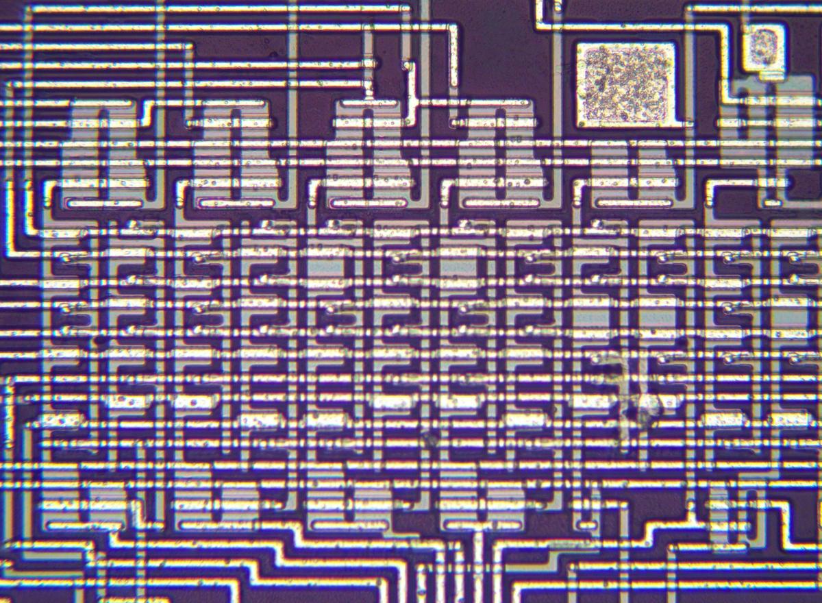
Another interesting circuit is the decoder that selects a particular register based on the address lines. The PHI chip has eight registers, selected by three address lines. The decoder takes the address lines and generates 16 control lines (more or less), one to read from each register, and one to write to each register.

A die photo of the address decoder.

A die photo of the address decoder.

The decoder has a regular matrix structure for efficient implementation. Row lines are in pairs, with a line for each address bit input and its complement. Each column corresponds to one output, with the transistors arranged so the column will be activated when given the appropriate inputs. At the top and bottom are inverters. These latch the incoming address bits, generate the complements, and buffer the outputs.

Schematic of the decoder.

Schematic of the decoder.

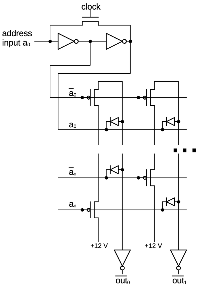
The schematic above shows how the decoder operates. (I've simplified it to two inputs and two outputs.) At the top, the address line goes through a latch formed from two inverters and a pass transistor. The address line and its complement form two row lines; the other row lines are similar. Each column has a transistor on one row line and a diode on the other, selecting the address for that column. For instance, supposed a0 is 1 and an is 0. This matches the first column since the transistor lines are low and the diode lines are high. The PMOS transistors in the column will all turn on, pulling the input to the inverter high. However, if any of the inputs are "wrong", the corresponding transistor will turn off, blocking the +12 volts. Moreover, the output will be pulled low through the corresponding diode. Thus, each column will be pulled high only if all the inputs match, and otherwise it will be pulled low. Each column output controls one of the chip's registers, allowing that register to be accessed.

The HP-IB bus and the PHI chip

The Hewlett-Packard Interface Bus (HP-IB) was designed in the early 1970s as a low-cost bus for connecting diverse devices including instrument systems (such as a digital voltmeter or frequency counter), storage, and computers. This bus became an IEEE standard in 1975, known as the IEEE-488 bus.2 The bus is 8-bits parallel, with handshaking between devices so slow devices can control the speed.

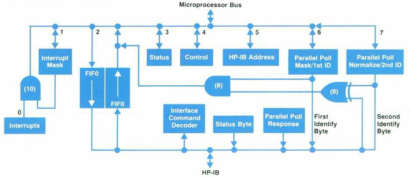
In 1977, HP Developed a chip, known as PHI (Processor to HP-IB Interface) to implement the bus protocol and provide a microprocessor interface. This chip not only simplified construction of a bus controller but also ensured that devices implemented the protocol consistently. The block diagram below shows the components of the PHI chip. It's not an especially complex chip, but it isn't trivial either. I estimate that it has several thousand transistors.

Block diagram from HP Journal, July 1989.

Block diagram from HP Journal, July 1989.

The die photo below shows some of the functional blocks of the PHI chip. The microprocessor connected to the top pins, while the interface bus connected to the lower pins.

The PHI die with some functional blocks labeled,

The PHI die with some functional blocks labeled,

Conclusions

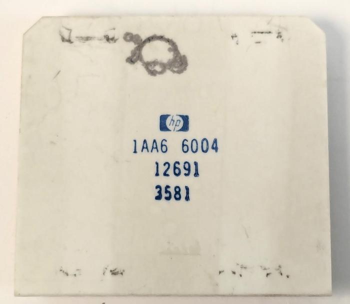
Top of the PHI chip, with the 1AA6-6004 part number. I'm not sure what the oval stamp at the top is, maybe a turtle?

Top of the PHI chip, with the 1AA6-6004 part number. I'm not sure what the oval stamp at the top is, maybe a turtle?

The PHI chip is interesting as an example of a "technology of the future" that didn't quite pan out. HP put a lot of effort into silicon-on-sapphire chips, expecting that this would become an important technology: dense, fast, and low power. However, regular silicon chips turned out to be the winning technology and silicon-on-sapphire was relegated to niche markets.

Comparing HP's silicon-on-sapphire chips to regular silicon chips at the time shows some advantages and disadvantages. HP's MC2 16-bit processor (1977) used silicon-on-sapphire technology and had 10,000 transistors and ran at 8 megahertz, using 350 mW. In comparison, the Intel 8086 (1978) was also a 16-bit processor, but implemented on regular silicon and using NMOS instead of CMOS. The 8086 had 29,000 transistors, ran at 5 megahertz (at first) and used up to 2.5 watts. The sizes of the chips were almost identical: 34 mm2 for the HP processor and 33 mm2 for the Intel processor. This illustrates that CMOS uses much less power than NMOS, one of the reasons that CMOS is now the dominant technology. For the other factors, silicon-on-sapphire had a bit of a speed advantage but wasn't as dense. Silicon-on-sapphire's main problem was its low yield and high cost. Crystal incompatibilities between silicon and sapphire made manufacturing difficult; HP achieved a yield of 9%, meaning 91% of the dies failed.

The time period of the PHI chip is also interesting since interface buses were transitioning from straightforward buses to high-performance buses with complex protocols. Early buses could be implemented with simple integrated circuits, but as protocols became more complex, custom interface chips became necessary. (The MOS 6522 Versatile Interface Adapter chip (1977) is another example, used in many home computers of the 1980s.) But these interfaces were still simple enough that the interface chips didn't require microcontrollers, using simple state machines instead.

The HP logo on the die of the PHI chip.

The HP logo on the die of the PHI chip.

For more, follow me on Twitter @kenshirriff or RSS for updates. I'm also on Mastodon occasionally as @[email protected]. Thanks to CuriousMarc for providing the chip and to TubeTimeUS for help with decapping.

Notes and references

  1. More information: The article What is Silicon-on-Sapphire discusses the history and construction. Details on the HP-IB bus are here. The HP 12009A HP-IB Interface Reference Manual has information on the PHI chip and the protocol. See also the PHI article from HP Journal, July 1989. EvilMonkeyDesignz also shows a decapped PHI chip. 

  2. People with Commodore PET computers may recognize the IEEE-488 bus since peripherals such as floppy disk drives were connected using the IEEE-488 bus. The cables were generally expensive and harder to obtain than interface cables used by other computers. The devices were also slow compared to other computers, although I think this was due to the hardware, not the bus. 

Two interesting XOR circuits inside the Intel 386 processor

Intel's 386 processor (1985) was an important advance in the x86 architecture, not only moving to a 32-bit processor but also switching to a CMOS implementation. I've been reverse-engineering parts of the 386 chip and came across two interesting and completely different circuits that the 386 uses to implement an XOR gate: one uses standard-cell logic while the other uses pass-transistor logic. In this article, I take a look at those circuits.

The die of the 386. Click this image (or any other) for a larger version.

The die of the 386. Click this image (or any other) for a larger version.

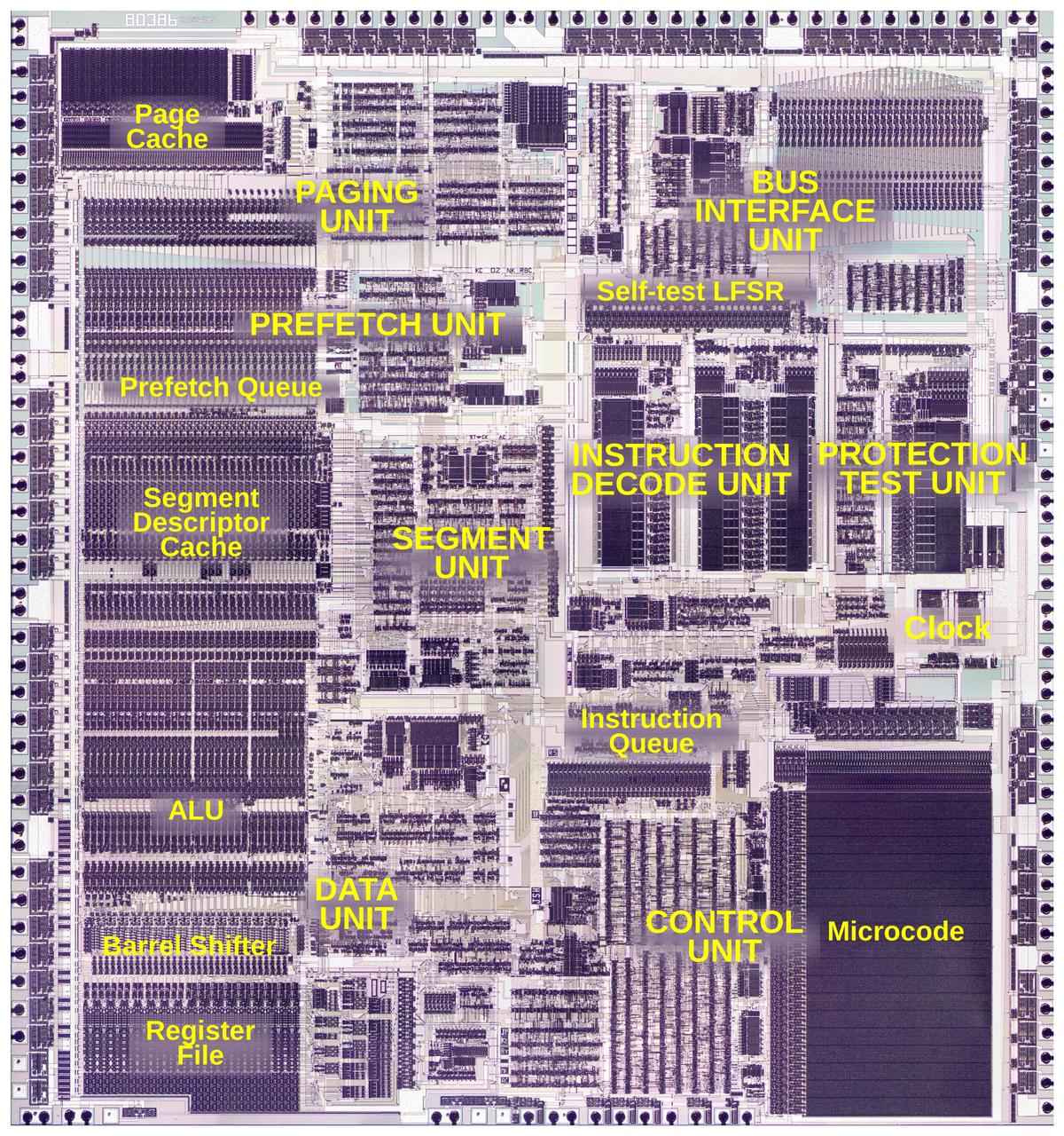
The die photo above shows the two metal layers of the 386 die. The polysilicon and silicon layers underneath are mostly hidden by the metal. The black dots around the edges are the bond wires connecting the die to the external pins. The 386 is a complicated chip with 285,000 transistor sites. I've labeled the main functional blocks. The datapath in the lower left does the actual computations, controlled by the microcode ROM in the lower right.

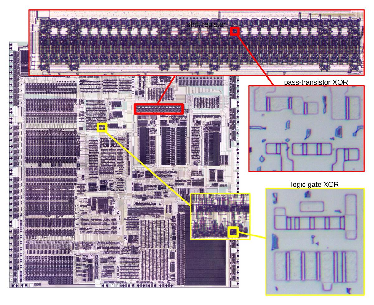
Despite the complexity of the 386, if you zoom in enough, you can see individual XOR gates. The red rectangle at the top (below) is a shift register for the chip's self-test. Zooming in again shows the silicon for an XOR gate implemented with pass transistors. The purple outlines reveal active silicon regions, while the stripes are transistor gates. The yellow rectangle zooms in on part of the standard-cell logic that controls the prefetch queue. The closeup shows the silicon for an XOR gate implemented with two logic gates. Counting the stripes shows that the first XOR gate is implemented with 8 transistors while the second uses 10 transistors. I'll explain below how these transistors are connected to form the XOR gates.

The die of the 386, zooming in on two XOR gates.

The die of the 386, zooming in on two XOR gates.

A brief introduction to CMOS

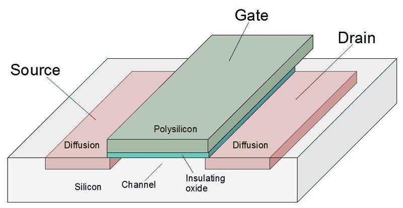
CMOS circuits are used in almost all modern processors. These circuits are built from two types of transistors: NMOS and PMOS. These transistors can be viewed as switches between the source and drain controlled by the gate. A high voltage on the gate of an NMOS transistor turns the transistor on, while a low voltage on the gate of a PMOS transistor turns the transistor on. An NMOS transistor is good at pulling the output low, while a PMOS transistor is good at pulling the output high. Thus, NMOS and PMOS transistors are opposites in many ways; they are complementary, which is the "C" in CMOS.

Structure of a MOS transistor. Although the transistor's name represents the Metal-Oxide-Semiconductor layers, modern MOS transistors typically use polysilicon instead of metal for the gate.

Structure of a MOS transistor. Although the transistor's name represents the Metal-Oxide-Semiconductor layers, modern MOS transistors typically use polysilicon instead of metal for the gate.

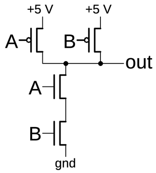
In a CMOS circuit, the NMOS and PMOS transistors work together, with the NMOS transistors pulling the output low as needed while the PMOS transistors pull the output high. By arranging the transistors in different ways, different logic gates can be created. The diagram below shows a NAND gate constructed from two PMOS transistors (top) and two NMOS transistors (bottom). If both inputs are high, the NMOS transistors turn on and pull the output low. But if either input is low, a PMOS transistor will pull the output high. Thus, the circuit below implements a NAND gate.

A NAND gate implemented in CMOS.

A NAND gate implemented in CMOS.

Notice that NMOS and PMOS transistors have an inherent inversion: a high input produces a low (for NMOS) or a low input produces a high (for PMOS). Thus, it is straightforward to produce logic circuits such as an inverter, NAND gate, NOR gate, or an AND-OR-INVERT gate. However, producing an XOR (exclusive-or) gate doesn't work with this approach: an XOR gate produces a 1 if either input is high, but not both.1 The XNOR (exclusive-NOR) gate, the complement of XOR, also has this problem. As a result, chips often have creative implementations of XOR gates.

The standard-cell two-gate XOR circuit

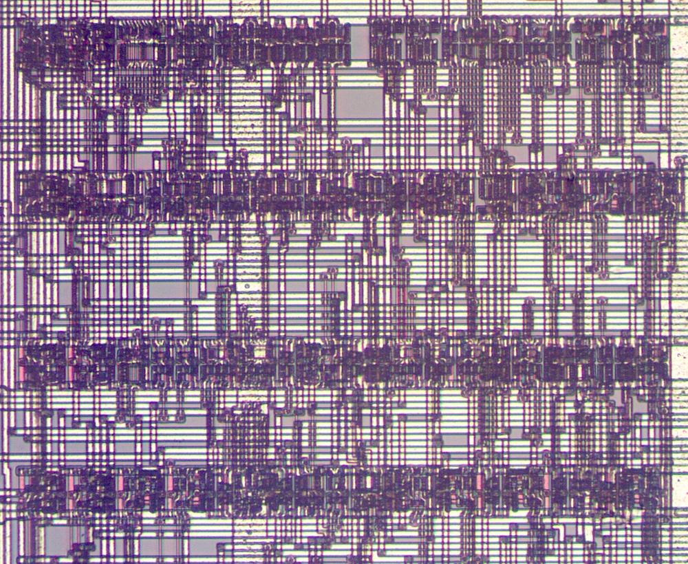
Parts of the 386 were implemented with standard-cell logic. The idea of standard-cell logic is to build circuitry out of standardized building blocks that can be wired by a computer program. In earlier processors such as the 8086, each transistor was carefully positioned by hand to create a chip layout that was as dense as possible. This was a tedious, error-prone process since the transistors were fit together like puzzle pieces. Standard-cell logic is more like building with LEGO. Each gate is implemented as a standardized block and the blocks are arranged in rows, as shown below. The space between the rows holds the wiring that connects the blocks.

Some rows of standard-cell logic in the 386 processor. This is part of the segment descriptor control circuitry.

Some rows of standard-cell logic in the 386 processor. This is part of the segment descriptor control circuitry.

The advantage of standard-cell logic is that it is much faster to create a design since the process can be automated. The engineer described the circuit in terms of the logic gates and their connections. A computer algorithm placed the blocks so related blocks are near each other. An algorithm then routed the circuit, creating the wiring between the blocks. These "place and route" algorithms are challenging since it is an extremely difficult optimization problem, determining the best locations for the blocks and how to pack the wiring as densely as possible. At the time, the algorithm took a day on a powerful IBM mainframe to compute the layout. Nonetheless, the automated process was much faster than manual layout, cutting weeks off the development time for the 386. The downside is that the automated layout is less dense than manually optimized layout, with a lot more wasted space. (As you can see in the photo above, the density is low in the wiring channels.) For this reason, the 386 used manual layout for circuits where a dense layout was important, such as the datapath.

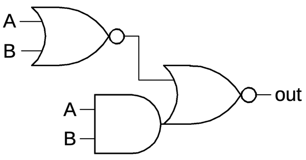
In the 386, the standard-cell XOR gate is built by combining a NOR gate with an AND-NOR gate as shown below.2 (Although AND-NOR looks complicated, it is implemented as a single gate in CMOS.) You can verify that if both inputs are 0, the NOR gate forces the output low, while if both inputs are 1, the AND gate forces the output low, providing the XOR functionality.

Schematic of an XOR circuit.

Schematic of an XOR circuit.

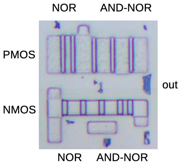
The photo below shows the layout of this XOR gate as a standard cell. I have removed the metal and polysilicon layers to show the underlying silicon. The outlined regions are the active silicon, with PMOS above and NMOS below. The stripes are the transistor gates, normally covered by polysilicon wires. Notice that neighboring transistors are connected by shared silicon; there is no demarcation between the source of one transistor and the drain of the next.

The silicon implementing the XOR standard cell. This image is rotated 180° from the layout on the die to put PMOS at the top.

The silicon implementing the XOR standard cell. This image is rotated 180° from the layout on the die to put PMOS at the top.

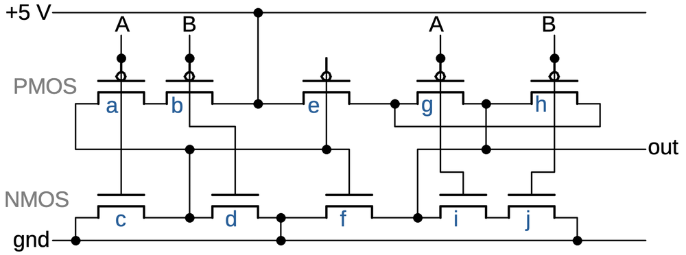
The schematic below corresponds to the silicon above. Transistors a, b, c, and d implement the first NOR gate. Transistors g, h, i, and j implement the AND part of the AND-NOR gate. Transistors e and f implement the NOR input of the AND-NOR gate, fed from the first NOR gate. The standard cell library is designed so all the cells are the same height with a power rail at the top and a ground rail at the bottom. This allows the cells to "snap together" in rows. The wiring inside the cell is implemented in polysilicon and the lower metal layer (M1), while the wiring between cells uses the upper metal layer (M2) for vertical connections and lower metal (M1) for horizontal connections. This strategy allows vertical wires to pass over the cells without interfering with the cell's wiring.

Transistor layout in the XOR standard cell.

Transistor layout in the XOR standard cell.

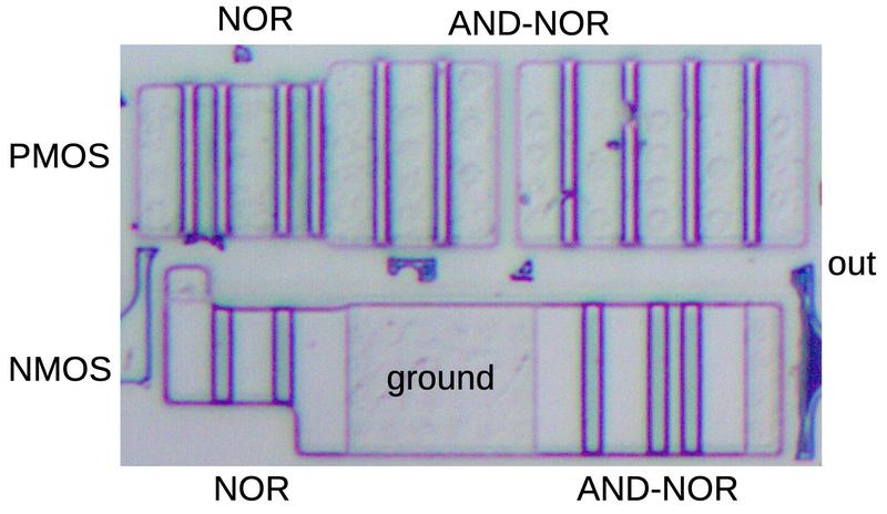
One important factor in a chip such as the 386 is optimizing the sizes of transistors. If a transistor is too small, it will take too much time to switch its output line, reducing performance. But if a transistor is too large, it will waste power as well as slowing down the circuit that is driving it. Thus, the standard-cell library for the 386 includes several XOR gates of various sizes. The diagram below shows a considerably larger XOR standard cell. The cell is the same height as the previous XOR (as required by the standard cell layout), but it is much wider and the transistors inside the cell are taller. Moreover, the PMOS side uses pairs of transistors to double the current capacity. (NMOS has better performance than PMOS so doesn't require doubling of the transistors.) Thus, there are 10 PMOS transistors and 5 NMOS transistors in this XOR cell.

A large XOR standard cell. This cell is also rotated from the die layout.

A large XOR standard cell. This cell is also rotated from the die layout.

The pass transistor circuit

Some parts of the 386 implement XOR gates completely differently, using pass transistor logic. The idea of pass transistor logic is to use transistors as switches that pass inputs through to the output, rather than using transistors as switches to pull the output high or low. The pass transistor XOR circuit uses 8 transistors, compared with 10 for the previous circuit.3

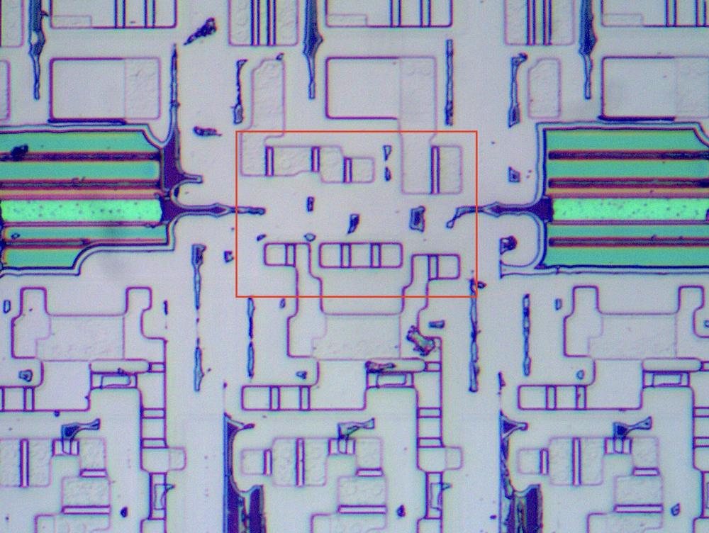
The die photo below shows a pass-transistor XOR circuit, highlighted in red. Note that the surrounding circuitry is irregular and much more tightly packed than the standard-cell circuitry. This circuit was laid out manually producing an optimized layout compared to standard cells. It has four PMOS transistors at the top and four NMOS transistors at the bottom.

The pass-transistor XOR circuit on the die. The green regions are oxide that was not completely removed causing thin-film interference.

The pass-transistor XOR circuit on the die. The green regions are oxide that was not completely removed causing thin-film interference.

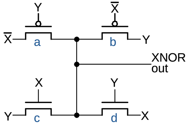
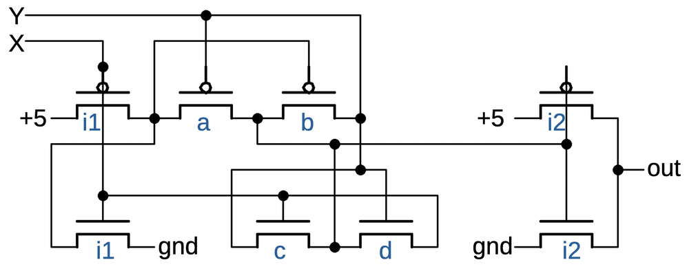
The schematic below shows the heart of the circuit, computing the exclusive-NOR (XNOR) of X and Y with four pass transistors. To understand the circuit, consider the four input cases for X and Y. If X and Y are both 0, PMOS transistor a will turn on (because Y is low), passing 1 to the XNOR output. (X is the complemented value of the X input.) If X and Y are both 1, PMOS transistor b will turn on (because X is low), passing 1. If X and Y are 1 and 0 respectively, NMOS transistor c will turn on (because X is high), passing 0. If X and Y are 0 and 1 respectively, transistor d will turn on (because Y is high), passing 0. Thus, the four transistors implement the XNOR function, with a 1 output if both inputs are the same.

Partial implementation of XNOR with four pass transistors.

Partial implementation of XNOR with four pass transistors.

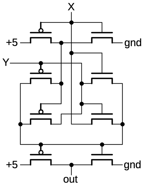
To make an XOR gate out of this requires two additional inverters. The first inverter produces X from X. The second inverter generates the XOR output by inverting the XNOR output. The output inverter also has the important function of buffering the output since the pass transistor output is weaker than the inputs. Since each inverter takes two transistors, the complete XOR circuit uses 8 transistors. The schematic below shows the full circuit. The i1 transistors implement the input inverter and the i2 transistors implement the output inverter. The layout of this schematic matches the earlier die photo.5

Implementation of NOR with eight pass transistors.

Implementation of NOR with eight pass transistors.

Conclusions

An XOR gate may seem like a trivial circuit, but there is more going on than you might expect. I think it is interesting that there isn't a single solution for implementing XOR; even inside a single chip, multiple approaches can be used. (If you're interested in XOR circuits, I also looked at the XOR circuit in the Z80.) It's also reassuring to see that even for a complex chip such as the 386, the circuitry can be broken down into logic gates and then understood at the transistor level.

I plan to write more about the 386, so follow me on Twitter @kenshirriff or RSS for updates. I'm also on Mastodon occasionally as @[email protected].

Notes and references

  1. You can't create an AND or OR gate directly from CMOS either, but this isn't usually a problem. One approach is to create a NAND (or NOR) gate and then follow it with an inverter, but this requires an "extra" inverter. However, the inverter can often be eliminated by flipping the action of the next gate (using De Morgan's laws). For example, if you have AND gates feeding into an OR gate, you can change the circuit to use NAND gates feeding into a NAND gate, eliminating the inverters. Unfortunately, flipping the logic levels doesn't help with XOR gates, since XNOR is just as hard to produce. 

  2. The 386 also uses XNOR standard-cell gates. These are implemented with the "opposite" circuit from XOR, swapping the AND and OR gates:

    Schematic of an XNOR circuit.

    Schematic of an XNOR circuit.


  3. I'm not sure why some circuits in the 386 use standard logic for XOR while other circuits use pass transistor logic. I suspect that the standard XOR is used when the XOR gate is part of a standard-cell logic circuit, while the pass transistor XOR is used in hand-optimized circuits. There may also be performance advantages to one over the other. 

  4. The first inverter can be omitted in the pass transistor XOR circuit if the inverted input happens to be available. In particular, if multiple XOR gates use the same input, one inverter can provide the inverted input to all of them, reducing the per-gate transistor count. 

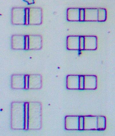
  5. The pass transistor XOR circuit uses different layouts in different parts of the 386, probably because hand layout allows it to be optimized. For instance, the instruction decoder uses the XOR circuit below. This circuit has four PMOS transistors on the left and four NMOS transistors on the right.

    An XOR circuit from the instruction decoder.

    An XOR circuit from the instruction decoder.

    The schematic shows the wiring of this circuit. Although the circuit is electrically the same as the previous pass-transistor circuit, the layout is different. In the previous circuit, several of the transistors were connected through their silicon, while this circuit has all the transistors separated and arranged in columns.

    Schematic of the XOR circuit from the instruction decoder.

    Schematic of the XOR circuit from the instruction decoder.


Reverse engineering the barrel shifter circuit on the Intel 386 processor die

The Intel 386 processor (1985) was a large step from the 286 processor, moving x86 to a 32-bit architecture. The 386 also dramatically improved the performance of shift and rotate operations by adding a "barrel shifter", a circuit that can shift by multiple bits in one step. The die photo below shows the 386's barrel shifter, highlighted in the lower left and taking up a substantial part of the die.
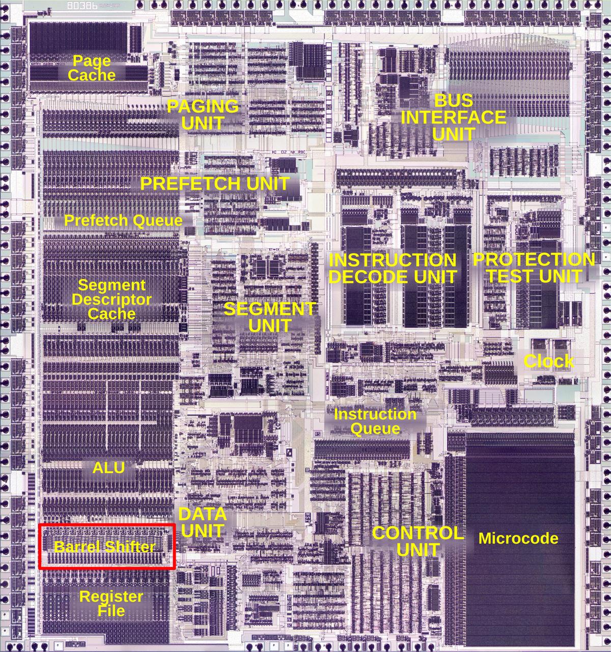
The 386 die with the main functional blocks labeled. Click this image (or any other) for a larger version.)

The 386 die with the main functional blocks labeled. Click this image (or any other) for a larger version.)

Shifting is a useful operation for computers, moving a binary value left or right by one or more bits. Shift instructions can be used for multiplying or dividing by powers of two, and as part of more general multiplication or division. Shifting is also useful for extracting bit fields, aligning bitmap graphics, and many other tasks.1

Barrel shifters require a significant amount of circuitry. A common approach is to use a crossbar, a matrix of switches that can connect any input to any output. By closing switches along a desired diagonal, the input bits are shifted. The diagram below illustrates a 4-bit crossbar barrel shifter with inputs X (vertical) and outputs Y (horizontal). At each point in the grid, a switch (triangle) connects a vertical input line to a horizontal output line. Energizing the blue control line, for instance, passes the value through unchanged (X0 to Y0 and so forth). Energizing the green control line rotates the value by one bit position (X0 to Y1 and so forth, with X3 wrapping around to X0). Similarly, the circuit can shift by 2 or 3 bits. The shift control lines select the amount of shift. These lines run diagonally, which will be important later.
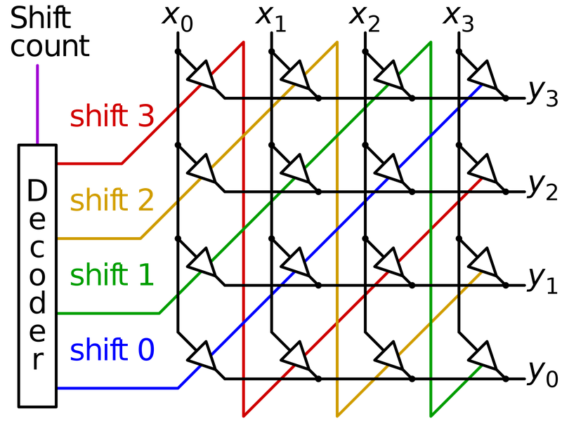
A four-bit crossbar switch with inputs X and outputs Y. Image by Cmglee, CC BY-SA 3.0.

A four-bit crossbar switch with inputs X and outputs Y. Image by Cmglee, CC BY-SA 3.0.

The main problem with a crossbar barrel shifter is that it takes a lot of hardware. The 386's barrel shifter has a 64-bit input and a 32-bit output,2 so the approach above would require 2048 switches (64×32). For this reason, the 386 uses a hybrid approach, as shown below. It has a 32×8 crossbar that can shift by 0 to 28 bits, but only in multiples of 4, making the circuit much smaller. The output from the crossbar goes to a second circuit that can shift by 0, 1, 2, or 3 bits. The combined circuitry supports an arbitrary shift, but requires less hardware than a complete crossbar. The inputs to the barrel shifter are two 32-bit values from the processor's register file, stored in latches for use by the shifter.
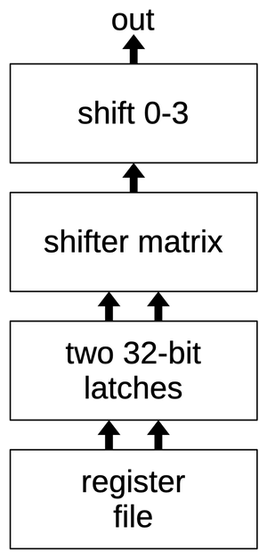
Block diagram of the barrel shifter circuit.

Block diagram of the barrel shifter circuit.

The figure below shows how the shifter circuitry appears on the die; this image shows the two metal layers on the die's surface. The inputs from the register file are at the bottom, for bits 31 through 0. Above that, the input latches hold the two 32-bit inputs for the shifter. In the middle is the heart of the shift circuit, the crossbar matrix. This takes the two 32-bit inputs and produces a 32-bit output. The matrix is controlled by sloping polysilicon lines, driven by control circuitry on the right. The matrix output goes to the circuit that applies a shift of 0 to 3 positions. Finally, the outputs exit at the top, where they go to other parts of the CPU. The shifter performs right shifts, but as will be explained below, the same circuit is used for the left shift instructions.
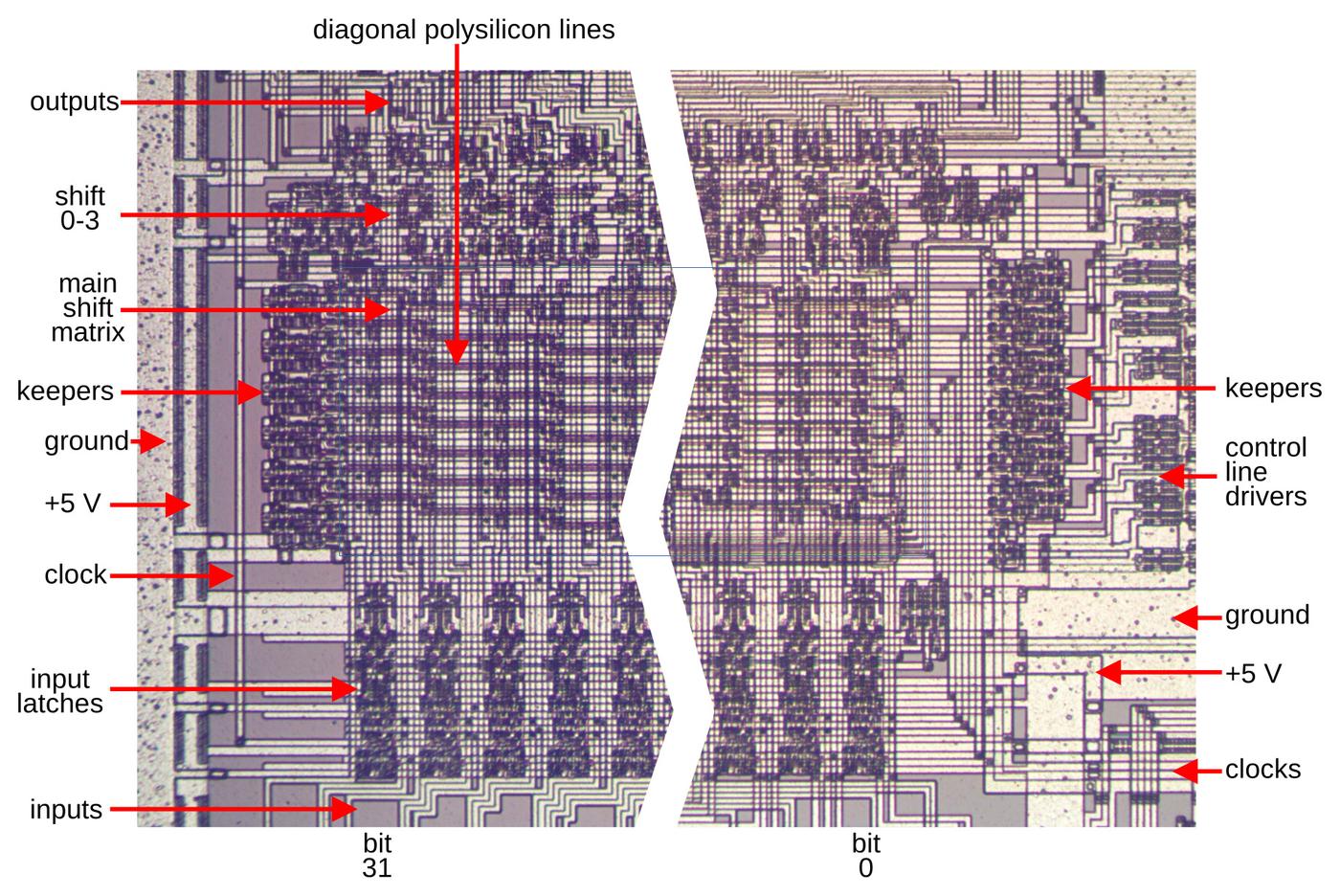
The barrel shifter circuitry as it appears on the die. I have cut out repetitive circuitry from the middle because the complete image is too wide to display clearly.

The barrel shifter circuitry as it appears on the die. I have cut out repetitive circuitry from the middle because the complete image is too wide to display clearly.

The barrel shifter crossbar matrix

In this section, I'll describe the matrix part of the barrel shifter circuit. The shift matrix takes 32-bit values a and b. Value b is shifted to the right, with bits from a filling in at the left, producing a 32-bit output. (As will be explained below, the output is actually 37 bits due to some complications, but ignore that for now.) The shift count is a multiple of 4 from 0 to 28.

The diagram below illustrates the structure of the shift matrix. The two 32-bit inputs are provided at the bottom, interleaved, and run vertically. The 32 output lines run horizontally. The 8 control lines run diagonally, activating the switches (black dots) to connect inputs and outputs. (For simplicity, only 3 control lines are shown.) For a shift of 0, control line 0 (red) is selected and the output is b31b30...b1b0. (You can verify this by matching up inputs to outputs through the dots along the red line.)
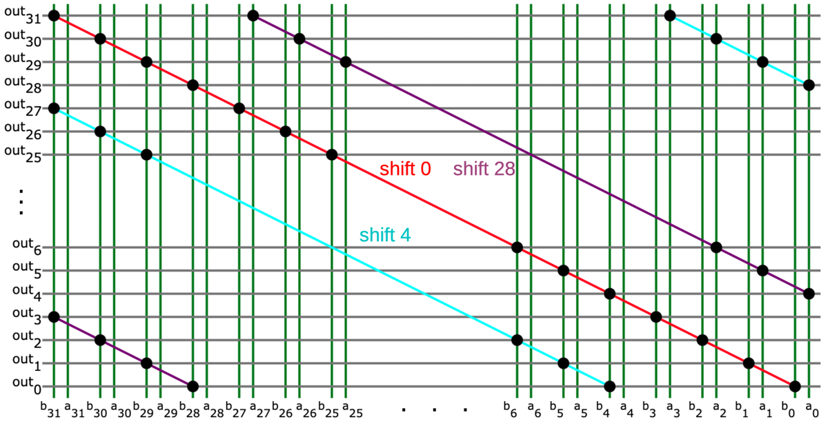
Diagram of the shift matrix, showing three of the shift control lines.

Diagram of the shift matrix, showing three of the shift control lines.

For a shift right of 4, the cyan control line is activated. It can be seen that the output in this case is a3a2a1a0b31b30...b5b4, shifting b to the right 4 bits and filling in four bits from a as desired. For a shift of 28, the purple control line is activated, producing the output a27...a0b31...b28. Note that the control lines are spaced four bits apart, which is why the matrix only shifts by a multiple of 4. Another important feature is that below the red diagonal, the b inputs are connected to the output, while above the diagonal, the a inputs are connected to the output. (In other words, the black dots are shifted to the right above the diagonal.) This implements the 64-bit support, taking bits from a or b as appropriate.

Looking at the implementation on the die, the vertical wires use the lower metal layer (metal 1) while the horizontal wires use the upper metal layer (metal 2), so the wires don't intersect. NMOS transistors are used as the switches to connect inputs and outputs.4 The transistors are controlled by diagonal wires constructed of polysilicon that form the transistor gates. When a particular polysilicon wire is energized, it turns on the transistors along a diagonal line, connecting those inputs and outputs.

The image below shows the left side of the matrix.5 The polysilicon control lines are the green horizontal lines stepping down to the right. These control the transistors, which appear as columns of blue-gray squares next to the polysilicon lines. The metal layers have been removed; the position of the lower metal 1 layer is visible in the vertical bluish lines.
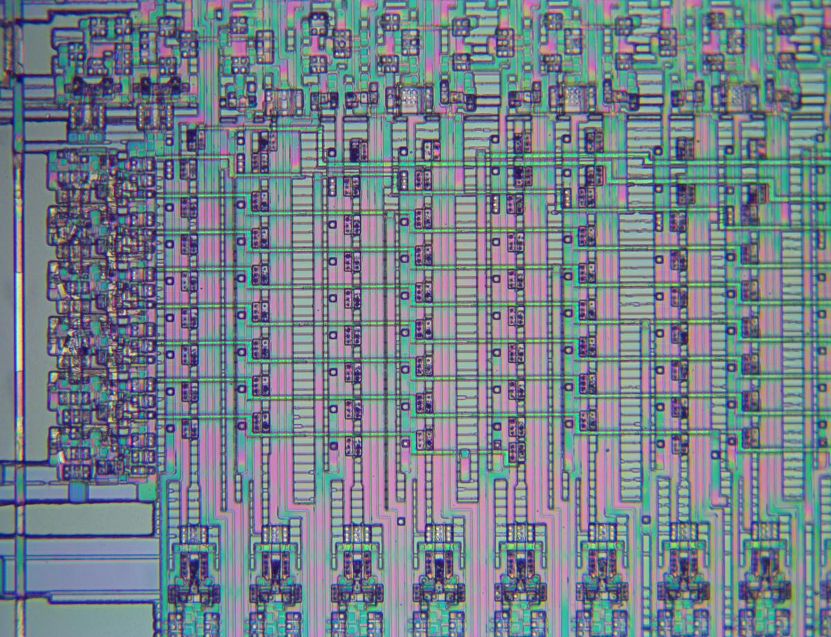
The left side of the matrix as it appears on the die.

The left side of the matrix as it appears on the die.

The diagram below shows four of these transistors in the shifter matrix. There are four circuitry layers involved. The underlying silicon is pinkish gray; the active regions are the squares with darker borders. Next is the polysilicon (green), which forms the control lines and the transistor gates. The lower metal layer (metal 1) forms the blue vertical lines that connect to the transistors.3 The upper metal layer (metal 2) forms the horizontal bit output lines. Finally, the small black dots are the vias that connect metal 1 and metal 2. (The well taps are silicon regions connected to ground to prevent latch-up.)
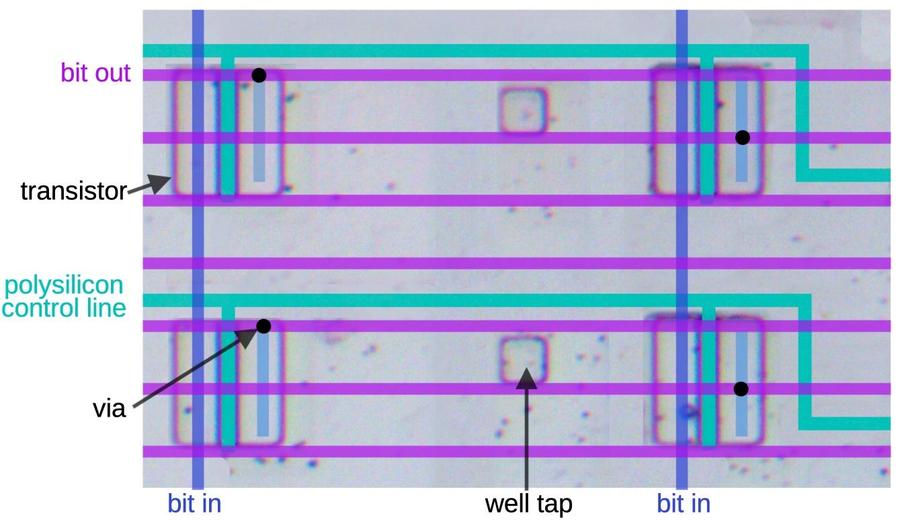
Four transistors in the shifter matrix. The polysilicon and metal lines have been drawn in.

Four transistors in the shifter matrix. The polysilicon and metal lines have been drawn in.

To see how this works, suppose the upper polysilicon line is activated, turning on the top two transistors. The two vertical bit-in lines (blue) will be connected through the transistors to the top two bit out lines (purple), by way of the short light blue metal segments and the via (black dot). However, if the lower polysilicon line is activated, the bottom two transistors will be turned on. This will connect the bit-in lines to the fifth and sixth bit-out lines, four lines down from the previous ones. Thus, successive polysilicon lines shift the connections down by four lines at a time, so the shifts change in steps of 4 bit positions.

As mentioned earlier, to support the 64-bit input, the transistors below the diagonal are connected to b input while the transistors above the diagonal are connected to the a input. The photo below shows the physical implementation: the four upper transistors are shifted to the right by one wire width, so they connect to vertical a wires, while the four lower transistors are connected to b wires. (The metal wires were removed for this photo to show the transistors.)
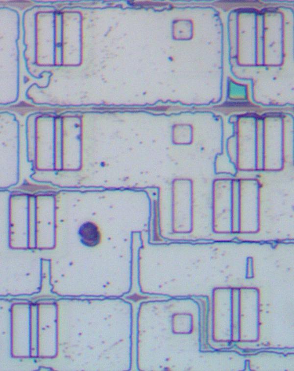
This photo of the underlying silicon shows eight transistors. The top four transistors are shifted one position to the right. the irregular lines are remnants of other layers that I couldn't completely remove from the die.

This photo of the underlying silicon shows eight transistors. The top four transistors are shifted one position to the right. the irregular lines are remnants of other layers that I couldn't completely remove from the die.

In the matrix, the output signals run horizontally. In order for signals to exit the shifter from the top of the matrix, each horizontal output wire is connected to a vertical output wire. Meanwhile, other processor signals (such as the register write data) must also pass vertically through the shifter region. The result is a complicated layout, packing everything together as tightly as possible.

The precharge/keepers

At the left and the right of the barrel shifter, repeated blocks of circuitry are visible. These blocks contain precharge and keeper circuits to hold the value on one of the lines. During the first clock phase, each horizontal bit line is precharged to +5 volts. Next, the matrix is activated and horizontal lines may be pulled low. If the line is not pulled low, the inverter and PMOS transistor will continuously pull the line high. The inverter and transistor can be viewed as a bus keeper, essentially a weak latch to hold the line in the 1 state. The keeper uses relatively weak transistors, so the line can be pulled low when the barrel shifter is activated. The purpose of the keeper is to ensure that the line doesn't drift into a state between 0 and 1. This is a bad situation with CMOS circuitry, since the pull-up and pull-down transistors could both turn on, yielding a short circuit.
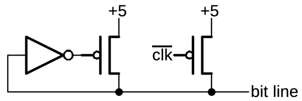
The precharge/keeper circuit

The precharge/keeper circuit

The motivation behind this design is that implementing the matrix with "real" CMOS would require twice as many transistors. By implementing the matrix with NMOS transistors only, the size is reduced. In a standard NMOS implementation, pull-up transistors would continuously pull the lines high, but this results in fairly high power consumption. Instead, the precharge circuit pulls the line high at the start. But this results in dynamic logic, dependent on the capacitance of the circuit to hold the charge. To avoid the charge leaking away, the keeper circuit keeps the line high until it is pulled low. Thus, this circuit minimizes the area of the matrix as well as minimizing power consumption.

There are 37 keepers in total for the 37 output lines from the matrix.6 (The extra 5 lines will be explained below.) The photo below shows one block of three keepers; the metal has been removed to show the silicon transistors and some of the polysilicon (green).
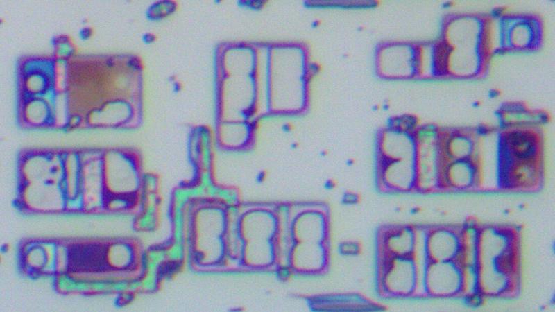
One block of keeper circuitry, to the right of the shift matrix. This block has 12 transistors, supporting three bits.

One block of keeper circuitry, to the right of the shift matrix. This block has 12 transistors, supporting three bits.

The register latches

At the bottom of the shift circuit, two latches hold the two 32-bit input values. The 386 has multi-ported registers, so it can access two registers and write a third register at the same time. This allows the shift circuit to load both values at the same time. I believe that a value can also come from the 386's constant ROM, which is useful for providing 0, 1, or all-ones to the shifter.

The schematic below shows the register latches for one bit of the shifter. Starting at the bottom are the two inputs from the register file (one appears to be inverted for no good reason). Each input is stored in a latch, using the standard 386 latch circuit.7 The latched input is gated by the clock and then goes through multiplexers allowing either value to be used as either input to the shifter. (The shifter takes two 32-bit inputs and this multiplexer allows the inputs to be swapped to the other sides of the shifter.) A second latch stage holds the values for the output; this latch is cleared during the first clock phase and holds the desired value during the second clock phase.
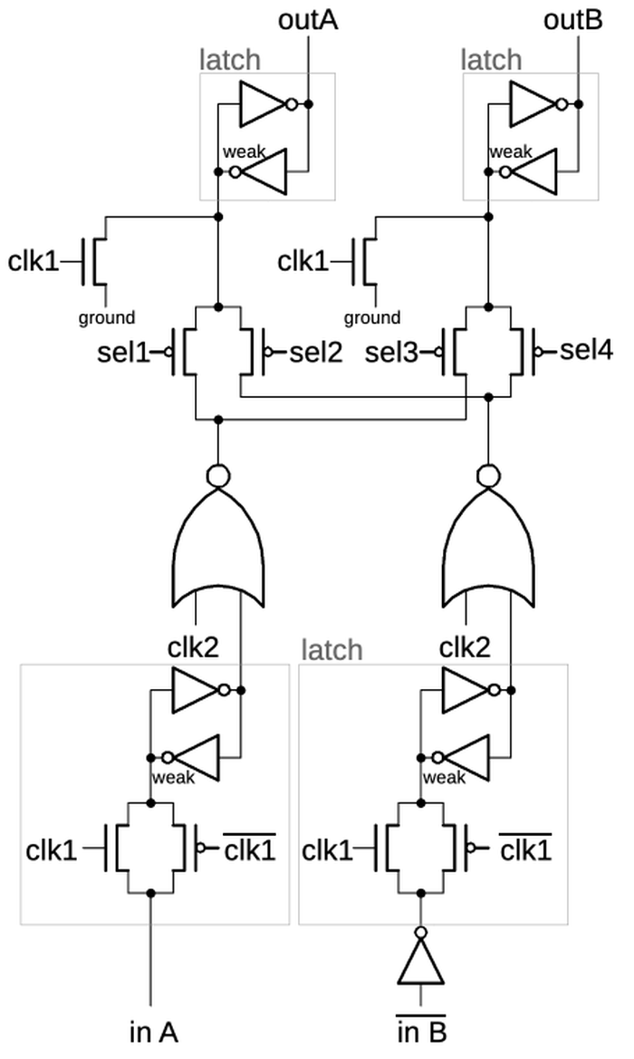
Circuit for one bit of the register latch.

Circuit for one bit of the register latch.

The die photo below shows the register latch circuit, contrasting the metal layers (left) with the silicon layer (right). The dark spots in the metal image are vias between the metal layers or connections to the underlying silicon or polysilicon. The metal layer is very dense with vertical wiring in the lower metal 1 layer and horizontal wiring in the upper metal 2 layer. The density of the chip seems to be constrained by the metal wiring more than the density of the transistors.
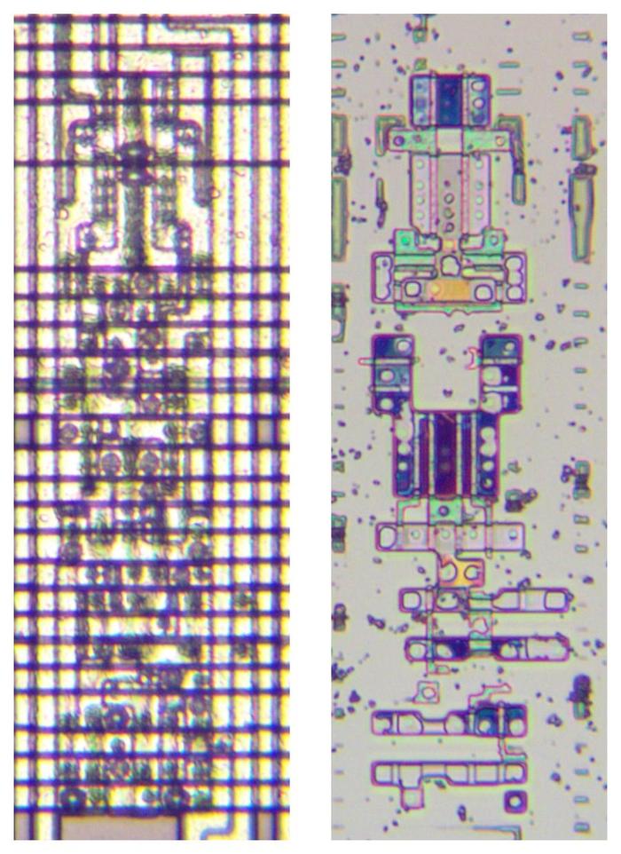
One of the register latch circuits.

One of the register latch circuits.

The 0-3 shifter

The shift matrix can only shift in steps of 4 bits. To support other shifts, a circuit at the top of the shifter provides a shift of 0 to 3 bits. In conjunction, these circuits permit a shift by an arbitrary amount.8 The schematic below shows the circuit. A bit enters at the bottom. The first shift stage passes the bit through, or sends it one bit position to the right. The second stage passes the bit through, or sends it two bit positions to the right. Thus, depending on the control lines, each bit can be shifted by 0 to 3 positions to the right. At the top, a transistor pulls the circuit low to initialize it; the NOR gate at the bottom does the same. A keeper transistor holds the circuit low until a data bit pulls it high.
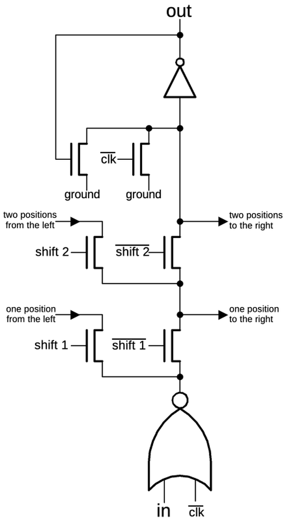
One bit of the 0-3 shifter circuit.

One bit of the 0-3 shifter circuit.

The diagram below shows the silicon implementation corresponding to two copies of the schematic above. The shifters are implemented in pairs to slightly optimize the layout. In particular, the two NOR gates are mirrored so the power connection can be shared. This is a small optimization, but it illustrates that the 386 designers put a lot of work into making the layout dense.
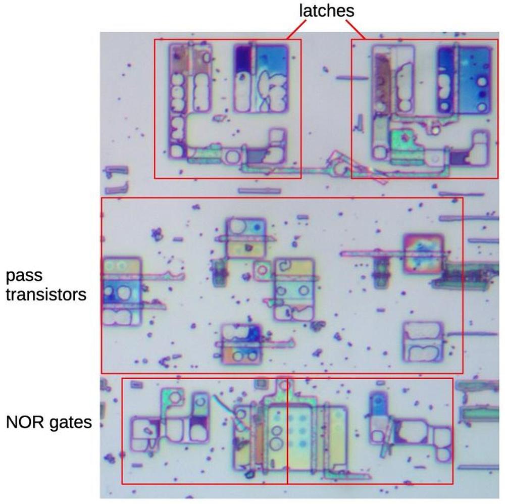
Two bits of the 0-3 shifter circuit as it appears on the die.

Two bits of the 0-3 shifter circuit as it appears on the die.

Complications

As is usually the case with x86, there are a few complications. One complication is that the shift matrix has 37 outputs, rather than the expected 32. There are two reasons behind this. First, the upper shifter will shift right by up to 3 positions, so it needs 3 extra bits. Thus, the matrix needs to output bits 0 through 34 so three bits can be discarded. Second, shift instructions usually produce a carry bit from the last bit shifted out of the word. To support this, the shift matrix provides an extra bit at both ends for use as the carry. The result is that the matrix produces 37 outputs, which can be viewed as bits -1 through 35.

Another complication is that the x86 instruction set supports shifts on bytes and 16-bit words as well as 32-bit words. If you put two 8-bit bytes into the shifter, there will be 24 unused bits in between, posing a problem for the shifter. The solution is that some of the diagonal control lines in the matrix are split on byte and word boundaries, allowing an 8- or 16-bit value to be shifted independently. For example, you can perform a 4-bit right shift on the right-hand byte, and a 28-bit right shift on the left-hand byte. This brings the two bytes together in the result, yielding the desired 4-bit right shift. As a result, there are 18 diagonal control lines in the shifter (if I counted correctly), rather than the expected 8 control lines. This makes the circuitry to drive the control lines more complicated, as it must generate different signals depending on the size of the operand.

The control circuitry

The control circuitry at the right of the shifter drives the diagonal polysilicon lines in the matrix, selecting the desired shift. It also generates control signals for the 0-3 shifter, selecting a shift-by-1 or shift-by-2 as necessary. This circuitry operates under the control of the microcode, which tells it when to shift. It gets the shift amount from the instruction or the CL register and generates the appropriate control signals.

The distribution of control signals is more complex than you might expect. If possible, the polysilicon diagonals are connected on the right of the matrix to the control circuitry, providing a direct connection. However, many of the diagonals do not extend all the way to the right, either because they start on the left or because they are segmented for 8- or 16-bit values. Some of these signals are transmitted through polysilicon lines that run underneath the matrix. Others are transmitted through horizontal metal lines that run through the register latches. (These latches don't use many horizontal lines, so there is available space to route other signals.) These signals then ascend through the matrix at various points to connect with the polysilicon lines. This shows that the routing of this circuitry is carefully optimized to make it as compact as possible. Moreover, these "extra" lines disrupt the layout; the matrix is almost a regular pattern, but it has small irregularities throughout.

Implementing x86 shifts and rotates with the barrel shifter

The x86 has a variety of shift and rotate instructions.9 It is interesting to consider how they are implemented using the barrel shifter, since it is not always obvious. In this section, I'll discuss the instructions supported by the 386.

One important principle is that even though the circuitry shifts to the right, by changing the inputs this can achieve a shift to the left. To make this concrete, consider two input words a and b, with the shifter extracting the portion in red below. (I'll use 8-bit examples instead of 32-bit here and below to keep the size manageable.) The circuit shifts b to the right five bits, inserting bits from a at the left. Alternatively, the result can be viewed as shifting a to the left three bits, inserting bits from b at the right. Thus, the same result can be viewed as a right shift of b or a left shift of a. This holds in general, with a 32-bit right shift by N bits equivalent to a left shift by 32-N bits, depending on which word10 you focus on.

a7a6a5a4a3a2a1a0b7b6b5b4b3b2b1b0

Double shifts

The double-shift instructions (Shift Left Double (SHLD) and Shift Right Double (SHRD)) were new in the 386, shifting two 32-bit values to produce a 32-bit result. The last bit shifted out goes into the carry flag (CF). These instructions map directly onto the behavior of the barrel shifter, so I'll start with them.
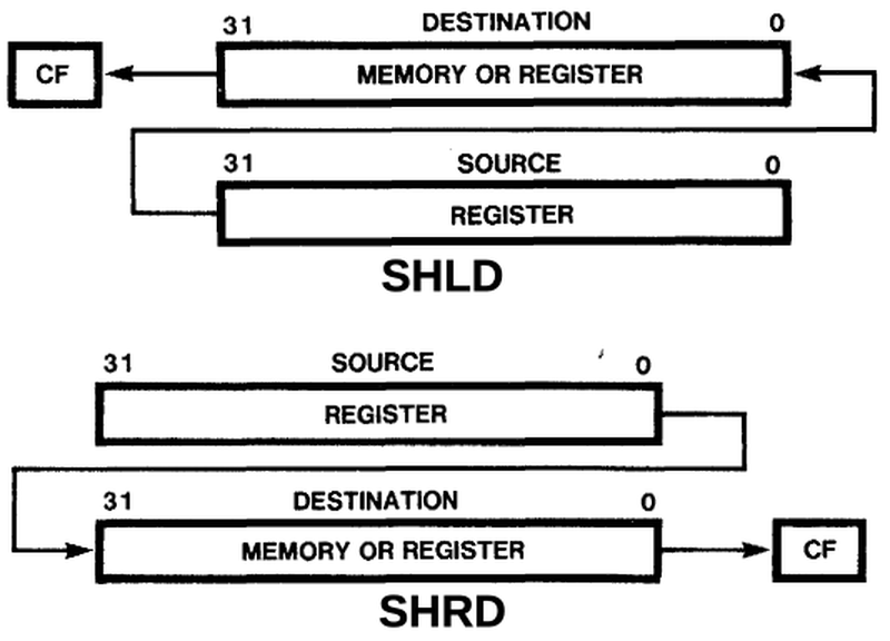
Actions of the double shift instructions.

Actions of the double shift instructions.

The examples below show how the shifter implements the SHLD and SHRD instructions; the shifter output is highlighted in red. (These examples use an 8-bit source (s) and destination (d) to keep them manageable.) In either case, 3 bits of the source are shifted into the destination; shifting left or right is just a matter of whether the destination is on the left or right.

SHLD 3: ddddddddssssssss

SHRD 3: ssssssssdddddddd

Shifts

The basic shift instructions are probably the simplest. Shift Arithmetic Left (SAL) and Shift Logical Left (SHL) are synonyms, shifting the destination to the left and filling with zeroes. This can be accomplished by performing a shift with the word on the left and zeroes on the right. Shift Logical Right (SHR) is the opposite, shifting to the right and filling with zeros. This can be accomplished by putting the word on the right and zeroes on the left. Shift Arithmetic Right (SAR) is a bit different. It fills with the sign bit, the top bit. The purpose of this is to shift a signed number while preserving its sign. It can be implemented by putting all zeroes or all ones on the left, depending on the sign bit. Thus, the shift instructions map nicely onto the barrel shifter.
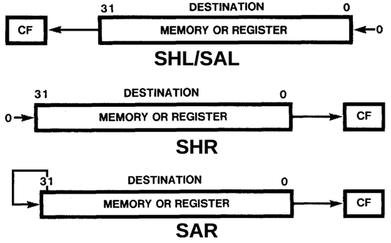
Actions of the shift instructions.

Actions of the shift instructions.

The 8-bit examples below show how the shifter accomplishes the SHL, SHR, and SAR instructions. The destination value d is loaded into one half of the shifter. For SAR, the value's sign bit s is loaded into the other half of the shifter, while the other instructions load 0 into the other half of the shifter. The red box shows the output from the shifter, selected from the input.

SHL 3: dddddddd00000000

SHR 3: 00000000dddddddd

SAR 3: ssssssssdddddddd

Rotates

Unlike the shift instructions, the rotate instructions preserve all the bits. As bits shift off one end, they fill in the other end, so the bit sequence rotates. A rotate left or right is implemented by putting the same word on the left and right.
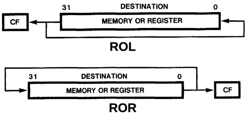
Actions of the rotate instructions.

Actions of the rotate instructions.

The shifter implements rotates as shown below, using the destination value as both shifter inputs. A left shift by N bits is implemented by shifting right by 32-N bits.

ROL 3: d7d6d5d4d3d2d1d0d7d6d5d4d3d2d1d0

ROR 3: d7d6d5d4d3d2d1d0d7d6d5d4d3d2d1d0

Rotates through carry

The rotate through carry instructions perform 33-bit rotates, rotating the value through the carry bit. You might wonder how the barrel shifter can perform a 33-bit rotate, and the answer is that it can't. Instead, the instruction takes multiple steps. If you look at the instruction timings, the other shifts and rotates take three clock cycles. Rotating through the carry, however, takes nine clock cycles, performing multiple steps under the control of the microcode.
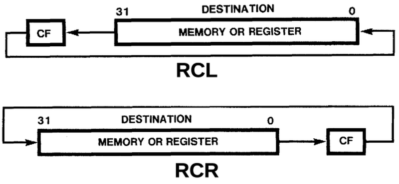
Actions of the rotate through carry instructions.

Actions of the rotate through carry instructions.

Without looking at the microcode, I can only speculate how it takes place. One sequence would be to get the top bits by putting zeroes in the right 32 bits and shifting. Next, get the bottom bits by putting the carry bit in the left 32 bits and shifting one bit more. (That is, set the left 32-bit input to either the constant 0 or 1, depending on the carry.) Finally, the result can be generated by ORing the two shift values together. The example below shows how an RCL 3 could be implemented. In the second step, the carry value C is loaded into the left side of the shifter, so it can get into the result. Note that bit d5 ends up in the carry bit, rather than the result. The RCR instruction would be similar, but adjusting the shift parameters accordingly.

First shift: d7d6d5d4d3d2d1d000000000

Second shift: 0000000Cd7d6d5d4d3d2d1d0

Result from OR: d4d3d2d1d0Cd7d6

Conclusions

The shifter circuit illustrates how the rapidly increasing transistor counts in the 1980s allowed new features. Programming languages make it easy to shift numbers with an expression such as a>>5. But it takes a lot of hardware in the processor to perform these shifts efficiently. The additional hardware of the 386's barrel shifter dramaticallly improved shift performance for shifts and rotates compared to earlier x86 processors. I estimate that the barrel shifter requires about 2000 transistors, about half the number of the entire 6502 processor (1975). But by 1985, putting 2000 transistors into a feature was practical. (In total, the 386 contains 285,000 transistors, a trivial number now, but a large number for the time.)

I plan to write more about the 386, so follow me on Twitter @kenshirriff or RSS for updates. I'm also on Mastodon occasionally as @[email protected].

Notes and references
  1. The earliest reference for a barrel shifter is often given as "A barrel switch design", Computer Design, 1972, but the idea of a barrel shifter goes back to 1964 at least. (The "barrel switch" name presumably comes from a physical barrel switch, a cylindrical multi-position switch such as a car ignition.) The CDC 6600 supercomputer (1964) had a 6-stage shifter able to shift up to 63 positions in one cycle (details); it was called a "parallel shifting network" rather than a "barrel shifter". A Burroughs patent filed in 1965 describes a barrel switch "capable of performing logical switching operations in a single time involving any amount of binary information," so the technology is older.
    Early microprocessors shifted by one bit position at a time. Although the Intel 8086 provided instructions to shift by multiple bits at a time, this was implemented internally by a microcode loop, so the more bits you shifted, the longer the instruction took, four clock cycles per bit. Shifting on the 286 was faster, taking one additional cycle for each bit position shifted. The first ARM processor (ARM1, 1985) included a 32-bit barrel shifter. It was considerably simpler than the 386's design, following ARM's RISC philosophy. 

  2. The 386 Hardware Reference Manual states that the 386 contains a 64-bit barrel shifter. I find this description a bit inaccurate, since the output is only 32 bits, so the barrel shifter is much simpler than a full 64-bit barrel shifter. 

  3. The 386 has two layers of metal. The vertical lines are in the lower layer of metal (metal 1) while the horizontal lines are in the upper layer of metal (metal 2). Transistors can only connect to lower metal, so the connection between the horizontal line and the transistor uses a short piece of lower metal to bridge the layers. 

  4. Each row of the matrix can be considered a multiplexer with 8 inputs, implemented by 8 pass transistors. One of the eight transistors is activated, passing that input to the output. 

  5. The image below shows the full shift matrix. Click the image for a much larger view.

    The matrix with the metal layer removed.

    The matrix with the metal layer removed.


  6. The keepers are arranged with 6 blocks of three on the left and 6 blocks of 3 on the right, plus an additional one at the bottom right. 

  7. The standard latch in the 386 consists of two cross-coupled inverters forming a static circuit to hold a bit. The input goes through a transmission gate (back-to-back NMOS and PMOS transistors) to the inverters. One inverter is weak, so it can be overpowered by the input. The 8086, in contrast, uses dynamic latches that depend on the gate capacitance to hold a bit. 

  8. Some shifters take the idea of combining shift circuits to the extreme. If you combine a shift-by-one circuit, a shift-by-two circuit, a shift-by-four circuit, and so forth, you end up with a logarithmic shifter: selecting the appropriate stages provide an arbitrary shift. (This design was used in the CDC 6600.) This design has the advantage of reducing the amount of circuitry since it uses log2(N) layers rather than N layers. However, the logarithmic approach has performance disadvantages since the signals need to go through more circuitry. This paper describes various design alternatives for barrel shifters. 

  9. The basic rotate left and right instructions date back to the Datapoint 2200, the ancestor of the 8086 and x86. The rotate left through carry and rotate right through carry instructions in x86 were added in the Intel 8008 processor and the 8080 was the same. The MOS 6502 had a different set of rotates and shifts: arithmetic shift left, rotate left, logical shift right, and rotate right; the rotate instructions rotated through the carry. The Z-80 had a more extensive set: rotates left and right, either through the carry or not, shift left, shift right logical, shift right arithmetic, and 4-bit digit rotates left and right through two bytes. The 8086's set of rotates and shifts was similar to the Z-80, except it didn't have the digit rotates. The 8086 also supported shifting and rotating by multiple positions. This illustrates that there isn't a "natural" set of shift and rotate instructions. Instead, different processors supported different instructions, with complexity generally increasing over time. 

  10. The x86 uses "word" to refer to a 16-bit value and "double word" or "dword" to refer to a 32-bit value. I'm going to ignore the word/dword distinction.