Inside the Intel 8087 chip: floating-point addition and subtraction

In 1980, Intel introduced the 8087, a chip that made floating-point operations much faster in the IBM PC and other systems. Although the 8087 supports advanced operations such as tangents, square roots, and logarithms, this article focuses on basic arithmetic operations: addition and subtraction. The 8087 provided a spectacular speed improvement over the 8086 processor, speeding up addition by a factor of almost 100, and complicated operations by even more.1 In this article, I examine the 8087's microcode and circuitry to explain exactly how floating-point addition and subtraction are implemented, including numerous special cases for infinities and other special values.

To explore the 8087's circuitry, I popped the lid off a chip with a chisel and used a microscope to create the high-resolution image below. The microcode ROM is the large rectangular region in the center of the die, holding the 1648 micro-instructions that control the chip. The bottom half of the chip (red box) is the datapath, the circuitry that performs floating-point calculations on 80-bit values.2
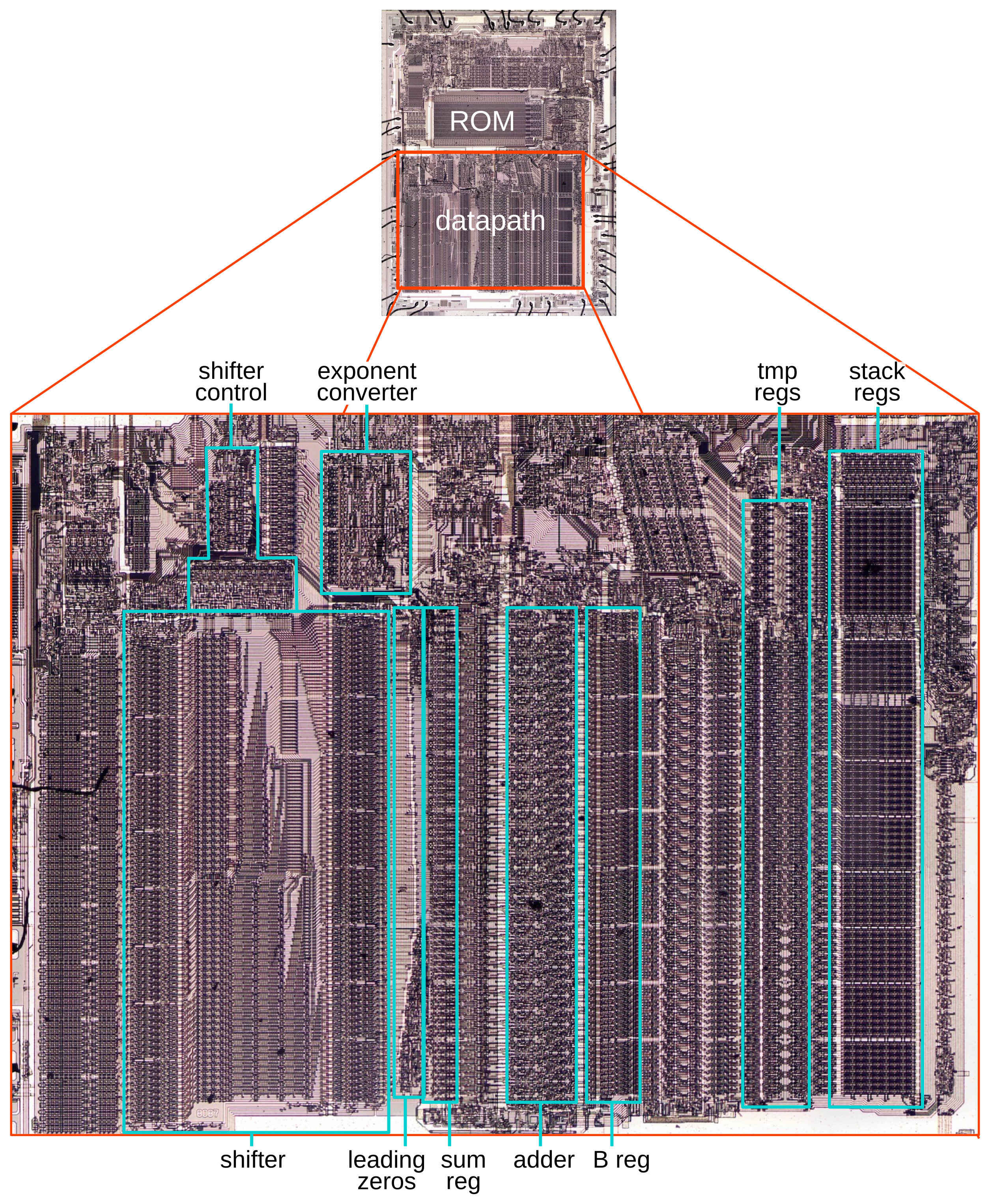
A close-up of the 8087's datapath, showing functional blocks that are used for addition and subtraction. Click this image (or any other) for a larger version.

A close-up of the 8087's datapath, showing functional blocks that are used for addition and subtraction. Click this image (or any other) for a larger version.

Zooming in on the datapath shows the functional blocks that are important for addition and subtraction. The key component is the integer adder, located in the center. It receives one argument from the B register and another argument from a component such as the temporary registers or the stack registers. The adder's output is stored in the sum register. The shifter can shift the bits in a value to the left or the right. The shifter occupies a lot of space on the die because its circuitry allows a value to be rapidly shifted by an arbitrary number of bits. Floating-point operations make heavy use of the shifter to align values; the leading zero circuitry counts the number of zero bits or bytes on the left of a value so they can be shifted away. The exponent converter processes exponents, detecting overflows and underflows. These specialized circuits helped the 8087 achieve its high performance.

Floating-point addition and subtraction

Most computers use integers as their basic representation for numbers. But many applications need to use numbers with a fractional part, such as 1.23. Moreover, integers have a very limited range: a 32-bit integer can express numbers from about -2 billion to 2 billion. To solve these problems,3 computers usually implement floating-point numbers, which provide fractional numbers over an enormous range.

In most cases, a floating-point number is represented by sign × significand × 2exponent. The significand is a binary number of the form 1.bbb…: a leading 1, followed by the binary point (the binary equivalent of the decimal point) and the rest of the bits.4 In a binary number, each bit represents a power of 2. For the fractional part, the part after the binary point, the powers of 2 are negative: 2-1, 2-2, and so forth. So the binary number 1.1 is 1 + 1/2, or 1.5 in decimal. Similarly, binary 1.0011 is 1 + 1/8 + 1/16 or 1.1875. The exponent allows numbers to escape the limited range of the significand. For instance, 1.1 (binary) × 28 is 384. With larger exponents, floating-point numbers can cover a huge range; even a 32-bit short floating-point number covers a range exceeding 10-36 to 1038.

Floating-point addition and subtraction are more complicated than integer operations. Before the numbers can be added (or subtracted), their binary points must be aligned, the same as aligning the decimal points for decimal numbers. After the operation, the exponent of the result must be adjusted, normalizing the significand so it starts with a 1 bit.
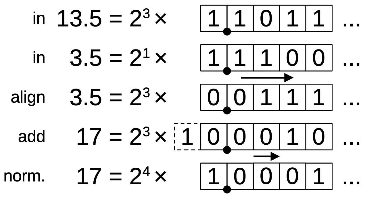
The steps for a simple floating-point addition.

The steps for a simple floating-point addition.

The diagram above illustrates a simple floating-point addition: 13.5+3.5. The first two lines show the two arguments expressed with an exponent and significand. Both arguments are normalized, so the leftmost bit is a 1. Before adding, the second argument must be aligned—making the exponents equal—by shifting it two positions to the right. (The difference between the exponents in this case is two.) The values are then added, using integer addition on the aligned significands. In this case, adding the values causes an overflow, an "extra" bit on the left. The result must be normalized by shifting it one position to the right and incrementing the exponent by 1.

Floating-point subtraction is similar, but has a few more complications. The result can be positive, negative, or zero. The result can be orders of magnitude smaller than the arguments. The figure below shows a basic subtraction, 8-7.5. As with addition, the second argument is shifted right so the exponents match (i.e., the binary points line up). The two significands are subtracted with integer subtraction. The result is normalized by shifting to the left so the top bit is a 1. Unlike the addition case, normalization may require a large shift. In this case, the shift is four bits and the exponent is decremented by 4 to yield the result.
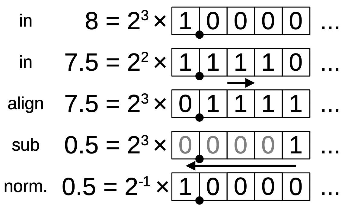
A simple floating-point subtraction.

A simple floating-point subtraction.

One complication with subtraction is that the result can be negative. If that occurs, the significand is made positive, and the sign of the result is flipped. Subtraction can also result in zero. In this case, normalization cannot be performed; instead, a special value +0 or -0 is returned as appropriate.

Relevant hardware details of the 8087

In this section, I'll explain some features of the 8087 that play important roles in the microcode implementation of addition and subtraction.

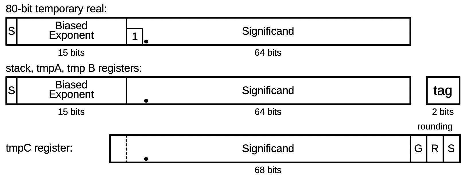
The 8087 supports a variety of data types, but internally, the 8087 stores numbers in an 80-bit format called "temporary real". A temporary real number has a sign bit, a 15-bit exponent, and a 64-bit significand. The 15-bit exponent allows numbers that are absurdly large, over 104932. The 64-bit significand supports extremely accurate numbers. The exponent is stored with a "bias" of 16383 added to it. Thus, the stored exponent is always positive, even if the real exponent is negative. For instance, an exponent of 1 is stored as 0x4000, and an exponent of -16 is stored as 0x3fef.
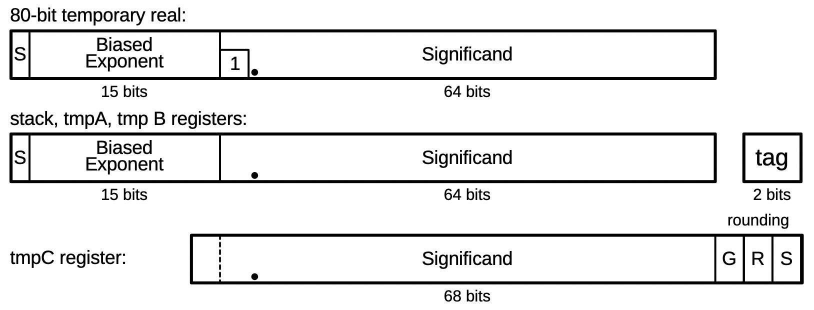
The 80-bit temporary real format and the register formats. The dot indicates the binary point, analogous to the decimal point.

The 80-bit temporary real format and the register formats. The dot indicates the binary point, analogous to the decimal point.

The 8087 has eight internal registers, organized as a stack. The programmer uses these registers when programming the 8087. Each register holds an 80-bit floating-point number. To optimize performance, each value in the register stack also has an associated "tag" value: zero, valid, special, or empty. A value of zero is tagged as zero. A "normal" floating-point value is tagged as valid. If the value is infinity, Not a Number (NaN), or a denormalized value, then it is tagged as special. Finally, an empty tag indicates that a register does not hold a value; this allows detection of stack underflow (reading an empty register) or stack overflow (storing to a non-empty register).

The 8087 also has temporary registers that it uses internally. tmpA and tmpB are 80-bit registers, along with two tag bits. However, tmpC is different: it doesn't have a sign, exponent, or tag. Moreover, the significand is 68 bits; tmpC has an additional bit to prevent overflow and three additional low-order bits for rounding, known as guard, round, and sticky.

In the microcode, each 16-bit micro-instruction performs one low-level operation. Many of the operations move data from one register to another. Other operations provide conditional jumps, subroutine calls, and returns.

The heart of the 8087's processing is the 69-bit integer adder, which I discussed here. (The adder has more than 64 bits because it has three rounding bits and a couple of additional high-order bits for overflow and multiplication.) Integer addition takes two micro-instructions. The first micro-instruction specifies the first argument to add and selects various options such as carry and rounding. (For subtraction, an option complements the second argument.) The second argument to the adder always comes from the B register, which confusingly is unrelated to the tmpB register. The result of the addition operation is placed in a special register called the sum register. A second micro-instruction (which may be many instructions after the first) moves the result from the sum register to a destination.

Floating-point also makes extensive use of the bit shifter, which shifts a 68-bit value by an arbitrary number of positions, left or right; I wrote about it here. Like the adder, a bit shift operation takes two micro-instructions: the first moves a value to the shifter and configures the direction and amount of shift. The second micro-instruction moves the result from the shifter to a destination.

The addition/subtraction microcode

The 8087 implements almost all of its operations in microcode. The basic math operations (addition, subtraction, multiplication, and division) start by executing the same microcode (at decimal address #0001. The microcode moves the two arguments into temporary registers tmpA and tmpB. Normally, these arguments are taken from the stack registers. The arguments can also be taken from memory, but I won't discuss that here.

Next, the microcode does a micro-subroutine call to handle the specific operation type. The 8087's microcode engine has a tiny ROM that holds a table of addresses, targets for microcode jumps or subroutine calls. Target 0 is special, however; it has three different addresses for multiplication, division, or addition/subtraction. (This is implemented by special-case circuitry in the ROM. When you're designing the chip, you can do weird, hacky optimizations like this if you want.)

The addition/subtraction micro-subroutine starts at address #0232; this microcode is shown below. The control flow is complicated, so I've put a flowchart in the footnotes.5 The microcode first handles the zero cases 0+0 or 0-0. Next, it subtracts the exponents of the two arguments. If the first argument has a smaller exponent (i.e., the result is negative), the arguments are swapped so the argument with the larger argument is first. (The 8087 keeps track of the sign of the result in the "sign latch"; if exchanging the arguments would change the sign, the latch is toggled at #0244.)

#0232 jmp #0236 if not tmpA:tag ZERO Check for 0+0
#0233 jmp #0236 if not tmpB:tag ZERO
#0234 return if not unsigned sub 0+0 same signs
#0235 jmp #0263            handle 0+0 different signs
#0236 tmpA sign -> sign latch nonzero: tmpA sign to sign latch
#0237 tmpB:exp -> Breg
#0238 adder: tmpA:exp - Breg cin=1 compare exponents
#0239 jmp #0245 if adder pos
#0240 sumreg:frac -> Breg  swap if tmpB's exponent larger
#0241 adder: zero - Breg cin=1
#0242 xchg tmp
#0243 jmp #0245 if not unsigned sub
#0244 !sign latch -> sign latch toggle sign if swapping matters
#0245 xchg tmp             continue
#0246 shift zero R 0 bytes, 0 bits zero
#0247 call CREATE_DENORM   shift tmpB to match exponents
#0248 xchg tmp
#0249 zero -> tmpB:exp     store exp adjustment in tmpB:exp
#0250 jmp #0269 if not unsigned sub base addition?
#0251 adder: tmpA:frac - Breg cin=1, roundmode tmp A - tmpB
#0252 jmp #0256 if adder pos
#0253 sumreg:frac,rnd -> Breg/rnd negate frac
#0254 adder: zero - Breg cin=1, roundmode
#0255 !sign latch -> sign latch toggle sign
#0256 jmp #0275 if Sum register is zero jump if result zero
#0257 shift R -> tmpB:frac orig tmpB, from CREATE_DENORM
#0258 jmp #0282 if tmpA top bit tmpA not denorm?
#0259 jmp #0282 if tmpB:frac[63] tmpB not denorm?
#0260 jmp #0289            skip normalization if both denorms
#0261 tmpA:exp -> expConv  handle zero
#0262 jmp #0264 if not tmpA top bit
#0263 zero -> tmpA         handle zero cases
#0264 0 -> tmpA sign       +0
#0265 zero -> tmpA:frac
#0266 return if not round chop
#0267 1 -> tmpA sign       return -0
#0268 return
#0269 adder: tmpA:frac + Breg cin=0, roundmode base addition: tmpA + tmpB
#0270 jmp #0289 if not sumreg[64] check for overflow
#0271 shift 1 sumreg:sign,frac,rnd R shift right 1 bit to normalize
#0272 shift R -> sumreg:frac,sign,rnd
#0273 expAdj++             increment exp adjustment
#0274 jmp #0289            wrap up addition
#0275 shift sumreg:frac,rnd L 0 bytes, 3 bits zero? shift to get rounding bits
#0276 shift L -> sumreg:frac
#0277 jmp #0261 if Sum register is zero jump if no rounding bits
#0278 zero -> sumreg:frac  clear result
#0279 jmp #0289 if not tmpA top bit denorm?
#0280 expAdj--             if not denorm, adjust exp down
#0281 1 -> sumreg:frac,rnd set lowest bit in result
#0282 lzcount -> shiftcountH leading zero adjust: handle bytes
#0283 shift sumreg:frac,rnd L count byte sticky
#0284 shift L -> sumreg:frac,rnd
#0285 lzcount -> shiftcountL handle leading zero bits
#0286 shift sumreg:frac,rnd L count bit sticky
#0287 shift L -> sumreg:frac,rnd
#0288 shiftcount -> tmpB:exp remember the bit shift amount
#0289 sign latch -> tmpA sign store sign
#0290 call ADJUST_PRECISION if not FBLD/FBSTP adjust precision if necessary
#0291 sumreg:frac -> tmpA:frac store adjusted frac part
#0292 tmpB:exp -> Breg     get exp
#0293 adder: tmpA:exp - Breg cin=0 adjust by Breg
#0294 expAdj -> Breg
#0295 adder: sumreg:frac + Breg cin=0 adjust by expAdj
#0296 sumreg:frac -> expConv exp in expConv to check for overflow, etc
#0297 sumreg:frac -> tmpA:exp store exp in tmpA
#0298 return               done

At address #0247, the important alignment step takes place, shifting tmpB so the binary point lines up with tmpA. This is done by the microcode subroutine CREATE_DENORM. The number of positions to shift tmpB is passed in the sum register; the difference between the two exponents was calculated in the previous subtraction. (If the difference was negative, it was complemented, so the value passed in is positive.)

Typically, the exponent of the result will be the same as the exponent of the (larger) value, but not always. Changes to the exponent are tracked in two places. First, a special two-bit register that I call the exponent adjustment (expAdj) holds adjustments due to one-bit shifts left or right. The hardware initializes the expAdj register to 1 so there is room for a decrement. Larger exponent changes are tracked in the tmpB register's exponent field; the microcode initializes it to 0 at #0249.

At address #0250, the microcode makes a key decision: is the low-level operation unsigned addition or unsigned subtraction? Depending on the signs involved, the high-level operation (addition or subtraction) may not match the low-level operation. For example, for 2+3, -2-3, -2+(-3), and so forth, the two unsigned numbers are added; the result is 5, either positive or negative. But for -2+3, 2-3, 3-2, and so forth, the two unsigned numbers are subtracted; the result is 1, either positive or negative. I'll use "unsigned addition" to refer to the former cases, where the unsigned magnitudes are added, and "unsigned subtraction" to refer to the latter cases, where the unsigned magnitudes are subtracted. The key point is that an addition instruction may result in unsigned addition or subtraction, and the same with a subtraction instruction.

The 8087 has specialized circuitry to determine whether the low-level unsigned operation is addition or subtraction, allowing this to be tested with a conditional. The tmpA and tmpB values have sign bits of 1 for negative, 0 for positive. If you assign 1 to subtraction and 0 to addition, then tmpAsign⊕​tmpBsign⊕op yields 1 if the unsigned operation is subtraction and 0 if the unsigned operation is addition. The 8087 also has a conditional to test if the signs are the same or different.

Unsigned addition

Since the unsigned addition path is simpler, I'll start with it, at address #0269. The steps are essentially the same as described earlier: aligning the numbers, adding them, and normalizing. First, the smaller number, in tmpB, is shifted right until the exponents match. Then the (unsigned) values are added. If there is a carry from the top bit, the result is shifted right at #0271. Because the result is shifted right one bit, the special two-bit expAdj counter is incremented to track the required exponent adjustment.

At #0289, the result's sign is updated with the value in the sign register. The 8087 supports three sizes of values: 80-bit temporary reals, 64-bit reals, or 32-bit reals. For the smaller sizes, the microcode subroutine ADJUST_PRECISION trims the value to the appropriate size. (This is not as trivial as it sounds, since rounding up the result could require an adjustment to the result's exponent, recorded in the expAdj register.) Finally, the result's exponent is calculated from the initial exponent (in tmpA), subtracting the adjustment value in tmpB's exponent (normally 0), adding the adjustment value in the expAdj register, and subtracting 1 (because expAdj starts at 1). The exponent is stored in the result but also stored in the "exponent converter", a circuit that evaluates the exponent to detect overflow or underflow.

At this point, the addition/subtraction micro-subroutine returns to the common microcode. The common microcode checks if there was an overflow or underflow, indicating the value doesn't fit in a float. In this case, the subroutine NONNORMAL_RESULT is called to handle the value, which can involve triggering an interrupt, returning infinity, or returning zero. (For details, see my previous article.)

The result is pushed on the stack by writing it to the appropriate stack register. If the original instruction specified a stack pop at the end, the top of stack is marked empty, and the stack pointer is updated. Finally, the Run Next Instruction micro-instruction indicates the end of the microcode for the current instruction. The floating-point instruction has finally completed.

Unsigned subtraction

I'll switch now to the unsigned subtraction path, starting at #0251. (Keep in mind that the instruction could be addition, for example, -2 + 3.) The microcode uses the 64-bit adder to perform an unsigned subtraction: tmpA-tmpB; the second argument is negated to perform subtraction. The result can be either positive or negative, depending on which value is larger. The rest of the path is the same as addition: setting the sign, adjusting the precision, and computing the final exponent.

If the subtraction result is zero, #0275 tests the three rounding bits. If a rounding bit is set, then the low bit of the result is set, and the exponent adjustment is decreased by 1 to counteract this. (For a denorm, the result is cleared since there's no "extra" room to promote the rounding bit.) There's a special path #0261 if the result is really zero, because the microcode needs to determine if the result is +0 or -0. Subtracting 0-0 joins into this code path to handle the various possibilities for adding or subtracting +0 and/or -0. Generally, positive and negative zeros work as you'd expect from a zero that "leans" one way. For instance, ⁺0 + ⁺0 is ⁺0 and ⁻0 - ⁺0 = ⁻0. But what if the zeros cancel? E.g. ⁺0 + ⁻0 or ⁻0 - ⁻0? In these cases, rounding down yields ⁻0 while the other rounding modes yield ⁺0.

The leading zero circuit counts the number of leading zeros to determine how much to shift. To keep the circuitry manageable, the leading zero shift is done in two steps. First, the result is shifted left by the number of leading zero bytes. Next, the leading zero circuitry counts the number of remaining leading zero bits, which will be 0 to 7 at this point. The result is shifted left by that many bits. The total shift amount is stored in tmpB's exponent.

The unsigned subtraction path merges at #0289 with the unsigned addition path described earlier, adjusting the precision, computing the exponent, and storing the result. The micro-subroutine then returns to the common code that also handles multiplication and division.

Special-case handling in the common microcode

The 8087 handles many special cases for infinities, zeros, Not-a-Number, denormals, and other special values. The designers of the 8087 carefully thought about these special cases and attempted to handle them in mathematically reasonable ways.6 The table below is just part of the special cases that the 8087 handles.
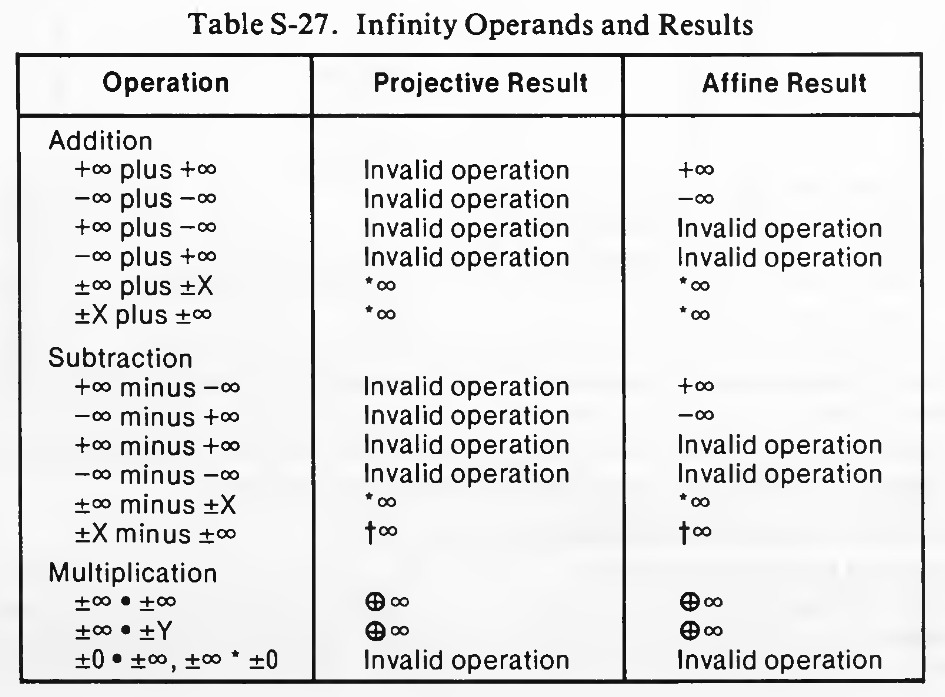
Part of the special-case handling of infinities as described in the User's Manual.

Part of the special-case handling of infinities as described in the User's Manual.

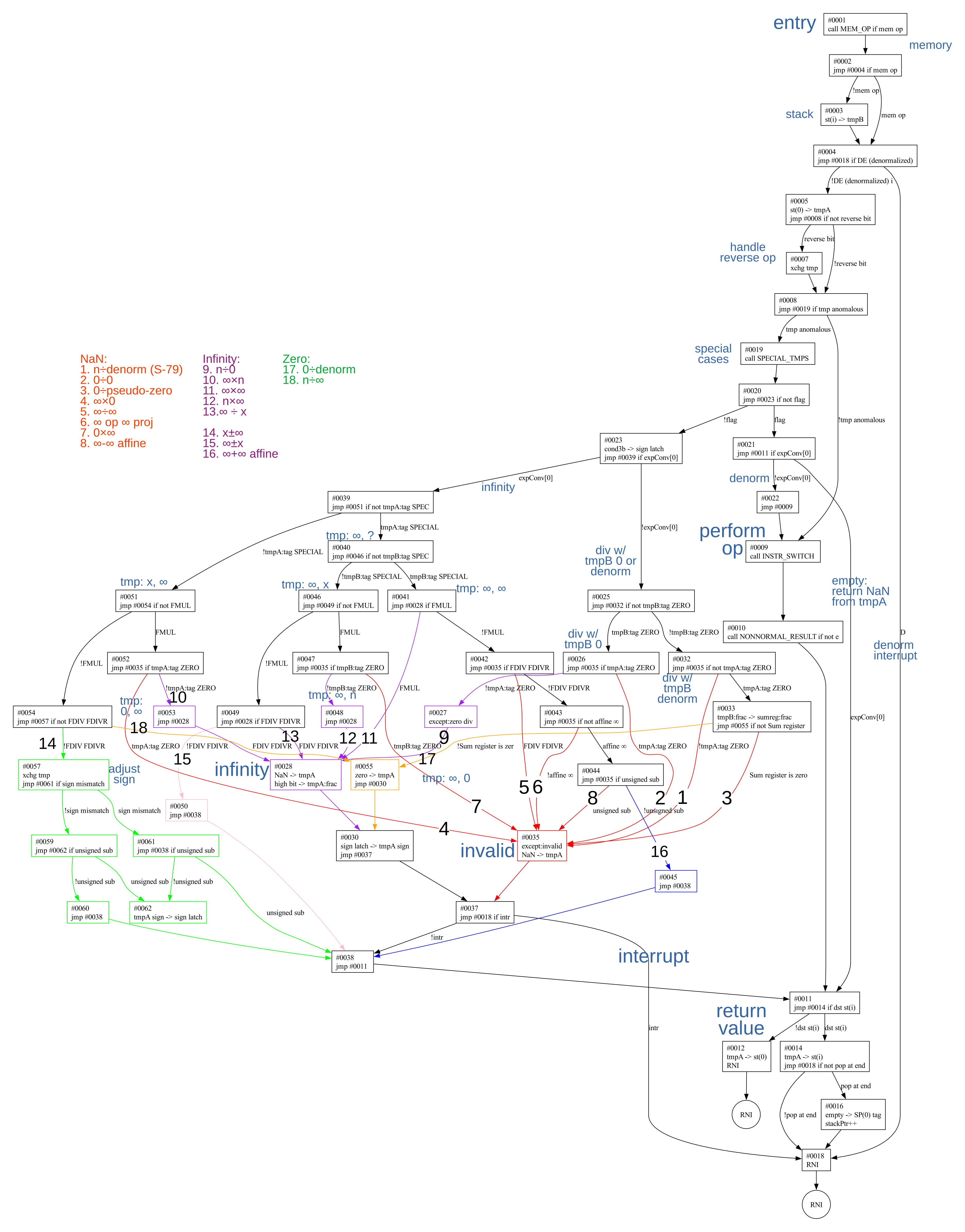
While these special cases make the 8087 more accurate mathematically, they make the microcode much more complicated. The microcode below is common to addition, subtraction, multiplication, and division. It loads arguments and stores the result as described above, but for the most part, it handles special cases. This microcode is "spaghetti code", with 18 conditional branches in a row to handle numerous special cases. I'll describe it at a high level here; the flowchart in the footnotes7 provides details.

#0001 call MEM_OP if mem op maybe get args from memory
#0002 jmp #0004 if mem op
#0003 st(i) -> tmpB        get from stack
#0004 jmp #0018 if DE (denormalized) interrupt quit if denormalized interrupt
#0005 st(0) -> tmpA        top of stack to tmpA
#0006 jmp #0008 if not reverse bit no jump if FSUBR, FMUL, FDIVR?
#0007 xchg tmp             reverse arguments
#0008 jmp #0019 if tmp anomalous handle anomalous values
#0009 call INSTR_SWITCH    switch on instruction type: J1(mul), J2(add/sub), J3(div)
#0010 call NONNORMAL_RESULT if not exp normal Back, finish up instruction
#0011 jmp #0014 if dst st(i) test d destination bit
#0012 tmpA -> st(0)        destination st(0)
#0013 RNI
#0014 tmpA -> st(i)        exit: destination st(i)
#0015 jmp #0018 if not pop at end RNI if not pop
#0016 empty -> SP(0) tag   mark top of stack empty
#0017 stackPtr++           pop
#0018 RNI
#0019 call SPECIAL_TMPS    handle special values
#0020 jmp #0023 if not flag
#0021 jmp #0011 if expConv[0] jump to finish
#0022 jmp #0009            switch on instruction type
#0023 cond3b -> sign latch more conditions
#0024 jmp #0039 if expConv[0]
#0025 jmp #0032 if not tmpB:tag ZERO
#0026 jmp #0035 if tmpA:tag ZERO
#0027 except:zero div
#0028 NaN -> tmpA          NaN, finish
#0029 high bit -> tmpA:frac
#0030 sign latch -> tmpA sign
#0031 jmp #0037            finish up
#0032 jmp #0035 if not tmpA:tag ZERO divide by denorm/0
#0033 tmpB:frac -> sumreg:frac divide by 0
#0034 jmp #0055 if not Sum register is zero
#0035 except:invalid
#0036 NaN -> tmpA
#0037 jmp #0018 if intr    jump to RNI
#0038 jmp #0011            finish
#0039 jmp #0051 if not tmpA:tag SPECIAL more conditions
#0040 jmp #0046 if not tmpB:tag SPECIAL
#0041 jmp #0028 if FMUL
#0042 jmp #0035 if FDIV FDIVR
#0043 jmp #0035 if not affine ∞ ∞×∞: test if affine
#0044 jmp #0035 if unsigned sub test if ∞ add or subtract
#0045 jmp #0038
#0046 jmp #0049 if not FMUL
#0047 jmp #0035 if tmpB:tag ZERO
#0048 jmp #0028
#0049 jmp #0028 if FDIV FDIVR
#0050 jmp #0038
#0051 jmp #0054 if not FMUL
#0052 jmp #0035 if tmpA:tag ZERO divide by 0?
#0053 jmp #0028
#0054 jmp #0057 if not FDIV FDIVR
#0055 zero -> tmpA         0÷denorm or n÷∞
#0056 jmp #0030            do something and finish up
#0057 xchg tmp
#0058 jmp #0061 if sign mismatch
#0059 jmp #0062 if unsigned sub test if adding or subtracting
#0060 jmp #0038            finish
#0061 jmp #0038 if unsigned sub finish
#0062 tmpA sign -> sign latch complement sign
#0063 !sign latch -> tmpA sign
#0064 jmp #0038            finish

Looking at #0008, the 8087 micro-architecture includes a conditional test that will check if either temporary register is empty or is tagged with a special value. If so, a subroutine that I call SPECAL_TMPS is called.8 It examines the two temporary registers and sets two flags to indicate what special handling needs to be done.

If both flags are set, one of the arguments was tagged empty, typically indicating a stack underflow. In this case, the microcode returns Not-a-Number (NaN). If the second flag is clear, then one of the arguments was a denormal number, a special value very close to zero. The arithmetic operation continues in that case.

The remaining code paths get complicated, for example, branching on the signs of the arguments, the specific arithmetic operation, or if an argument is zero or infinity. Eight code paths return Not-a-Number: n÷denorm, 0÷0, 0÷pseudo-zero, ∞×0, ∞÷∞, 0×∞, ∞ op ∞ proj, and ∞-∞ affine. Many of these are straightforward—0×∞ has no meaningful value, for instance—but the last two need a bit more explanation.

The 8087 has two different modes for infinity, selected by a bit in the control register. With "affine closure", infinity is signed, so +∞ and -∞ are two different values. The recommended mode is "projective closure", where infinity is unsigned. In affine mode, ∞+∞ is perfectly valid, yielding positive infinity. However, ∞-∞ is meaningless; an answer of 0 would be arbitrary, so NaN is returned. In projective mode, none of the operations on infinity make sense because infinity is both infinitely positive and infinitely negative.

The microcode has eight different paths to return infinity: n÷0, ∞×n, ∞×∞, n×∞, ∞÷x, x±∞, ∞±x, and ∞+∞ affine. (The first case assumes that the divide-by-zero exception has been masked.) For the first five cases, the microcode generates the sign for infinity by combining the signs of the arguments. However, the last three cases take the sign from the infinity argument and ignore the other sign. In other words, multiplication and division can flip the sign of an infinity, but addition and subtraction can't.

Two paths deal with special-case 0 results: 0÷denorm and n÷∞. The microcode generates 0 with the correct sign, based on the signs of the arguments.

The leading zeros circuitry

With subtraction, digits can cancel out, leaving leading zeros that need to be removed by shifting the value. The 8087's shifter can shift a 64-bit value by an arbitrary number of bits. The job of the leading-zero circuitry is to count the leading zeros to determine how much to shift. That is, it counts how many zeros are to the left of the first 1 bit and turns this into a binary value. This is basically the same as a priority encoder that encodes the position of the first 1 bit.

Leading-zero circuits are somewhat complicated because each binary output bit depends on all the input bits; a 64-bit detector has 64 bits coming in. One approach is to take the truth table and optimize it, ending up with a pile of logic. Another approach is to use a hierarchical approach, a tree with log(N) stages. The 8087 takes a simpler path: one pass to eliminate leading zeros a byte at a time, and a second pass to eliminate the remaining 0 to 7 leading zero bits. Each pass requires a separate 8-input leading zero detector circuit. This approach is slower, but the circuitry is much simpler: two 8-bit leading zero detectors instead of a 64-bit leading zero detector.

The schematic below shows the circuit that converts 0 to 7 leading zeros into a 3-digit binary value. To simplify the schematic, I've replaced the first layer of logic with a bitmask that represents the 8-bit input. For instance, x01xxxxx indicates that the signal is high if the second bit is 0, the third bit is 1, and the remaining bits are arbitrary. I've added text descriptions; due to optimizations, the descriptions have some exceptions. For instance, x01xxxxx matches anything with two leading zeros. It also matches some patterns with no leading zeros, but those don't change the result. The important thing is that it matches everything with 2 leading zeros and nothing with 1 or 3 leading zeros.
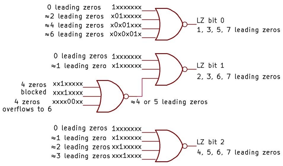
The circuitry to detect 0 to 7 leading zero bits. The same approach is used to detect leading zero bytes.

The circuitry to detect 0 to 7 leading zero bits. The same approach is used to detect leading zero bytes.

The output from the circuit is a 3-bit binary value representing the number of leading zeros. The top NOR gate generates the low bit, set for 1, 3, 5, or 7 leading zeros. The high bit is generated by the bottom NOR gate: set for 4, 5, 6, or 7. The middle bit is trickier, with an additional layer of logic to determine if there are 4 or 5 leading zeros (or maybe 0 or 1). The two 1 cases block four zeros, while the 00 pair means that four leading zeros would turn into at least 6. (This is a hand-waving explanation, but one can enumerate the 256 cases and verify that they all produce the correct answer.)

To count the number of bytes with leading zeros, similar logic is used. However, each group of 8 bits goes through an OR gate to detect if any bits are set in the byte. Thus, the logic determines how many bytes of leading zeros are present.

On the die, the leading zero logic is immediately to the left of the sum register, examining each bit of the sum register.

Conclusions

Most people don't give much thought to computer operations such as addition or subtraction. But there are interesting algorithms and special cases behind the scenes, and these features are embodied in clever silicon circuits. The intricate rules to handle positive and negative zeros, positive and negative infinities, and Not-a-Number are part of modern computers, since the 8087 led to the IEEE-754 floating-point standard used today. The 8087 went a bit overboard with special cases, however. Some 8087 features, such as projective infinity, unnormals, and pseudo-zero were dropped from the standard becauses they weren't worth the effort.

I plan to continue reverse-engineering the 8087 microcode; for updates, follow me on Bluesky (@righto.com), Mastodon (@[email protected]), or RSS. I've been working on this with the members of the "Opcode Collective", especially Smartest Blob and Gloriouscow, who converted the ROM images to microcode data and extensively analyzed the contents. See the 8087 repository on GitHub for more. AI statement: Despite the presence of the em dash, no AI was used in the writing of this article (details). The Opcode Collective used an ML algorithm to classify each ROM cell to extract the microcode.

Notes and references

  1. Intel's documentation provides a performance comparison of the 8087 versus floating-point operations emulated on the 8086. The speedup varies depending on the instruction, but is typically almost a factor of 100. This speedup made the 8087 chip highly desirable for numerical applications such as CAD and spreadsheets. ↩

  2. Internally, the 8087 uses 80 bits to hold floating-point values: one bit for the sign, 15 bits for the exponent, and 64 bits for the significand. However, the 8087 uses three extra low-order bits for rounding, called Guard, Round, and Sticky. These bits ensure that a value is always rounded in the right direction. Some parts of the datapath have additional bits for sign or overflow: the shifter is 68 bits wide, and the adder is 69 bits wide. For the most part, I'll ignore these extra bits and refer to the datapath as 64 bits wide. ↩

  3. While floating-point numbers solve some problems, they introduce problems of their own. For instance, 0.01 can't be expressed exactly in floating point (it has an infinite repeating fraction in binary, just like 1/3 can't be expressed exactly as a decimal number). This can cause havoc if you're using floating-point numbers to represent money and you're dealing with cents. For more on problems with floating-point, see this Julia Evans comic or What Every Computer Scientist Should Know About Floating-Point Arithmetic. ↩

  4. One difference between the 8087's temporary real format and the external formats is that in the temporary real, the leading 1 digit is explicitly stored in the number. In the external formats, the leading 1 is implicit and not stored in the number, providing one additional bit of accuracy, but making arithmetic more complicated. ↩

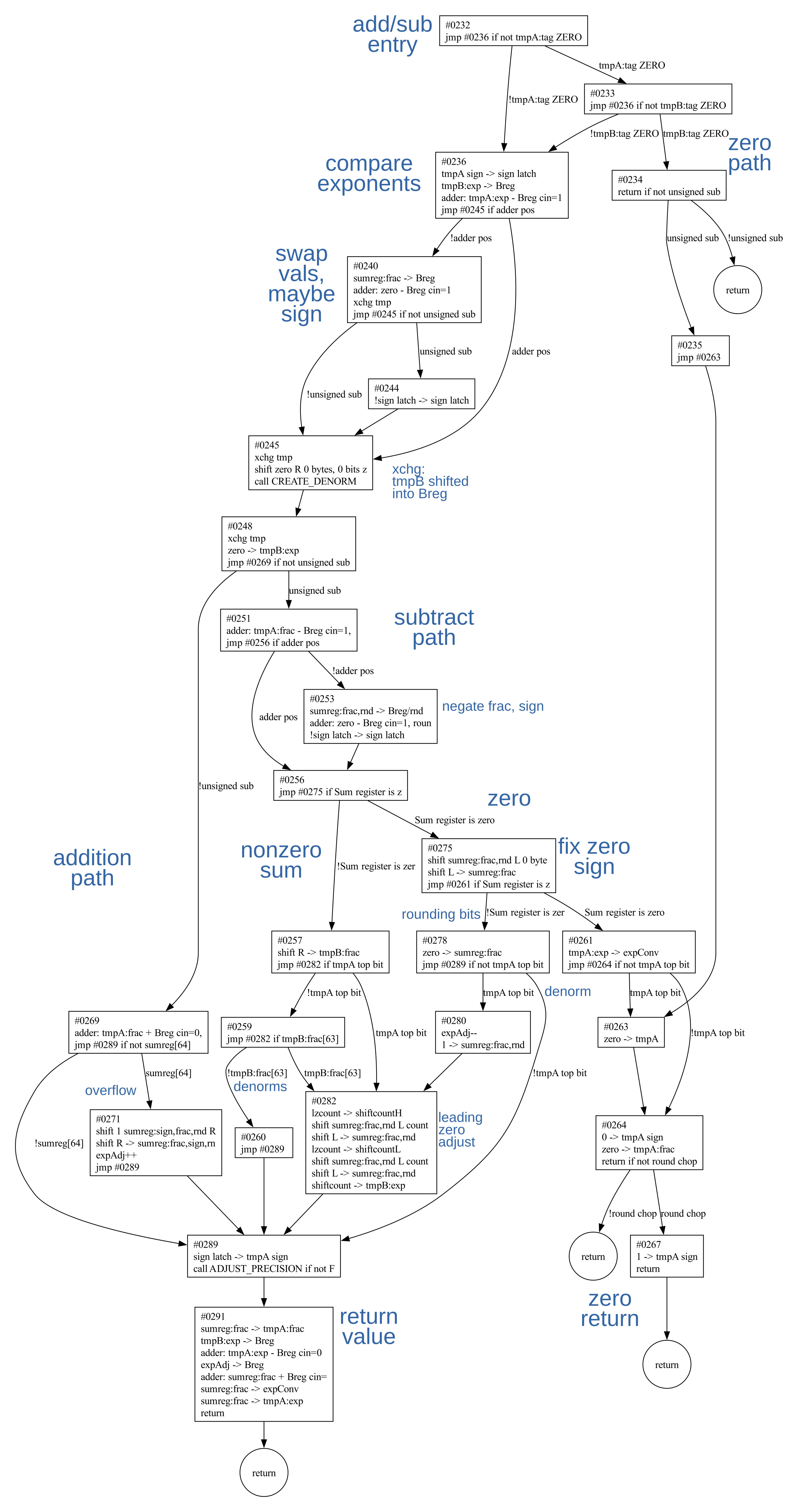
  5. The flowchart below shows the control flow for the addition/subtraction microcode. (Click it for a larger image.)
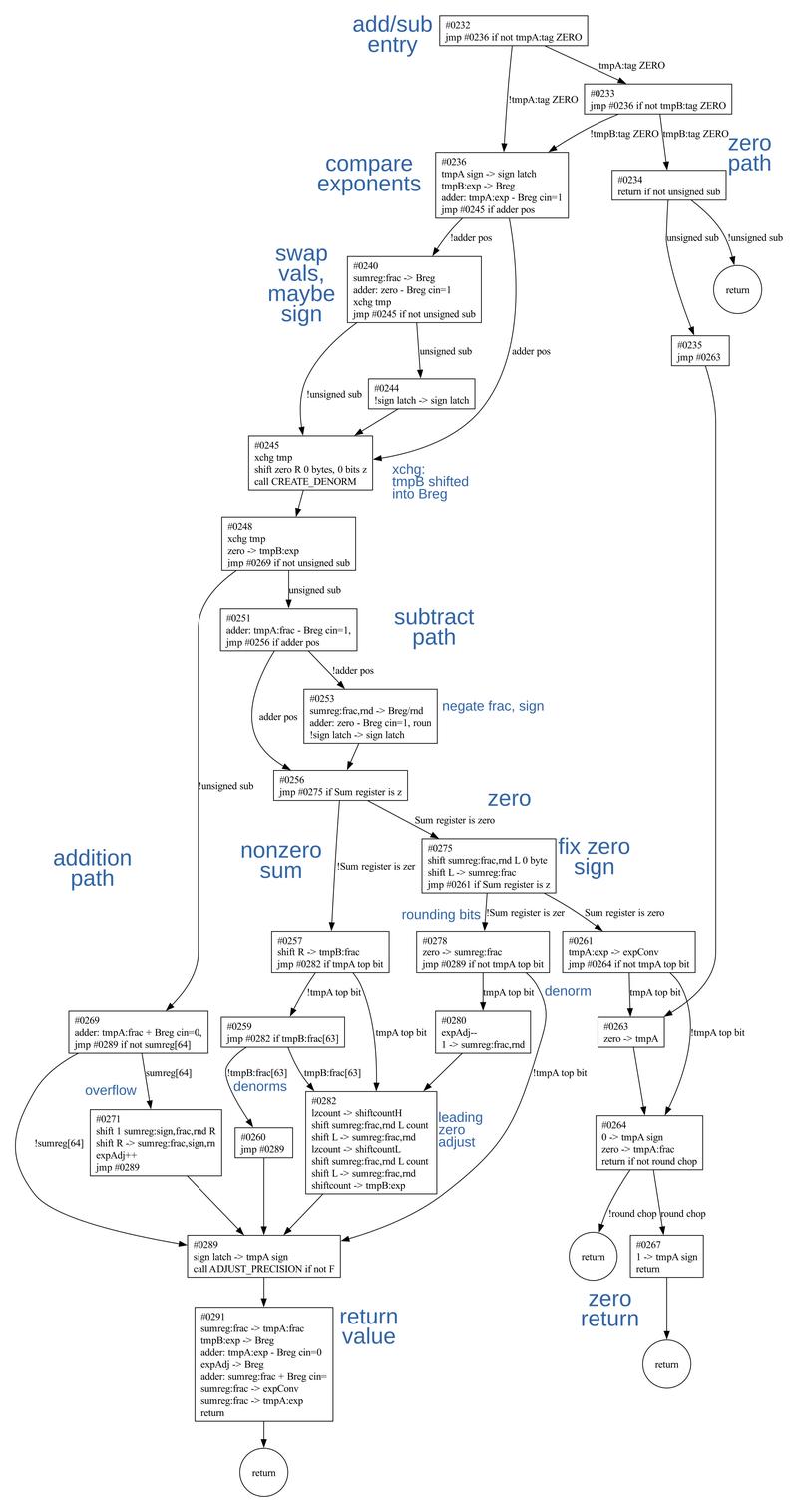
    Flowchart of the add/sub microcode.

    Flowchart of the add/sub microcode.

     ↩

  6. William Kahan is the floating-point expert behind the 8087. He wrote about the motivations for various design decisions here, if you want the details of, for example, why NaN != NaN. (One interesting comment discusses the value of 00, commonly debated online. Kahan states, "A consensus is growing that x**0 = 1 for every x , including 0 , ∞ and NaN.") ↩

  7. The flowchart below shows the microcode that is shared for basic arithmetic instructions. This flowchart calls the above flowchart as a subroutine. The numerous special case paths are numbered.
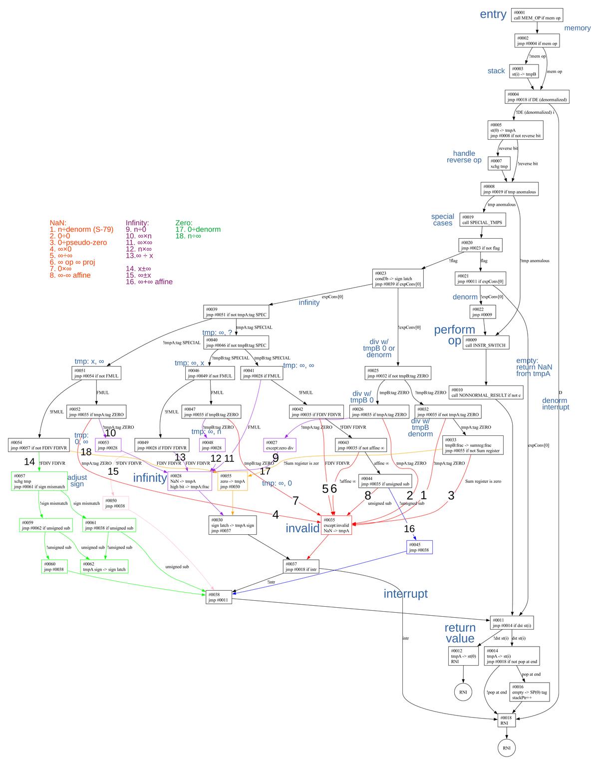
    Flowchart of the common microcode for basic arithmetic operations. (Click for a larger image.)

    Flowchart of the common microcode for basic arithmetic operations. (Click for a larger image.)

     ↩

  8. The actions of SPECIAL_TMPS are summarized below. It returns status through the flag flip-flop and the exponent converter register (expConv). Its actions are:

    InputResultflagexpConv
    emptyNaN, exception11
    NaN(larger) NaN, exception11
    infinityinfinity01
    denormunnorm10
    divide-by-zero(ish)no change00

    The line I call "divide-by-zero(ish)" indicates that a division instruction is attempting to divide by zero or an unnormal number (which is close to zero). I'll give a bit of background on how the 8087 represents 0 and values near 0. A normal floating-point value has a mantissa with the first bit set. Unfortunately, normal numbers have a large gap between the smallest normal number and zero. Denormals break this "rule", allowing the top bits to be zero, so there are many more numbers near 0. (For a base-10 analogy, suppose you count down 1.003, 1.002, 1.001, 1.000. If the top digit must remain set, the next possible number is 0, a huge jump from 1.000. Denormals let you keep going in small steps: 0.999, 0.998, ...., 0.001, 0.)

    For a denormal, the exponent has the smallest possible value. Unnormals are similar to denormals, except the exponent has a larger value. The purpose of unnormals is that if a denormalized exception is masked, the denormal number is converted to an unnormal and execution continues.

    For true zero values, the 8087 uses a signed zero, so you can have either +0 or -0. A true zero is stored with the smallest possible exponent. But the 8087 also supports a "pseudo-zero", a zero value that has a larger exponent. The pseudo-zero can arise from multiplying two very small unnormal values. (With the 80387 floating-point chip, Intel got rid of unnormals and pseudo-zeros.)

    I discussed the microcode for the SPECIAL_TMPS subroutine in detail earlier, so I won't discuss it more here. ↩
Inside a 1980s filter chip that uses switched capacitors

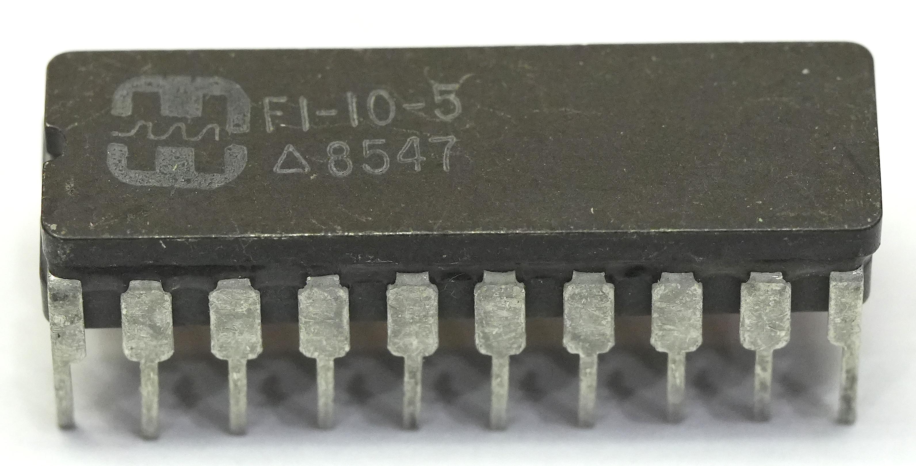
Sometimes it's easier to identify an IC with a microscope. While sorting a box of old ICs, CuriousMarc came across some Harris ICs labeled "F1-10-5", a mysterious part number that didn't show up in any databooks. Since unidentifiable ICs are useless, he gave me one to analyze. Conveniently, it was in a ceramic package, so I could open it up with a quick tap from a chisel. Under the microscope, the chip's most striking feature was a grid of square capacitors. With all those capacitors, I guessed that it was a switched-capacitor filter. The die provided another clue: the part number HF-10. With this information, we quickly found that the chip was Harris's version of the standard MF10 switched-capacitor filter chip.1

The Harris integrated circuit, labeled F1-10-5 (or maybe FI-10-5), with a 1985 date code. Photo courtesy of CuriousMarc.

The Harris integrated circuit, labeled F1-10-5 (or maybe FI-10-5), with a 1985 date code. Photo courtesy of CuriousMarc.

Switched-capacitor filters were a popular way to implement analog filters in the 1980s. Rapidly switching capacitors in and out of a circuit enabled the construction of single-chip filters that were easy to use and performed well. The MF10, introduced by National Semiconductor in 1981, provides two flexible filters on a chip; each filter acts as a low-pass filter, band-pass filter, or a high-pass filter. The filter's characteristics are simple to control with a few external resistors.

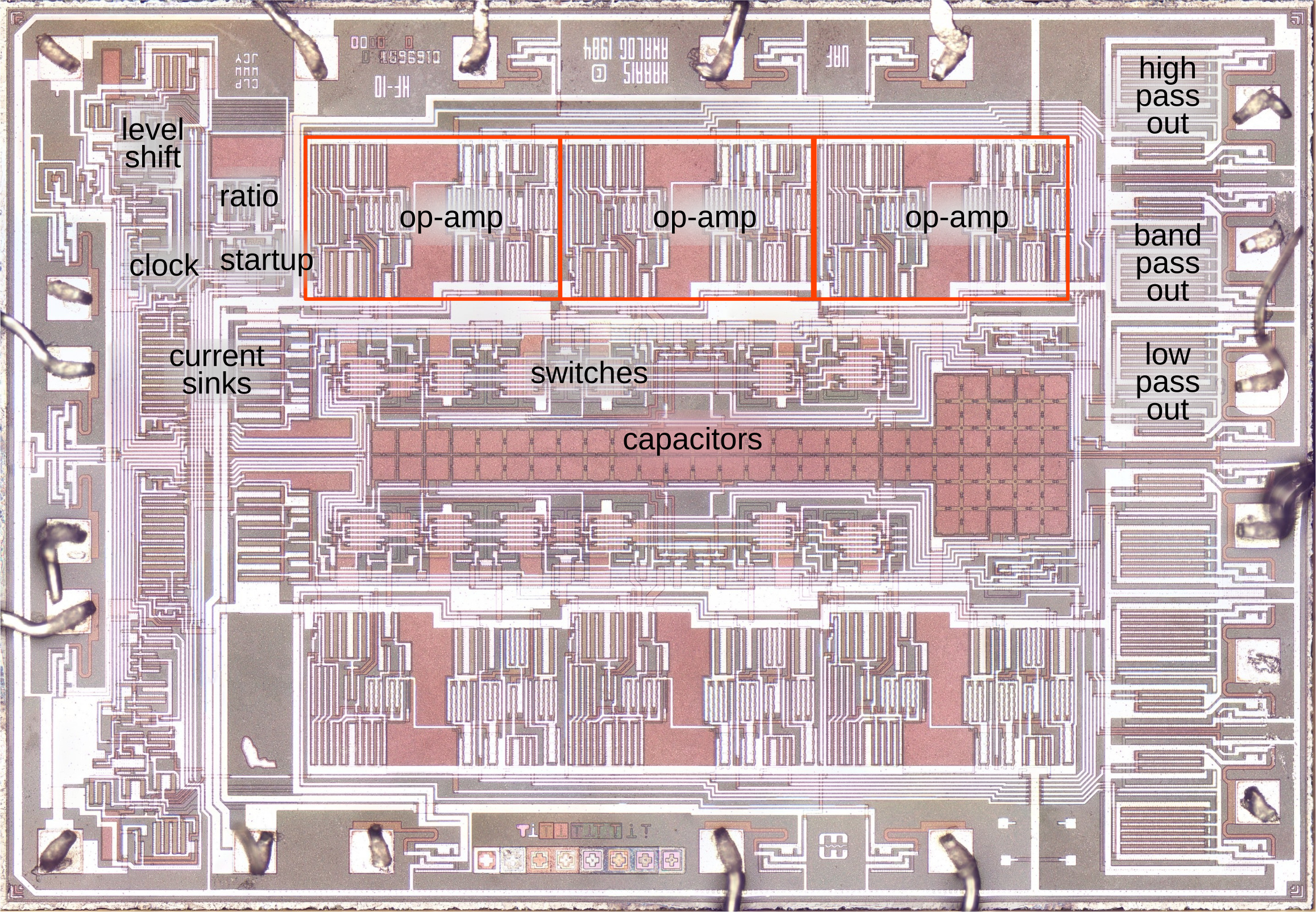
The Harris HF-10 die under the microscope with the main functional blocks labeled. (Click for a larger image.)

The Harris HF-10 die under the microscope with the main functional blocks labeled. (Click for a larger image.)

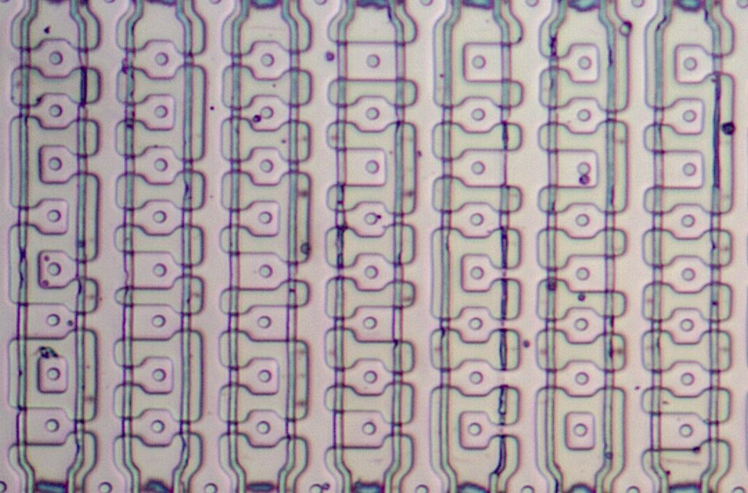
Since I had the chip under the microscope, I took the opportunity to analyze it more closely. The white lines are the metal wiring that connects the chip's circuitry. Under the metal layer are two layers of polysilicon (reddish) and the underlying silicon (gray). The top and bottom halves of the chip are mostly mirror images, corresponding to the chip's two filters. The distinctive reddish squares in the middle of the chip are 72 tiny capacitors, constructed from polysilicon. Above the capacitors, CMOS switches turn on and off at the clock frequency, switching capacitors in and out of the circuit. Each filter uses three operational amplifiers (op amps), outlined in red. At the right are the three outputs from the three op amps: high pass, band pass, and low pass. The control circuitry is on the left: clock level shifting, clock shaping, frequency ratio handling, startup circuitry, and current sinks to provide fixed currents to other parts of the chip. Around the edges of the silicon die, 20 hair-thin bond wires connect the die to its 20 external pins.

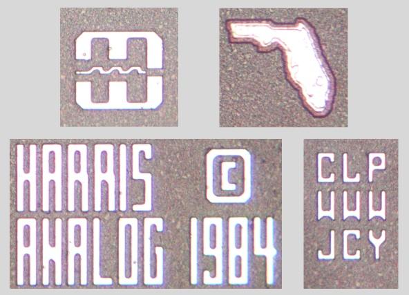
The die has some interesting chip art: a Harris logo and an outline of Florida; Harris was headquartered in Melbourne, Florida. The initials on the die are presumably the engineers who designed the chip.

Some interesting images from the die.

Some interesting images from the die.

Switched capacitor circuits

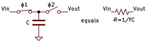
The filter is based on switched-capacitor circuits. A switched capacitor can replace a resistor in certain circuits, as shown below. The switches are controlled by a clock signal; the switches alternately close in clock phase 1 and phase 2 (ϕ1 and ϕ2). In phase 1, the capacitor is charged to the input voltage. In phase 2, the capacitor passes charge to the output. By rapidly toggling the switches, charge is (almost) steadily passed to the output. The larger the capacitance, the more charge that is passed through. Likewise, a higher frequency passes more charge. It can be shown that the circuit matches a resistor with resistance of 1/(fC): a higher capacitance and frequency correspond to lower resistance.

A switched capacitor can replace a resistor.

A switched capacitor can replace a resistor.

Why would you replace a simple resistor with this complicated switching circuit? In an integrated circuit, resistors are inaccurate and inconveniently large, especially high-value resistors. Replacing a large resistor with a small capacitor saves space on the die. Moreover, it is easy to generate an extremely accurate clock frequency with an inexpensive quartz crystal, making the filter's frequency highly accurate. Finally, the equivalent resistance can be changed simply by changing the clock frequency, making it easy to tune or sweep the filter.

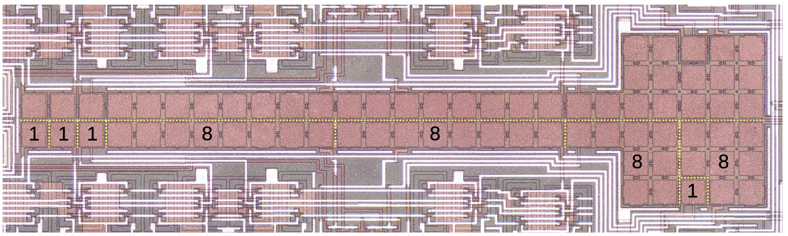
On-chip capacitors are fairly inaccurate, with the capacitance typically varying by 20% from chip to chip due to variations in manufacturing conditions. However, this isn't a problem in the MF10 because the circuitry was designed to depend on the ratio between capacitances, which is stable. Specifically, the MF10 uses 72 identical square capacitors, which will have almost identical capacitances. Careful examination shows that some of the capacitors are separate, while others are connected in groups of 8 to form larger capacitors.2 This yields a highly accurate ratio of 8:1 between the grouped capacitors and the individual capacitors, even though the absolute capacitance will vary from chip to chip. Each capacitor is constructed from two layers of polysilicon,3 forming the plates of the capacitor, separated by a thin layer of insulating oxide that acts as the dielectric. I estimate that each capacitor square is 5 picofarads.

The grid of capacitors in the MF10. I've added yellow lines to show how the capacitors are grouped. The switches are above and below the capacitors.

The grid of capacitors in the MF10. I've added yellow lines to show how the capacitors are grouped. The switches are above and below the capacitors.

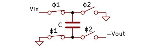
This chip uses one more trick with switched capacitors: it inverts the voltage while acting as a resistor. In the switched-capacitor circuit below, there are four switches. The capacitor charges to the input voltage during phase 1, the same as before. But during phase 2, note that the top plate of the capacitor is grounded, while the output comes from the bottom plate. If the capacitor was charged to, say, 1 volt, the top plate is 1 volt above the bottom plate. So if the top plate is grounded, then the bottom plate must be at -1 V. (This is the same idea as a charge pump.) This circuit turns out to yield a more accurate filter because some parasitic capacitances cancel out.

By using four switches, the switched capacitor can invert the voltage.

By using four switches, the switched capacitor can invert the voltage.

The op-amp integrator

The heart of most analog circuits is the operational amplifier, or op-amp. An op-amp takes two inputs and amplifies the difference by many orders of magnitude. Normally, an op-amp is configured with negative feedback, which forces the two inputs to be essentially the same. Op-amps are useful not only for amplification, but for filtering, buffering, summing, and other tasks.

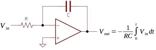
A basic op-amp integrator.

A basic op-amp integrator.

The filter chip uses op-amps as integrators, to integrate an input voltage over time. The circuit above shows a simple op-amp integrator. The input voltage produces a current that flows through the resistor and charges the capacitor, so the capacitor holds the integral of the input voltage over time. You might expect that the left side of the capacitor would become positive as it charges. However, the op-amp's feedback forces both inputs to ground, so instead the right side of the capacitor becomes negative. Thus, the output is the negative integral.4

The MF10 chip uses the circuit above, except the resistor is replaced with a switched capacitor. The capacitor across the op-amp is not switched, but consists of either 8 or 16 capacitors from the capacitor grid.

The CMOS switches

The CMOS switch is the technology that makes the switched-capacitor filter possible. A CMOS switch has a fairly low resistance (maybe tens of ohms) when closed and an enormously high resistance (hundreds of megohms) when open. This high resistance ensures that the charge doesn't leak out of the capacitors.

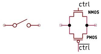
A CMOS switch is constructed by combining an NMOS transistor and a PMOS transistor. The NMOS transistor and PMOS transistor are opposites. An NMOS transistor is good at pulling the output low, while a PMOS transistor is good at pulling the output high, so in combination they provide an effective switch. An NMOS transistor is turned on by a high voltage on the gate, while a PMOS transistor is turned on by a low voltage on the gate. Thus, a CMOS switch requires two control signals of opposite polarity, which is a minor inconvenience.

A CMOS switch.

A CMOS switch.

The diagram above shows how a switch is implemented with an NMOS transistor and a PMOS transistor in parallel. When the control line is high, and the inverted control line is low, both transistors turn on, providing a path through the switch circuit. When the control line is low (and the inverted line high), the transistors turn off, opening the switch.

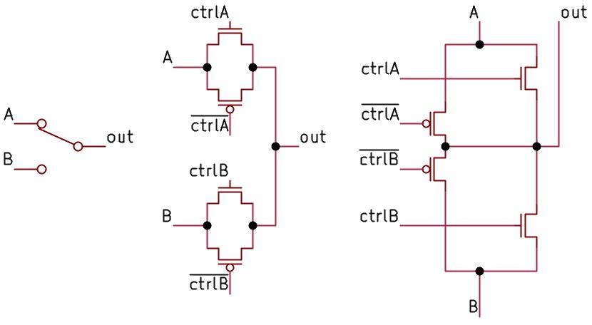
The chip uses CMOS switches in pairs, with one switch on and the other off. This forms the equivalent of a toggle switch that connects either A or B to the output. This circuit is simply two CMOS switches, with separate control lines for each switch, as shown below. In the MF10, the switch toggles at the clock frequency. During one clock phase, the switch is connected to A, while the switch is connected to B during the other clock phase. The schematic on the right, below, is the same circuit, but reorganized to match the layout on the die.

A double-throw CMOS switch.

A double-throw CMOS switch.

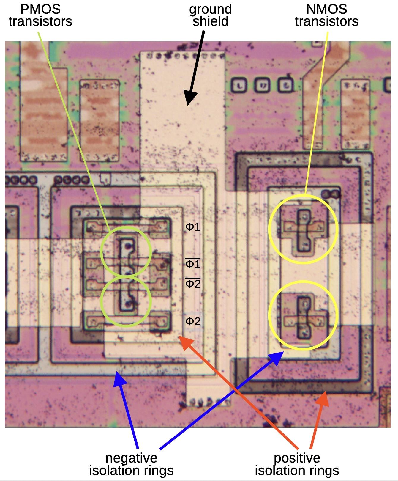
The photo below shows a CMOS switch on the die, constructed from two PMOS transistors and two NMOS transistors. The four control lines run horizontally in polysilicon, forming a transistor gate where they cross doped silicon. The upper PMOS and NMOS transistors are driven by the clock phase 1 (Φ1) signals, while the lower transistors are driven by the phase 2 signals.

CMOS switches on the die. The metal layer was removed to show the transistors.

CMOS switches on the die. The metal layer was removed to show the transistors.

One problem with switched-capacitor filters is that the clock can generate switching noise that appears in the chip's outputs. The MF10 uses several techniques to reduce clock noise. Each set of transistors is surrounded by two isolation rings: one positive and one negative. These block noise from traveling through the silicon substrate. Note that the rings have opposite polarity for the NMOS transistors and the PMOS transistors. The light tan region in the photo above is a second layer of polysilicon. This polysilicon is connected to ground, providing a shield layer over the switching circuits.

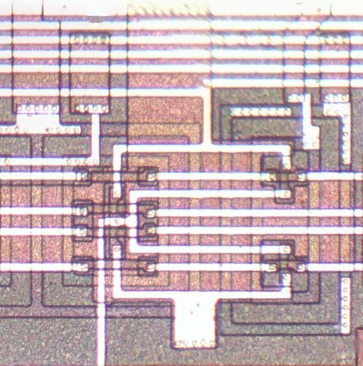
For the photo above, I removed the metal layer with acid5 to make the transistors more visible. The photo below shows the original die, with the metal layer connecting the transistors. The small black circles are connections between the metal layer and silicon or polysilicon.

The same CMOS switches, showing the metal layer.

The same CMOS switches, showing the metal layer.

Putting it together: the state variable filter

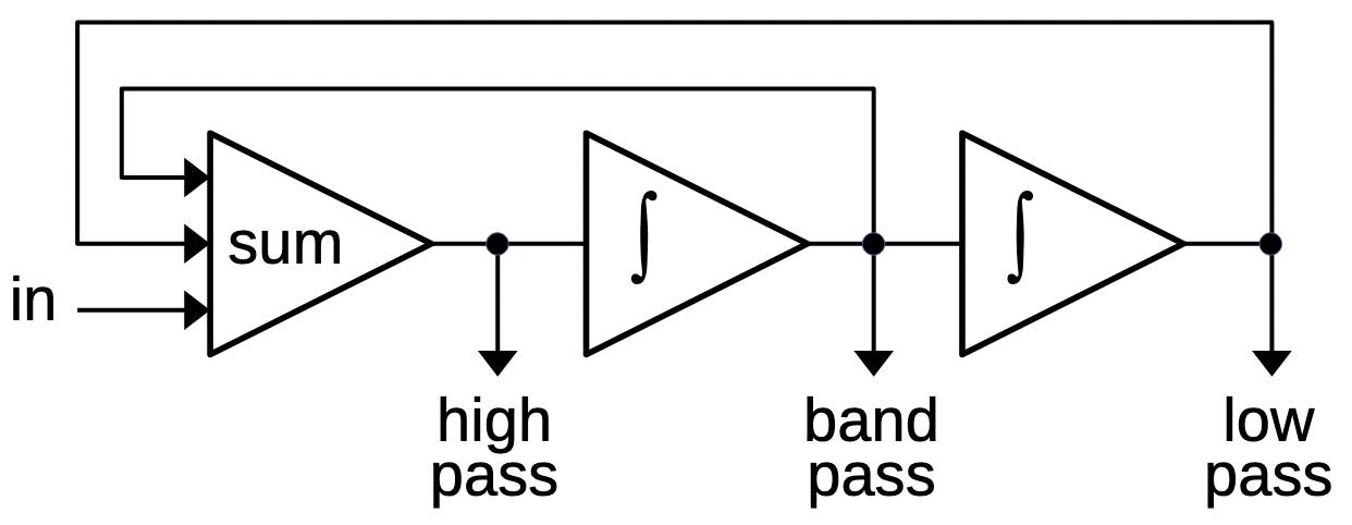
There are many ways of creating a filter. The MF10 chip uses a technique called the state variable filter, invented in 1967. This circuit acts as three filters, with high-pass, band-pass, and low-pass outputs. Moreover, the circuit is flexible since the frequency, the gain, and the filter quality (Q) can be varied independently. It uses three op-amps: one to sum signals and two for integration. By changing how the values are summed, the characteristics of the filters can be changed. The diagram below shows a simplified representation of a state variable filter. The mathematics behind a state variable filter is complicated, so I won't get into it. In short, the signal, the integral, and the double integral form the three state variables that define the state of the system.

Simplified diagram of a state variable filter, with two integrators. Inspired by North Coast Synthesis.

Simplified diagram of a state variable filter, with two integrators. Inspired by North Coast Synthesis.

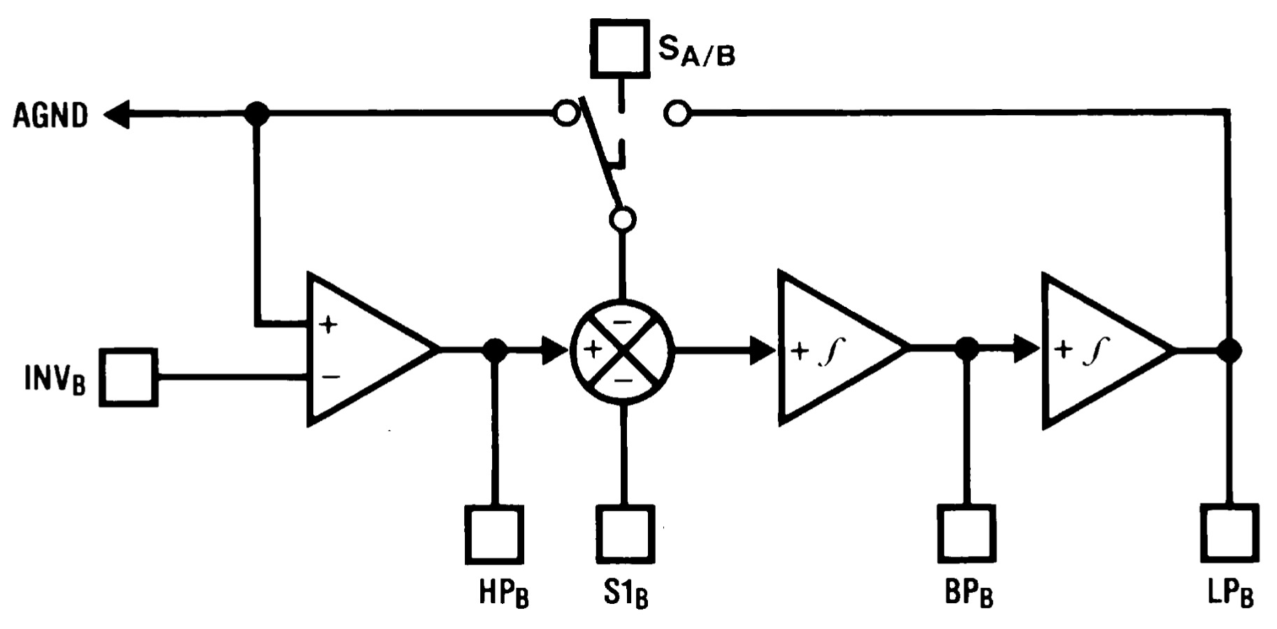
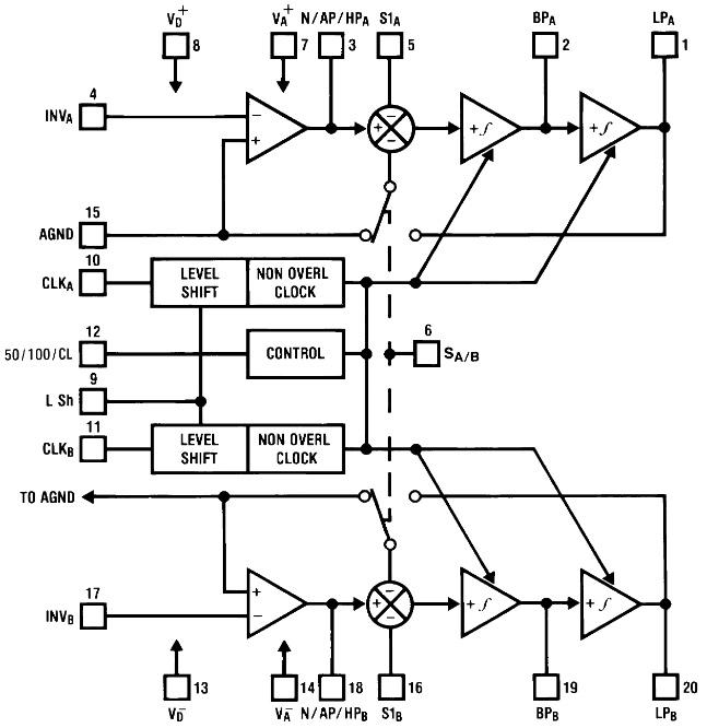
The block diagram below shows how the filter is represented in the MF10 datasheet.6 The diagram is similar to the diagram above, with three op-amps. However, the summing circuitry has been separated out. Moreover, the feedback paths are not shown explictly. Instead, resistors are connected between the chip's external pins (squares) to configure the filter as desired. The mode switch at the top allows the low-pass feedback to be controlled by an external pin (SA/B).

Block diagram of one of the filter sections. Adapted from the datasheet.

Block diagram of one of the filter sections. Adapted from the datasheet.

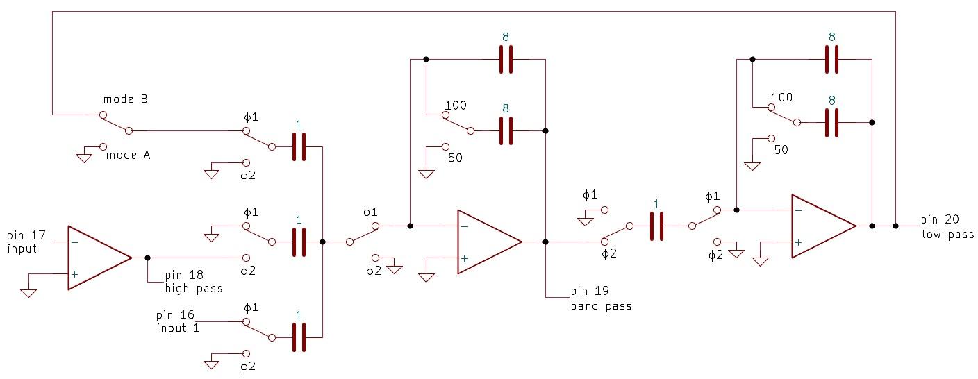
The schematic below is my reverse-engineered schematic of the filter, as implemented on the chip. It closely matches the block diagram, but fills in the details. In the block diagram, the summing circuit (circle) adds one signal and subtracts two signals. This summing circuit is implemented with the three switched capacitors on the left, which act as summing resistors. Note that one switch is grounded during phase 1, while the others are grounded during phase 2; switching the polarity implements addition versus subtraction. The top sum input is either feedback from the low-pass output or ground, selected by an input pin. A CMOS switch is used here, but the switch is static, not clocked, so it doesn't use protection rings and shielding like the other switches.

My reverse-engineered schematic of one of the filters. Click this image (or any other) for a larger version.

My reverse-engineered schematic of one of the filters. Click this image (or any other) for a larger version.

The integrators have switched capacitors on the inputs, acting as resistors. The integration capacitor is either 8 or 16 "squares" of capacitance, selected by a ratio selection pin. This controls the ratio between the clock frequency and the filter frequency, either 50:1 or 100:1.7 Although the integration capacitors are attached to a CMOS switch, the switch is static, so the capacitors act as regular capacitors, not switched capacitors.

The op-amps

The op-amps are fairly standard CMOS op-amps, built from about 35 transistors. (You might get a lower count if you try counting the transistors below, since some of the blocks are multiple transistors.) The op-amp transistors are much larger than the CMOS switch transistors (very bottom, center). On the die, each op-amp is split into two parts: the differential amplifier on the left and an additional amplification stage on the right. A large capacitor (pinkish) sits between the halves. My first thought was that this was the integration capacitor, but it is just a frequency compensation capacitor, common in many op-amps to stabilize the output. The op-amps also have large transistors next to the output pins; these transistors are functionally part of the op-amps, but located next to the pins to minimize resistance.

One of the chip's op-amps. I removed the metal layer to make the transistors visible.

One of the chip's op-amps. I removed the metal layer to make the transistors visible.

One unusual feature of the op-amps is a low-power mode. Pulling a particular IC pin low causes the chip to stop filtering and enter a low-power mode, reducing power consumption by 70%. This is implemented by shutting down the "current mirror" circuits that provide fixed currents to the op-amps and other parts of the chip.

The non-overlapping clock generator

The MF10 chip is driven by external clock signals, one for each filter, with the frequency of the filter proportional to the clock frequency. The photo of the CMOS switches earlier showed that the clock drives four control lines for the switches. You might think that two control lines would be sufficient: the clock and the inverted clock. The problem is that it is very important to avoid having both switches closed at the same time, even for a moment, as that will short the inputs and corrupt the signals. Instead, the two switches have separate control lines that enforce a small gap between when one switch opens and the other one closes. This is implemented with the circuit below that takes an input clock signal and produces the four outputs that drive the switches.

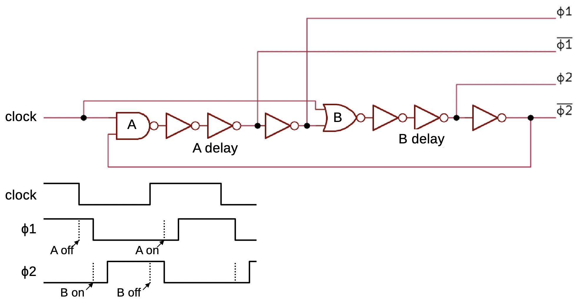
The circuit to generate non-overlapping clock signals. There is a delay between when gate A or B turns on and when the corresponding output changes.

The circuit to generate non-overlapping clock signals. There is a delay between when gate A or B turns on and when the corresponding output changes.

The idea behind the circuit is that a phase is blocked from going high until after the other phase goes low, with a pair of inverters providing additional delay. In more detail, suppose the input clock drops from high to low. Gate A will turn off, causing the phase 1 output (ϕ1) to drop after a few gate delays (A delay). Gate B can't turn on until ϕ1 goes low. After additional gate delays, ϕ2 goes high. The behavior is similar when the input clock goes high. Gate B turns off, causing ϕ2 to go low after a delay. This allows gate A to turn on, turning on ϕ1 after more delay. To summarize, after a phase is turned off, there is a delay before the other phase turns on, so the two phases never overlap.

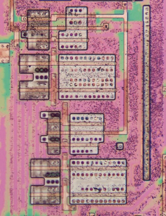
The clock-shaping circuitry is implemented with CMOS logic gates.

The clock-shaping circuitry is implemented with CMOS logic gates.

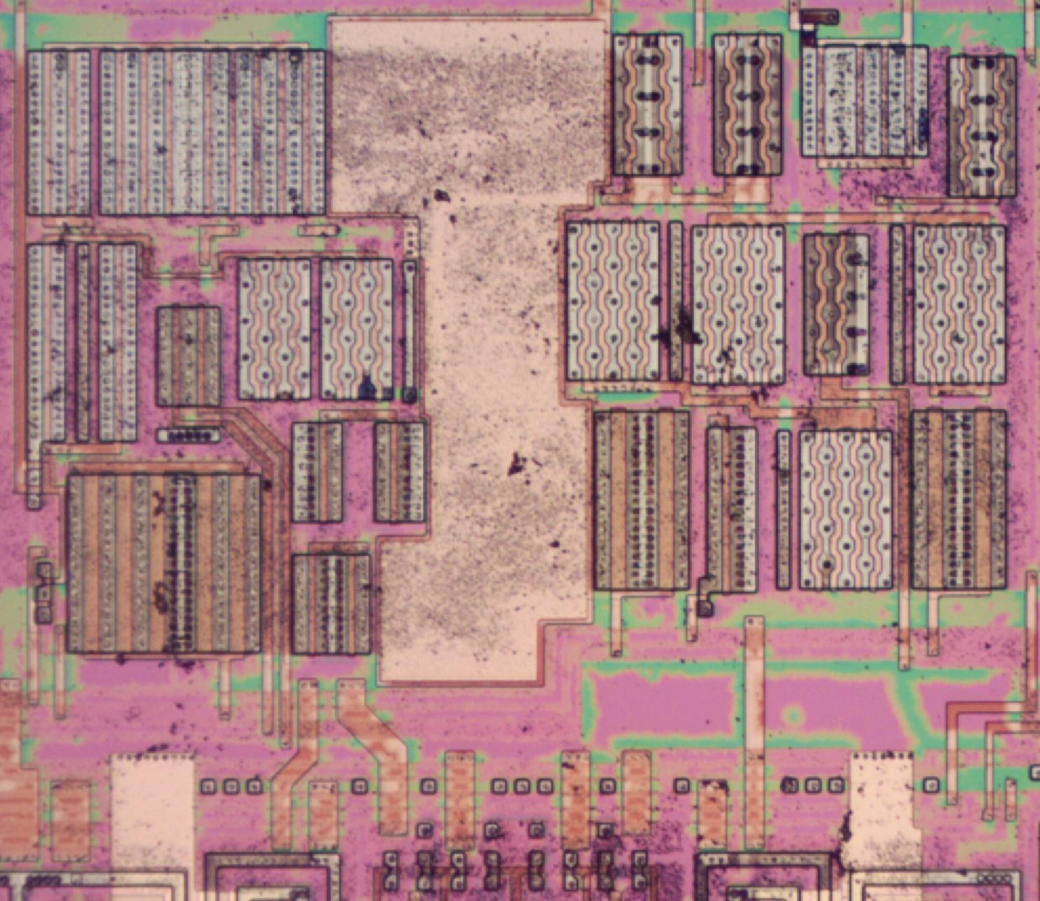
The photo above shows this circuitry under the microscope, with the metal layer removed. The rectangular blocks are doped silicon that forms transistors. The darker regions on the left are NMOS transistors and the lighter regions on the right are PMOS transistors. A CMOS gate consists of NMOS and PMOS transistors working together. The PMOS transistors are larger because PMOS transistors are slightly less efficient than NMOS transistors. The dark circles are contacts between the silicon and the metal layer on top. The copper-colored lines are not metal but a special type of silicon called polysilicon. When a polysilicon line crosses doped silicon, it forms the gate of a transistor. The pinks and greens are due to thin-film interference from a thin layer of oxide that didn't completely dissolve; the silicon is actually gray.

The ternary input

A weird feature of the chip is the input pin that selects the ratio between the input clock and the filter frequency. In effect, this is a digital input with three values. Tying the pin to the high supply voltage selects a 50:1 ratio. Tying the pin to the midpoint between the supply voltages selects a 100:1 ratio. Pulling the pin to the low supply voltage stops the filter and puts the chip into a low-power mode.8

To handle the three-level input, the input goes through two separate buffers, one that transitions at a lower voltage and one that transitions at a higher voltage. Thus, the two buffers separate the middle signal level. Each buffer consists of a special inverter feeding into a regular inverter.

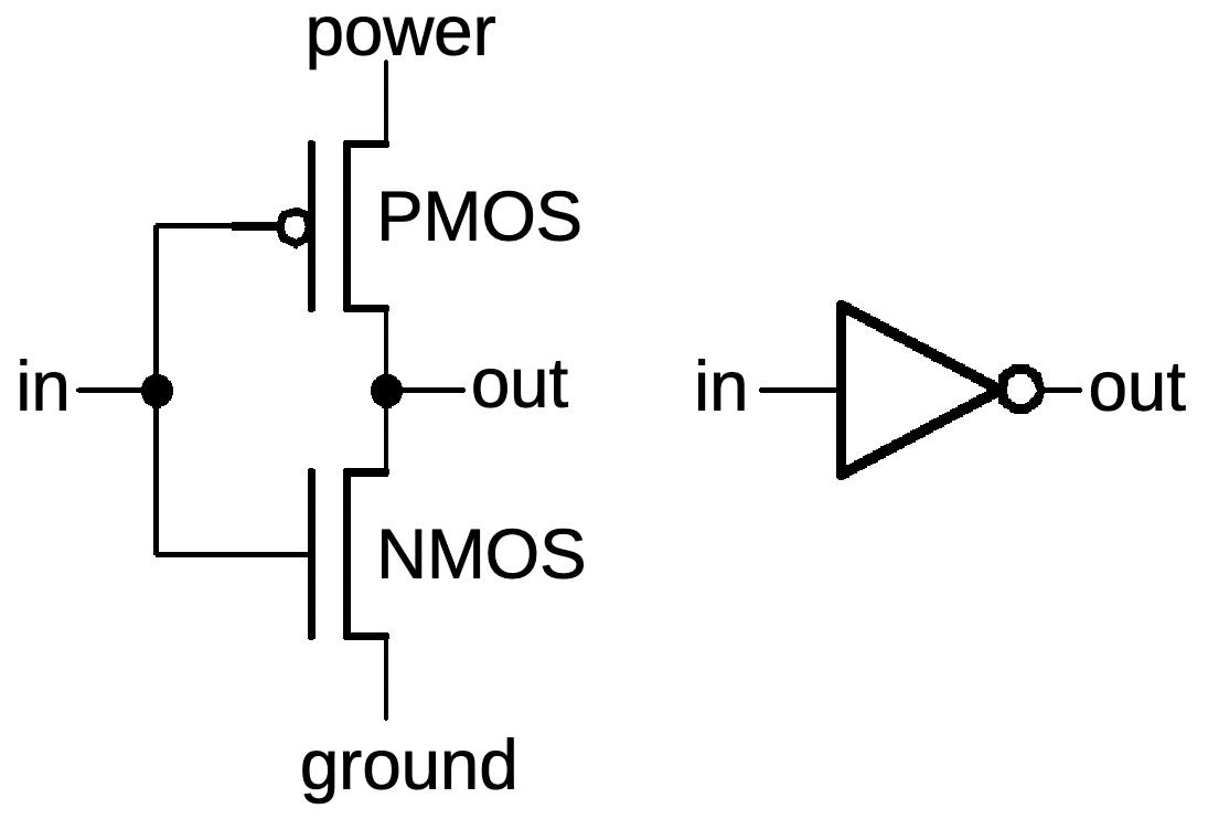
Before explaining the special inverters, I'll review how a regular CMOS inverter works. A CMOS inverter is constructed from a PMOS transistor and an NMOS transistor. When the input is high, the NMOS transistor turns on and pulls the output to ground. When the input is low, the PMOS transistor turns on and pulls the output high. Thus, the input signal is inverted.

A CMOS inverter is constructed from a PMOS transistor and an NMOS transistor.

A CMOS inverter is constructed from a PMOS transistor and an NMOS transistor.

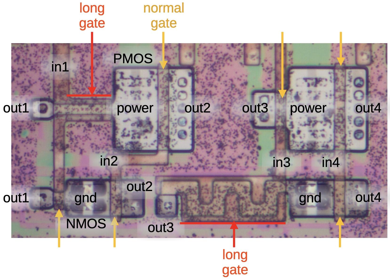
In the die photo, you can see the four PMOS transistors (light gray) and four NMOS transistors (darker), forming four inverters. When a polysilicon line (copper-colored) crosses a doped silicon region, it forms the gate of a transistor. For this picture, I dissolved the metal layer in acid so the transistors are visible. The metal layer connected the transistors to complete the wiring of the inverters: it connects the two "out1" contacts to "in2" and connects the two "out2" contacts to the rest of the chip. For the second buffer, "out3" connects to "in4" and so forth.

The four inverters that handle the ternary input. I flipped the image to make the orientation better.

The four inverters that handle the ternary input. I flipped the image to make the orientation better.

In this circuit, the length of the transistor gates is varied to make the inverters activate at different voltage levels. Six of the transistor gates are normal (orange arrows); the PMOS gates are wider (in the vertical direction) than the NMOS gates because PMOS transistors are inherently weaker. However, two of the transistor gates are unusually long (horizontal direction, red), making the transistors weak since the current must travel a longer distance. The inverter on the left has a weak PMOS transistor. If the input is high or low, the inverter will operate normally. But if the input is in the middle, both transistors will partially turn on. Since the PMOS transistor is very weak, the NMOS transistor will "win", pulling the output low. Thus, the leftmost inverter treats a medium-level input as a 1, outputting a 0. The third inverter is the opposite; the NMOS transistor has a long, winding gate, so it is weak. In this case, a medium-level input will partially turn on both transistors, but the PMOS transistor will "win", pulling the output high. To summarize, the two inverters have opposite behavior for a middle-level signal, allowing the three input levels to be distinguished. Since the output from a special inverter may be weak, the output goes to a normal inverter to amplify the signal.

Conclusions

Like most semiconductor companies, Harris has a complicated history. Harris started way back in 1895 as a printing press company. Harris moved into high technology in the 1950s and 1960s, acquiring various radio and electronics companies. In particular, Harris entered the IC business in 1967, when it acquired Radiation, Inc., renaming it Harris Semiconductor a few years later. (We've encountered some Radiation modules in Apollo systems, but I haven't written about them yet.) Harris got out of the semiconductor business in 1999, spinning off Intersil, which was later acquired by the Japanese semiconductor firm Renesas. In 2019, Harris merged with L3 Technologies to become L3Harris, the eighth-largest defense contractor in the US.

As for switched-capacitor filters, they have lost popularity as filtering is now more easily done in the digital domain. Texas Instruments acquired National Semiconductor (and the MF10) in 2011; TI's website shows the MF10 as active but expensive and out of stock, so it's probably no longer being manufactured. State variable filters are still used in the synthesizer world both because of their flexibility and because they provide low-pass, band-pass, and high-pass filters in one unit.

For more, follow me on Bluesky (@righto.com), Mastodon (@[email protected]), or RSS. Thanks to CuriousMarc for providing the IC. AI statement: Despite the presence of the em dash, no AI was used in the writing of this article (details).

Notes and references

  1. Once we found the "HF-10" part number, a search turned up a National Semiconductor databook that confirmed that the Harris HF-10 was a direct replacement for the National Semiconductor MF10. As for the label "F1-10-5", it turns out that Harris includes the logo in the part number; "HF1-10-5" is the full Harris part number. ↩

  2. You might wonder why the larger capacitors are formed by connecting eight smaller capacitor squares, rather than making one capacitor that is eight times as big. The reason is to get better matching between the two capacitor sizes. A capacitor that is eight times as large won't have exactly eight times the capacitance due to factors such as the behavior of the electric field around the edge of the capacitor, inaccuracies that may make the capacitor slightly larger or smaller than desired, or etching variability around the edges. By building larger capacitors out of identical smaller capacitors, the values can match very well, up to ±0.01% according to The Art of Analog Layout. (With laser trimming, matching of ±0.001% is possible, but that is much more accuracy than the MF10 required.) ↩

  3. Most chips from this era have a single layer of polysilicon, so I was surprised to find two layers in this chip. I've seen two layers of polysilicon before, in the MK4116 DRAM chip and AMD's LANCE Ethernet chip. In both cases, the second layer of polysilicon was used for storage devices. ↩

  4. A standard op-amp integrator is an inverting integrator, and the output is negative. However, the MF10 uses the four-switch switched capacitor that inverts the input voltage. The two negatives cancel out, so the MF-10's integrator is a non-inverting integrator. See Introducing the MF10: A Versatile Monolithic Active Filter Building Block for details. ↩

  5. To remove the metal layer, I used Whink rust stain remover (1.5-3.5% HF) to remove the oxide layer and hydrochloric acid to dissolve the metal. I applied Whink for 20 minutes and HCl for 16 minutes in total. I alternated each chemical for about 3 minutes each, applying a few drops at a time. I examined the die under the microscope after each application to gauge the progress.

    I stopped at this point since the metal was removed and the underlying transistors were visible. Moreover, the silicon became differentially stained, with NMOS transistors significantly darker than PMOS transistors. Some more Whink would probably improve the appearance of the die, but the risk is that the polysilicon might get removed, which would be bad for reverse engineering. In other words, I'd rather stop too early than destroy the features that I want to see. ↩
  6. For reference, the full block diagram of the chip is below, from the datasheet.

    Block diagram of the MF10 from the Texas Instruments datasheet.

    Block diagram of the MF10 from the Texas Instruments datasheet.

     ↩

  7. The filter frequency of the MF10 can be set to either the clock frequency divided by 50 or divided by 100. You might wonder where these ratios come from, since the capacitors on the chip are in 8:1 or 16:1 ratios, not 50:1 or 100:1. The formula for a switched-capacitor integrator is that the filter frequency is the clock frequency divided by 2Ï€ times the capacitor ratio. (This can be derived from the op-amp integrator formula and the equivalent resistance of a switched capacitor.) It turns out 2Ï€×8 is 50.27 and 2Ï€×16 is 100.5, providing the 50 and 100 values.

    Note that these values aren't exactly 50 and 100; they are off by 0.5%. Curiously, the datasheet specifies that the typical frequency error is ±0.2%, significantly smaller. I suspect that the explanation is that the capacitor ratio is not precisely 16:1, due to stray capacitance in the wiring and other factors, and the designers ensured that these factors tweaked the ratio in the desired direction. ↩

  8. I suspect that the ternary input pin was used because the chip didn't have enough physical pins for all the functions they wanted. Note that the two filters are entirely independent, even with separate clocks, except for the 50/100 ratio control and the A/B mode control. I'm sure that these two functions would have independent control pins if the chip had pins available. They could have used a standard 24-pin package for the chip rather than the somewhat unusual 20-pin package, but maybe they had a motivation for avoiding a much larger 24-pin package. ↩

Reverse-engineering the vintage Intel 8087's tangent algorithm: more than CORDIC

I hope you're not tired of the 8087, because I have another article about Intel's floating-point chip.1 In 1980, Intel introduced the 8087, making floating-point operations much faster in the IBM PC and other systems. In this article, I look at the algorithm behind the chip's tangent instruction. One popular approach for trigonometric functions is an algorithm called CORDIC. Another approach is a polynomial approximation. The 8087 combined the two to obtain both high accuracy and high performance. The 8087 provided an enormous speedup over the 8086 microprocessor, computing a tangent in 90 microseconds rather than 13,000 microseconds.2

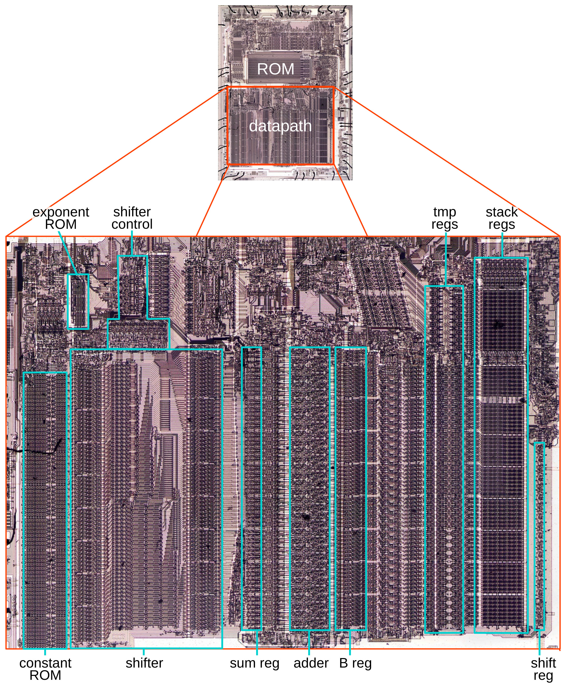
By examining the circuitry and microcode of the 8087, I can explain the algorithm behind the tangent instruction, called FPTAN. To explore the 8087's circuitry, I popped the lid off a chip with a chisel and created a high-resolution image with a microscope. The microcode ROM is the large rectangular region in the center of the die, holding the 1648 micro-instructions that control the chip. The bottom half of the chip (red box) is the datapath, the circuitry that performs floating-point calculations on 80-bit values.3

A close-up of the 8087's datapath, showing functional blocks that are used by FPTAN. Click this image (or any other) for a larger version.

A close-up of the 8087's datapath, showing functional blocks that are used by FPTAN. Click this image (or any other) for a larger version.

Zooming in on the datapath shows the relevant functional units. The exponent ROM holds fixed exponent values that the algorithms need. The constant ROM holds constants, including the constants used by the CORDIC algorithm. The shifter is a large component; it shifts a 64-bit value left or right by arbitrary amounts. The adder is the heart of the 8087's calculations; as well as providing addition and subtraction, it is used in a loop for multiplication, division, and square roots. The B register holds one input to the adder, while multiple sources can provide the other input. The sum register holds the adder's output. The eight stack registers and the temporary registers hold floating-point numbers. Finally, the shift register holds 16 status bits for the CORDIC calculations.

The CORDIC algorithm

CORDIC is a clever algorithm for quickly computing transcendental functions with simple hardware: it uses shift and add instructions along with table lookups, but doesn't need multiplication or division. This algorithm dates back to 1956, when it was developed for the B-58 Hustler, the first bomber capable of flying at Mach 2. The aircraft had an analog navigation computer, but analog components provided limited accuracy. Engineer Jack Volder was given the task of designing a digital computer to replace the analog computer.7 One key problem was that an analog computer can easily generate sines and cosines with an electromechanical device called a resolver. But trigonometric functions are difficult to produce digitally, especially with the slow transistors of that era.

A Convair B-58A Hustler, on display in San Antonio, TX (details).

A Convair B-58A Hustler, on display in San Antonio, TX (details).

Jack Volder came up with a fast way to calculate trigonometric functions with simple hardware. He called the algorithm—and the computer that implemented it—CORDIC: "COordinate Rotation DIgital Computer". CORDIC converts an angle to a vector, where the vector's coordinates provide the necessary trig functions. The trick is to break down the angle into a sequence of special angles, angles that make vector rotation easy. These special angles are precomputed and stored in a table, so the CORDIC calculation can be performed quickly, even on 1950s hardware. Each CORDIC iteration provides an additional bit of accuracy, so the algorithm converges rapidly. CORDIC became popular, including in scientific calculators, which used decimal CORDIC instead of binary.

Some trigonometry

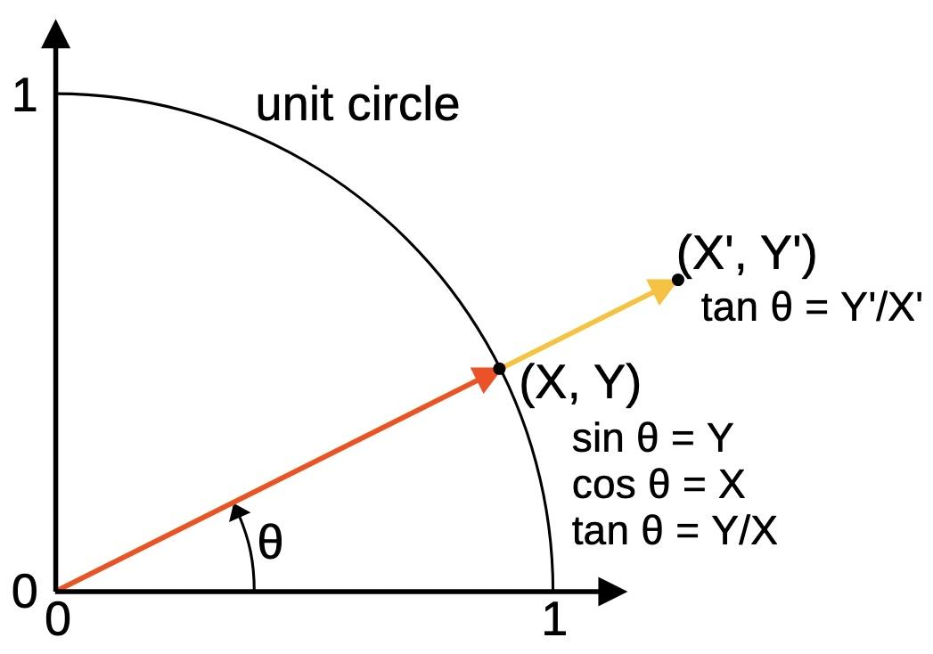
I'll try to keep the math to a minimum, but in this section I'll give a quick explanation of how CORDIC works. The diagram below reviews how trig functions are related to the coordinates of a point. Suppose you have an angle θ; it specifies a point (X, Y) on the unit circle. The basic formulas are X=cos θ, Y=sin θ, and Y/X = tan θ. Thus, if you can determine the coordinate (X, Y), then you can determine the value of the trig functions. If the point is not on the unit circle, e.g. (X', Y'), then you can still easily determine tan θ. (Spoiler: this is what the 8087 does.) However, sin θ and cos θ become messy.4

The relationship between an angle, the X and Y coordinates, and the trig functions.

The relationship between an angle, the X and Y coordinates, and the trig functions.

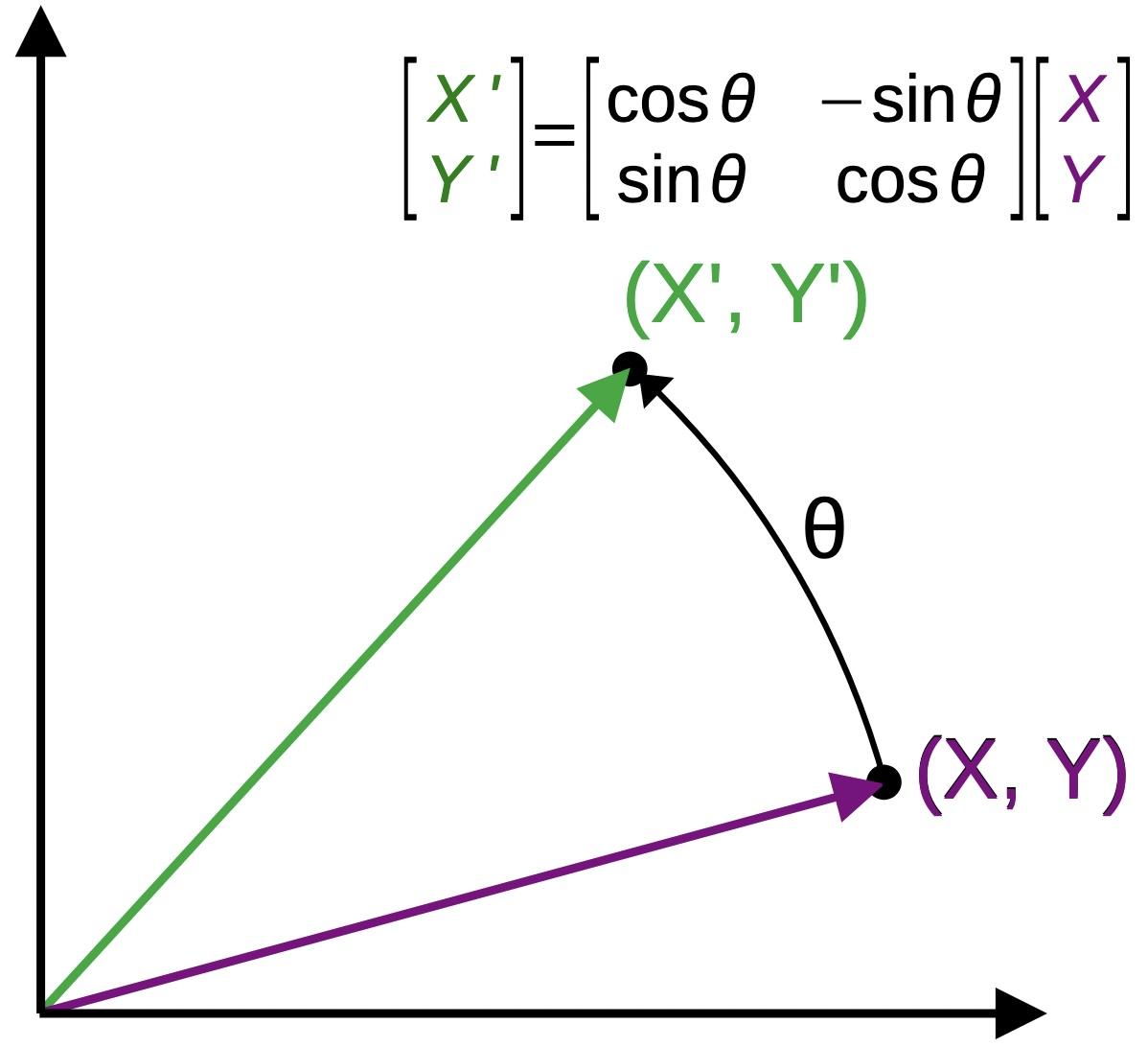
If you've done any computer graphics, you've probably seen how a rotation matrix can rotate a point by an angle. (If you're not familiar with rotation matrices, you can read about them here or just trust that it works.) Multiplying a point (X, Y) by the rotation matrix yields the new point (X', Y') as shown below.

A point can be rotated by using a rotation matrix.

A point can be rotated by using a rotation matrix.

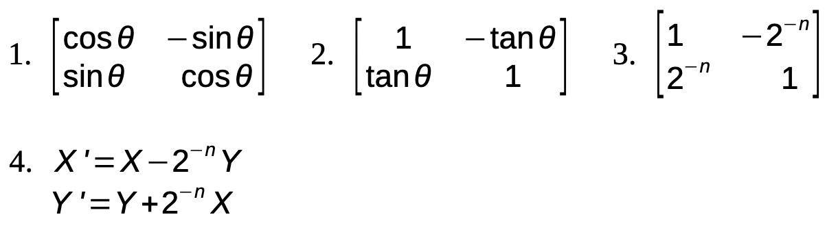
Unfortunately, since the rotation matrix (1, below) requires sin and cos, it doesn't seem like it helps solve our problem. However, we can divide the matrix by cos θ; this seems even less helpful since now the matrix (2) needs tan, which is what we want to evaluate. (Moreover, the vector's length will grow.) But the key to CORDIC is to use special angles, αn = arctan(2-n). When we substitute one of these special angles into the matrix, we get matrix (3), which is easy to evaluate in hardware: multiplying by a power of 2 can be done by shifting the bits.

Simplifying the rotation matrix.

Simplifying the rotation matrix.

Applying matrix (3) to the point (X,Y) gives the equations (4). These are key equations for the CORDIC process. The important thing is that these equations are fast and easy to compute in machine language or hardware, as the only operations are addition, subtraction, and binary shifting.

With that background, we can see how CORDIC works. First, we break down the desired input angle into a combination of special angles that adds up to the desired angle.5 Then we apply the rotation formula above for each special angle, starting with the unit vector (1, 0). The result is a point (X, Y) at the desired angle, and then the desired tangent is simply Y/X.6 Since the table of special angles is precomputed, the arctan operations don't slow down the process. As an aside, after the first few terms, the special angles approach 2-n, so they shrink by roughly a factor of 2 at each step.

To summarize, the CORDIC algorithm consists of looping through a table of stored angles. If the stored angle is less than the desired angle, the stored angle is subtracted from the desired angle to yield a new desired angle and the equations above (shifts, add, and subtract) are applied to yield a new vector. At the end, the tangent of the original angle is given by Y/X.

The rational polynomial approximation

The accuracy of CORDIC depends on the number of terms that are used. With 16 terms, the accuracy is approximately 2-16, or 16 bits of accuracy. To get 64 bits of accuracy would require calculating 64 terms (and a table of 64 special angles). To get an answer faster, the 8087 uses 16 bits of CORDIC and uses another algorithm for the remaining angle. (The remaining angle is the gap between the sum of special CORDIC angles and the desired angle, so it is very small, around 2-16.)

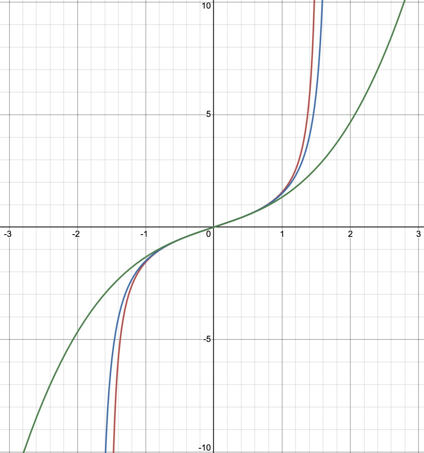
For the remaining angle, the 8087 uses a Padé approximant, which is the ratio of two polynomials. There's a whole family of Padé approximations, depending on the order of the polynomials. The 8087 uses a simple formula: 3x/(3-x2).8 Although this approximation is simple, it is very accurate for small values; its error is proportional to x4. Since x<2-16, the error will be less than 2-64, meeting the 64-bit accuracy requirement for the 8087. Moreover, the 8087 doesn't need to perform the division in the rational polynomial since FPTAN returns a separate numerator and denominator. Thus, the division is "free".

The tangent function (red), rational approximation (blue), and Taylor series (green).
Disclaimer: The Taylor series isn't as bad as it appears, since the relevant range is very close to 0.
Graph generated with Desmos.

The tangent function (red), rational approximation (blue), and Taylor series (green). Disclaimer: The Taylor series isn't as bad as it appears, since the relevant range is very close to 0. Graph generated with Desmos.

If you've studied calculus, you might think that a Taylor series polynomial is the way to go, but the ratio of two polynomials is better. (One reason is that tangent blows up to infinity at π/2. A polynomial won't blow up, but the ratio of polynomials can, so it fits the tangent function better.) The graph above compares the tangent function (red), the rational approximation (blue), and the third-order Taylor series (green).

Putting the pieces together: the 8087 algorithm

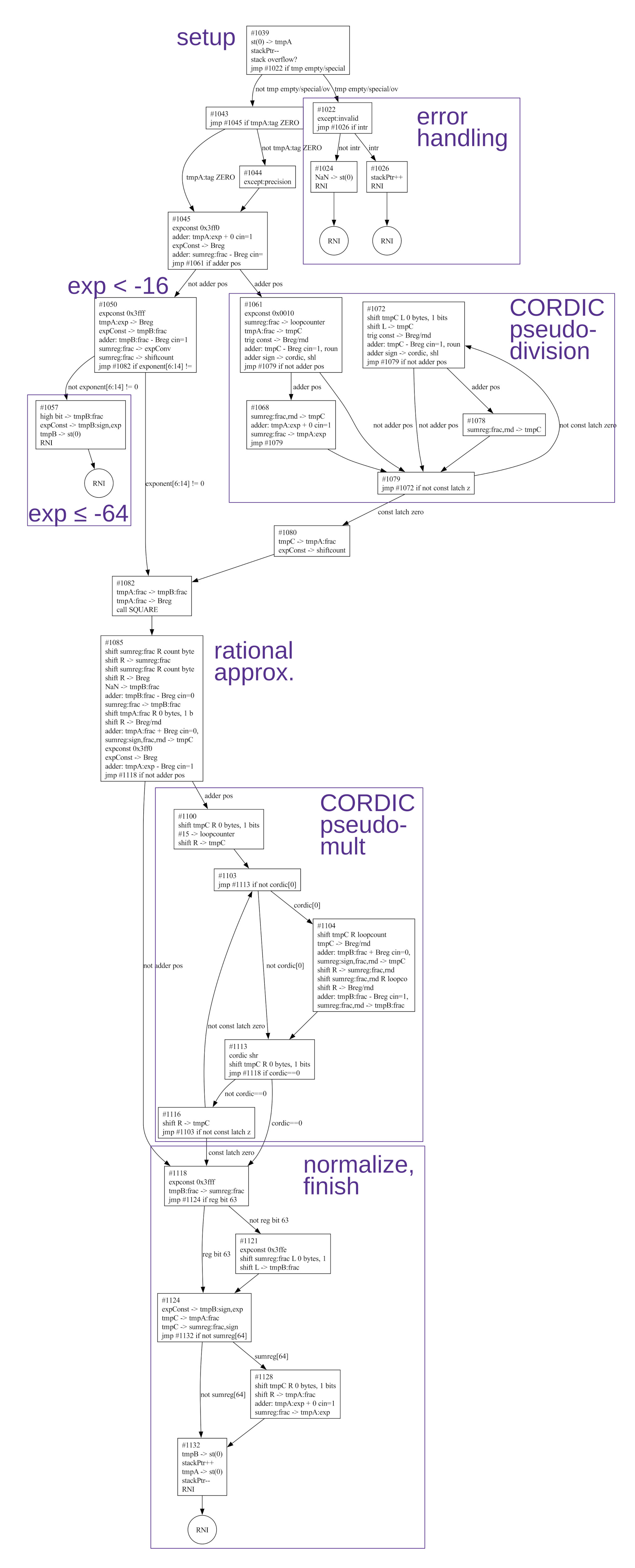
The 8087's tangent algorithm has three parts: determining the CORDIC decision bits (called pseudo-division), computing the rational approximation, and applying the rotation equations based on the CORDIC decision bits (called pseudo-multiplication).9

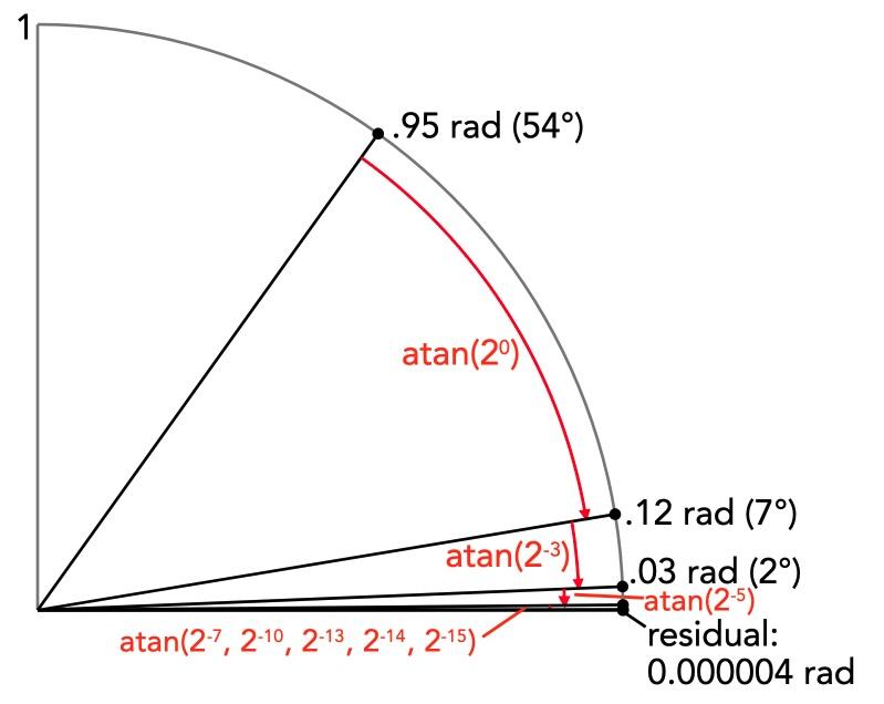
In more detail, the first step determines which special angles to add to approximate the input angle. Each special angle is compared to the remaining input angle and subtracted if it is smaller. If the angle is subtracted, a 1 is recorded; otherwise, a 0 is recorded. Since this process is similar to how long division subtracts (or doesn't subtract) successive shifted versions of the divisor, generating 1s or 0s for the quotient, the process is known as pseudo-division. Note that the rotations are not applied in this step. Instead, this step decides which rotations to apply later.

The diagram below shows this process applied to the input angle 0.95 radians.10 The process generates the sequence of bits [1,0,0,1,0,1,0,1,0,0,1,0,0,1,1,1], where the leftmost bit indicates arctan(20) and so forth. The angle is reduced by roughly a factor of 2 at each step, so the residual angle is very small.

In the first phase of the CORDIC algorithm—pseudo-division—the input angle is reduced by special angles, leaving a residual angle at the end. ("rad" is radians, not the unit of radiation.)

In the first phase of the CORDIC algorithm—pseudo-division—the input angle is reduced by special angles, leaving a residual angle at the end. ("rad" is radians, not the unit of radiation.)

Next, the tangent of the remaining angle is calculated with the rational approximation function, 3x/(3-x2). The result is used as the initial vector for the next step. The division is not performed here; instead, the numerator becomes Y in the initial vector and the denominator becomes X. Thus, the expensive division step is avoided, since it happens implicitly in the answer. Multiplying by 3 is easy (shift left and add), so the only expensive operation at this step is squaring the angle, which requires a full 64-bit multiplication.

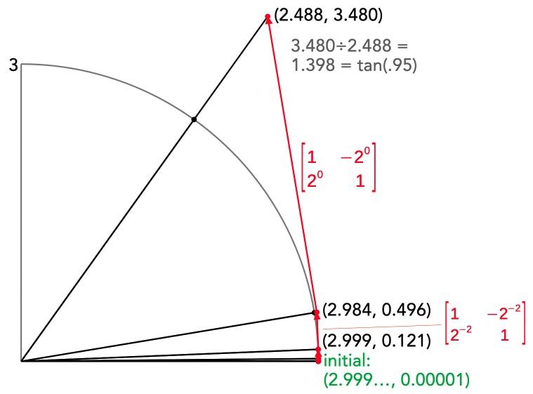
The final step applies each CORDIC rotation if the corresponding decision bit from the first step is 1. Since this is somewhat analogous to binary multiplication, which adds the multiplicand at each step if the multiplier bit is 1, this step is known as pseudo-multiplication. As described earlier, each rotation is computed with shifts, addition, and subtraction, so each rotation is inexpensive. Each rotation in this step corresponds to an angle reduction in the first step. The rotations are applied in reverse order—the smallest one first—to reduce rounding error. To accomplish this, the decision bits are stored in a 16-bit shift register in the first step, and shifted out in opposite order in this step.

In the last phase of the CORDIC algorithm—pseudo-multiplication—a vector is rotated multiple times by applying shifts and adds. The final vector provides the tangent.

In the last phase of the CORDIC algorithm—pseudo-multiplication—a vector is rotated multiple times by applying shifts and adds. The final vector provides the tangent.

The diagram above shows the process applied to the input 0.95. The initial vector (green) comes from the rational approximation function; it is very close to (3, 0), but slightly rotated due to the tiny residual angle. Each rotation step generates a new vector that matches the angle from the corresponding step in the first part; I show two of the rotation matrices. Note that the vectors diverge from the circle—a consequence of dividing each matrix by cos θ—but this doesn't affect the tangent.

The FPTAN instruction is somewhat peculiar as it doesn't return the tangent directly. Instead, it returns the Partial Tangent: the two coordinate values (X and Y) that can be divided to produce the tangent. One might wonder why the chip didn't do the division automatically. The motivation was that division was slow back then, and omitting the division allowed for optimizations in some cases.

Relevant hardware details of the 8087

In this section, I'll explain some features of the 8087 that are important for the microcode implementation of FPTAN.

The 8087 supports a variety of data types, but internally, everything is stored as an 80-bit floating-point number called a "temporary real". A number has three parts: a sign bit, a 15-bit exponent, and a 64-bit significand (the fractional part), In most cases, a floating-point number is represented by sign × significand × 2exponent. The advantage of floating-point numbers is that the exponent allows them to cover a huge range, from very small to very large. The significand is a 64-bit binary number of the form 1.bbb…: a leading 1, followed by the binary point (the binary equivalent of the decimal point) and the rest of the bits.11 One important detail is that the exponent is stored with a "bias" of 16383 added to it. Thus, the stored exponent is always positive, even if the real exponent is negative. For instance, an exponent of 1 is stored as 0x4000, and an exponent of -16 is stored as 0x3fef.

The 80-bit temporary real format and the register formats. The dot indicates the binary point, analogous to the decimal point.

The 80-bit temporary real format and the register formats. The dot indicates the binary point, analogous to the decimal point.

To use the 8087, a programmer stores values in its eight internal registers, organized as a stack. Each register holds an 80-bit floating-point number. To optimize performance, each value in the register stack also has an associated "tag" value: zero, valid, special, or empty. A value of zero is tagged as zero. A "normal" floating-point value is tagged as valid. If the value is infinity, Not a Number (NaN), or a denormalized value, then it is tagged as special. Finally, an empty tag indicates that a register does not hold a value; this allows detection of stack underflow (reading an empty register) or stack overflow (storing to a non-empty register).

The 8087 also has temporary registers that it uses internally: tmpA, tmpB, and tmpC. (These registers are heavily used for the tangent calculation.) tmpA and tmpB are 80-bit registers, along with two tag bits. However, tmpC is different: it doesn't have a sign, exponent, or tag. Moreover, the significand is 68 bits; tmpC has an additional bit to prevent overflow and three additional low-order bits for rounding, known as guard, round, and sticky.

In the microcode, each 16-bit micro-instruction performs one low-level operation. Many of the operations move data from one register to another. Other operations provide conditional jumps, subroutine calls, and returns. A bit shift operation takes two micro-instructions: the first moves a value to the shifter and configures the direction and amount of shift. The second micro-instruction (which may be a distance after the first) moves the result from the shifter to a destination.

Similarly, addition takes two micro-instructions. The first micro-instruction specifies the first argument to add and selects various options such as carry and rounding. (For subtraction, an option complements the second argument.) The second argument always comes from the B register, which confusingly is unrelated to the tmpB register. The second micro-instruction moves the result from the sum register to a destination.

Implementation of the tangent algorithm in microcode

In this section, I'll discuss some highlights of the tangent microcode. The listing below shows the 8087's microcode, along with my comments. Each line indicates a 16-bit micro-instruction. The control flow is a bit complicated, so I've put a flowchart in the footnotes.12

FPTAN:
#1039 st(0) -> tmpA        store argument in tmpA
#1040 stackPtr--           check if room on stack to push result
#1041 stack overflow?
#1042 jmp #1022 if tmp empty/special/overflow/div exit if bad argument or stack overflow
#1043 jmp #1045 if tmpA:tag ZERO is argument 0?
#1044 except:precision     precision exception except for 0
#1045 expconst 0x3ff0      Test if exponent >= -16
#1046 adder: tmpA:exp + 0 cin=1 argument exponent + 1
#1047 expConst -> Breg
#1048 adder: sumreg:frac - Breg cin=1 subtract -15
#1049 jmp #1061 if adder pos CORDIC if exponent >= -16
#1050 expconst 0x3fff      non-CORDIC path:
#1051 tmpA:exp -> Breg     check original exponent
#1052 expConst -> tmpB:frac against exponent 0
#1053 adder: tmpB:frac - Breg cin=1 subtract
#1054 sumreg:frac -> expConv 3fff - exp (i.e. -exp unbiased)
#1055 sumreg:frac -> shiftcount
#1056 jmp #1082 if exponent[6:14] != 0 if exp > -64 goto rational approximation
#1057 high bit -> tmpB:frac otherwise return original argument
#1058 expConst -> tmpB:sign,exp push 1 for X (denom): result is orig angle
#1059 tmpB -> st(0)
#1060 RNI
#1061 expconst 0x0010      CORDIC path
#1062 sumreg:frac -> loopcounter loopcounter = exp + 16
#1063 tmpA:frac -> tmpC    tmpC = original angle
#1064 trig const -> Breg/rnd
#1065 adder: tmpC - Breg cin=1, roundmode subtract first CORDIC angle
#1066 adder sign -> cordic, shl save bit  in shift register
#1067 jmp #1079 if not adder pos
#1068 sumreg:frac,rnd -> tmpC
#1069 adder: tmpA:exp + 0 cin=1 increment exp if first angle used
#1070 sumreg:frac -> tmpA:exp
#1071 jmp #1079
#1072 shift tmpC L 0 bytes, 1 bits top of CORDIC scan loop
#1073 shift L -> tmpC      shift angle left
#1074 trig const -> Breg/rnd
#1075 adder: tmpC - Breg cin=1, roundmode subtract CORDIC angle
#1076 adder sign -> cordic, shl save decision bit in shift register
#1077 jmp #1079 if not adder pos
#1078 sumreg:frac,rnd -> tmpC
#1079 jmp #1072 if not const latch zero bottom of CORDIC scan loop
#1080 tmpC -> tmpA:frac    update tmpA, tmpB
#1081 expConst -> shiftcount 16 -> shiftcount (otherwise based on exponent)
#1082 tmpA:frac -> tmpB:frac Padé approximation
#1083 tmpA:frac -> Breg    tmpA = ang
#1084 call SQUARE          square the angle
#1085 shift sumreg:frac R count byte bit
#1086 shift R -> sumreg:frac shift twice to scale square
#1087 shift sumreg:frac R count byte bit
#1088 shift R -> Breg      Breg = ang^2
#1089 1.1 -> tmpB:frac     3 (with exp 1)
#1090 adder: tmpB:frac - Breg cin=0
#1091 sumreg:frac -> tmpB:frac tmpB (X) = 3-ang^2
#1092 shift tmpA:frac R 0 bytes, 1 bits
#1093 shift R -> Breg/rnd
#1094 adder: tmpA:frac + Breg cin=0, roundmode ang + ang/2
#1095 sumreg:sign,frac,rnd -> tmpC tmpC (Y) = 3×ang with appropriate exponent
#1096 expconst 0x3ff0      exponent -15
#1097 expConst -> Breg
#1098 adder: tmpA:exp - Breg cin=1
#1099 jmp #1118 if not adder pos skip if exponent too small
#1100 shift tmpC R 0 bytes, 1 bits CORDIC pseudo-multiplication path
#1101 #15 -> loopcounter
#1102 shift R -> tmpC
#1103 jmp #1113 if not cordic[0] CORDIC: if saved decision bit...
#1104 shift tmpC R loopcount send tmpC (Y) to shifter
#1105 tmpC -> Breg/rnd     send tmpC to adder
#1106 adder: tmpB:frac + Breg cin=0, roundmode tmpB (X) not shifted because tmpC scaled
#1107 sumreg:sign,frac,rnd -> tmpC tmpC = tmpC + tmpB (implicit >>n)
#1108 shift R -> sumreg:frac,rnd shifted old tmpC to sumreg
#1109 shift sumreg:frac,rnd R loopcount shift right again because tmpC scaled
#1110 shift R -> Breg/rnd  and send to B reg
#1111 adder: tmpB:frac - Breg cin=1, roundmode
#1112 sumreg:frac,rnd -> tmpB:frac tmpB = tmpB - tmpC>>n
#1113 cordic shr           shift out shift register bit
#1114 shift tmpC R 0 bytes, 1 bits start shift of tmpC (Y)
#1115 jmp #1118 if cordic==0 done if shift register empty
#1116 shift R -> tmpC      shift tmpC (Y) right
#1117 jmp #1103 if not const latch zero done if counter at zero
#1118 expconst 0x3fff      CORDIC done
#1119 tmpB:frac -> sumreg:frac Test top bit of tmpB (X)
#1120 jmp #1124 if reg bit 63 If set, use exponent 0
#1121 expconst 0x3ffe      Otherwise, use exponent -1 and
#1122 shift sumreg:frac L 0 bytes, 1 bits shift left one bit to normalize
#1123 shift L -> tmpB:frac
#1124 expConst -> tmpB:sign,exp store exponent in tmpB
#1125 tmpC -> tmpA:frac    store tmpC (Y) in tmpA
#1126 tmpC -> sumreg:frac,sign
#1127 jmp #1132 if not sumreg[64] test overflow bit
#1128 shift tmpC R 0 bytes, 1 bits if set, normalize by shifting right
#1129 shift R -> tmpA:frac
#1130 adder: tmpA:exp + 0 cin=1 and increment exponent by 1
#1131 sumreg:frac -> tmpA:exp
#1132 tmpB -> st(0)        tmpB to top of stack: X (denom)
#1133 stackPtr++
#1134 tmpA -> st(0)        tmpA to st(1): Y (numerator)
#1135 stackPtr--
#1136 RNI                  End of FPTAN

The FPTAN microcode starts at address #1039 (decimal). The microcode starts by moving the argument from the top of the stack to the tmpA register. If the top value is empty, this indicates a stack underflow. If the next element on the stack (the position that will hold the result) is not empty, this indicates a stack overflow. In either case, the microcode indicates an "invalid" exception and ends the instruction.

One peculiar feature of the 8087 is that it flags a result with a "precision" exception if the result is not exact. (This happens very frequently, even for, say, 1/10.) The only tangent that the 8087 can compute precisely is tan(0), so all other inputs result in a precision exception (#1044).

Next, the argument's exponent is tested, splitting the execution into three paths. If the exponent is -64 or less, the argument is so small that the tangent equals the argument, within the accuracy of the system.13 In this case (#1057), the original argument is returned unchanged (with the denominator 1 pushed), and the code ends. The second case is if the argument's exponent is -17 or less. In this case, the CORDIC step is skipped, and the routine jumps directly to the rational approximation (#1082).

CORDIC pseudo-division

The most interesting case is the CORDIC path (#1061), taken if the exponent is between -1 and -16. Conceptually, the code performs 16 CORDIC steps, using 16 stored angles. However, the code is optimized, skipping the large angles for smaller inputs. Specifically, the loop counter is initialized based on the exponent of the input angle (#1062). The CORDIC pseudo-division loop (#1061-#1080) tests the angles, subtracting ones that aren't too big.14

The decision results are recorded in a 16-bit shift register, located on the far right side of the die. Presumably, this is where the layout had some unused space. Since the shift register is loaded and unloaded serially, it doesn't need access to the internal fraction bus, just two lines to shift the bits in and out, so the shift register could be located in otherwise unused space.

The code is optimized to use 64-bit integer arithmetic rather than floating-point arithmetic. This makes it tricky to understand the code since values must be viewed more as fixed-point numbers with implicit exponents. These exponents are not stored anywhere, but can be determined by analyzing the algorithm. Even the angle constants in the ROM do not have explicit exponents.15 Moreover, the implicit exponents change for each step through the loop to preserve accuracy. Roughly speaking, each cycle of the loop reduces the values by a factor of 2, and the angle constants shrink accordingly. If the values had a fixed exponent, they would end up with 16 leading zeros, wasting precision. But by scaling the values each cycle (with a left shift), the numbers continue to use the full 64 bits. In other words, the hardware is performing fast integer arithmetic, but mathematically you can think of it as fixed-point with exponents that don't physically exist in the chip. See the table in the footnotes16 for details on how the implicit exponents change through the loop.

Rational polynomial approximation

After the CORDIC pseudo-division loop, the microcode calculates the rational polynomial approximation (#1082). The small-angle path rejoins the execution flow here. The microcode to calculate the polynomial approximation has a few interesting features. The most time-consuming part is the SQUARE routine, which multiplies a fixed-point number by itself. Multiplication is complicated, so I'll give the details in a later post. But in brief, the 8087 uses Booth's Algorithm to multiply by two bits at a time (radix 4), so it is twice as fast as regular binary multiplication. The loop to perform the shifts and adds is implemented in hardware, rather than microcode. That is, one microcode instruction performs 32 additions: the hardware tests the bits, does the appropriate add or subtract, updates the loop counter, and loops. For performance, the shifting is done with specialized shifters, not the 8087's general-purpose shifter.

Except for the square, the polynomials are calculated with additions rather than multiplications. The constant 3 doesn't come from the constant ROM, but from special-purpose transistors that set the top two bits of the significand; this is usually used to supply an NaN. (If the implicit exponent is 1, this corresponds to 3.) Subtracting the square yields the numerator. For the denominator, the angle is shifted right (i.e. divided by 2) and added to itself. This performs a multiplication by 3 (technically by 1.5, but increasing the implicit exponent to 1 turns this into 3). It would be expensive to divide the numerator by the denominator; instead, the numerator and denominator are used as the initial Y and X values for the following CORDIC steps.

CORDIC pseudo-multiplication

Next is the CORDIC loop where the rotations are applied to the vector (#1100). The rotations are applied in the reverse order from how they were computed in the first step: the smallest rotations are applied first to preserve accuracy. Bits are shifted out of the shift register to indicate if the rotation should be applied or not. As soon as the shift register is all zeros, the loop stops. In other words, smaller angles go through the loop just a few times, not the full 16 times.

A close-up of the microcode ROM under the microscope. A transistor is formed where a vertical polysilicon line crosses doped silicon (pink). The 8087's ROM is unusual: it uses four transistor sizes, so it stores two bits per transistor, twice the density of a regular ROM.

A close-up of the microcode ROM under the microscope. A transistor is formed where a vertical polysilicon line crosses doped silicon (pink). The 8087's ROM is unusual: it uses four transistor sizes, so it stores two bits per transistor, twice the density of a regular ROM.

The rotations are applied by shifts and adds (or subtracts), but keeping track of the implicit exponents is a bit tricky. Since the vector starts almost horizontal, the X value is approximately 3, and the Y value is around 2-16. As the vector rotates, X remains roughly 3, but Y potentially increases by a factor of 2 each time. To provide the maximum accuracy for each number, the exponent for X (tmpB) is 1, while the exponent for Y (tmpC) starts off at -14 and increases by 1 each loop as Y is shifted right. (Remember that these exponents are not stored anywhere but are implicit.) Since the two registers have different (implicit) exponents, the values must be shifted before adding. The shift amounts aren't intuitive; the table16 in the footnotes may help clarify.

After the CORDIC loop, the final part of the code (#1118) normalizes the X and Y values, creating the floating-point values that are returned from the instruction. Recall that these aren't "real" floating-point values at this point, so they may need adjustment. Specifically, if X doesn't have a leading 1, it is shifted left one position, while if Y has two leading digits, it is shifted right one position. In either case, the exponent is adjusted accordingly. The X and Y values are put on the stack (#1132) to complete the instruction.

Conclusions

The FPTAN instruction is fairly slow as 8087 instructions go, due to its complexity. The documentation says that it takes typically 450 clock cycles. (The time has a large range; depending on the value, it can take 30 to 540 clock cycles.) For the value I examined (0.95), 33% of the time is in the CORDIC pseudo-division, 15% in the rational polynomial (mostly the squaring operation), 47% in the CORDIC pseudo-multiplication, and 5% overhead.

CORDIC is a popular way to compute trig functions, but there are alternatives such as polynomials. The 8087 is unusual because it combines CORDIC and a rational polynomial. For the Pentium, Intel moved from CORDIC to polynomial approximations; the Pentium's fast multiplication circuitry made polynomials practical. Nowadays, Intel has libraries such as MKL (Math Kernel Library) and Short Vector Math Library (SVML) that provide highly optimized implementations tailored to Intel hardware. These libraries are said to use polynomial approximations, using parallel instructions (SIMD) for performance, rather than specialized hardware. With these libraries, x87 operations and 80-bit floats are mostly obsolete. Nonetheless, I hope you've enjoyed this look at an original 8087 algorithm.

I plan to continue reverse-engineering the 8087 microcode; for updates, follow me on Bluesky (@righto.com), Mastodon (@[email protected]), or RSS. I've been working on this with the members of the "Opcode Collective", especially Smartest Blob and Gloriouscow, who converted the ROM images to microcode data and extensively analyzed the contents. See the 8087 repository on GitHub for more. AI statement: Despite the presence of the em dash, no AI was used in the writing of this article (details). The Opcode Collective used an ML algorithm to classify each ROM cell to extract the microcode.

Notes and references

  1. If you want more on the 8087, here's a list of my previous 8087 posts, newest to oldest:
    Microcode in Intel's 8087 floating-point chip: the scale instruction
    The adder at the heart of Intel's 8087 floating-point chip
    Microcode inside the Intel 8087 floating-point chip: register exchange
    Instruction decoding in the Intel 8087 floating-point chip
    Conditions in the Intel 8087 floating-point chip's microcode
    The stack circuitry of the Intel 8087 floating point chip, reverse-engineered
    Die analysis of the 8087 math coprocessor's fast bit shifter
    Extracting ROM constants from the 8087 math coprocessor's die
    Two bits per transistor: high-density ROM in Intel's 8087 floating point chip
    Inside the die of Intel's 8087 coprocessor chip, root of modern floating point
     ↩

  2. Intel's documentation provides a performance comparison of the 8087 versus floating-point operations emulated on the 8086. The speedup varies depending on the instruction, but is typically almost a factor of 100. This speedup made the 8087 chip highly desirable for numerical applications such as CAD and spreadsheets. ↩

  3. Internally, the 8087 uses 80 bits to hold floating-point values: one bit for the sign, 15 bits for the exponent, and 64 bits for the significand. However, the 8087 uses three extra low-order bits for rounding, called Guard, Round, and Sticky. These bits ensure that a value is always rounded in the right direction. Some parts of the datapath have additional bits for sign or overflow: the shifter is 68 bits wide, and the adder is 69 bits wide. For the most part, I'll ignore these extra bits and refer to the datapath as 64 bits wide. ↩

  4. To compute sin θ from the 8087's X and Y values, the typical formula is sin θ = Y/sqrt(X2+Y2); cos θ is similar. ↩

  5. The special angles (in degrees) are approximately 45°, 26.6°, 14°, 7.1°, 3.6°, 1.8°, 0.9°, … You might wonder if adding up the special angles will always converge to the desired angle θ. A proof can be found here. Note that arctan(2-n) rapidly approaches 2-n (in radians), so it's kind of like a binary fraction expression, cutting the gap approximately in half each time. ↩

  6. The CORDIC implementation in the 8087 is somewhat different from the typical use of CORDIC, which finds sin and cos. In this approach, all the special angles are used, but an angle is either added or subtracted at each step, resulting in convergence to the desired angle. Recall that since the matrix is scaled by 1/sin αi at each step, the ending vector is no longer a unit vector. As a result, cos and sin don't match the final vector (X, Y).

    The trick is that if all the special angles are used, the overall scaling factor ends up being the same, simply the product of all the cos αi factors. (It doesn't matter if the rotation is positive or negative because cos αi = cos -αi.) Thus, the overall scaling factor can be precomputed and the initial unit vector can be prescaled by this amount. The result is that the final vector (X, Y) yields (cos θ, sin θ) directly, which is what we want.

    The key point is that there are two CORDIC approaches: using positive and negative angles, or using or omitting angles. (The first case multiplies each angle by +1 or -1, while the second case multiplies each angle by 1 or 0.) Most CORDIC implementations use the first approach, while the 8087 uses the second approach. ↩

  7. Jack Volder, the creator of CORDIC, wrote an article, The Birth of CORDIC, that describes the history in detail, as well as including photos of the B-58 navigation computer. Volder's original articles from 1959 are The CORDIC Computing Technique and The CORDIC Trigonometric Computing Technique.

    The CORDIC-II digital computer system. Photo by General Dynamics, from "The Birth of CORDIC".

    The CORDIC-II digital computer system. Photo by General Dynamics, from "The Birth of CORDIC".

    The photo above shows the CORDIC II computer that was used on the B-58 aircraft. It was a 30-bit serial computer, running at 198.4 kHz and weighing a hefty 134 pounds. It was implemented with diode-transistor logic (DTL) gates, using 2498 transistors and 4265 diodes, and had a drum memory (visible at the top) for storage, holding the equivalent of 39 kilobytes. Interestingly, the CORDIC operations were implemented as basic instructions in the instruction set, rather than subroutines; a CORDIC instruction took 5 ms, the same speed as a multiplication or division. ↩

  8. This Padé approximation is called the [1,2] approximation since the numerator is a first-order polynomial and the denominator is a second-order polynomial. Padé approximations can be derived from the continued fraction expansion of tan. See Constructing Padé Approximates.

    By the way, if you've taken calculus, you might think that a Taylor series is a good way to approximate a function. Unfortunately, a Taylor series is bad at approximating a function over an interval, rather than a point. You're much better off using a polynomial that minimizes the maximum error over the interval, as in the Pentium. ↩

  9. The 8087's algorithm is described in Implementation of transcendental functions on a numerics processor by Rafi Nave, who led the hardware design of the 8087. ↩

  10. The valid argument range for FPTAN is documented as 0<θ<π/4, so the demonstration value that I use, 0.95, is outside the documented range. I find the range puzzling, since the first CORDIC constant is arctan(1), π/4, which will only be useful for inputs above π/4. Thus, the 8087 uses a scarce ROM entry and an extra loop cycle to handle values outside the permitted range. I have two hypotheses about this. Perhaps the 8087 was implemented for a larger argument range, but the numerical error was larger than expected, so the range was truncated. Alternatively, the FPATAN arctan instruction might need the first CORDIC constant and it was easier to use the same constant loop for FPTAN and FPATAN. (I haven't examined FPATAN yet to confirm this.) In any case, the code works with 0.95; I use it as an example because the angles are larger and more visible.

    Another peculiarity is that the documentation is inconsistent about whether 0 is in the range or not. The book The 8087 Primer by the principal architects of the 8087 and 8086 states that the argument range excludes 0, a decision that was made to simplify the microcode. However, looking at the microcode (#1044) shows that the code explicitly checks for a zero input and handles the case.

    FPTAN appears to work for values almost up to π/2, with some accuracy loss as the result approaches infinity near π/2. However, the values from 1 to π/2 (which are outside the defined range and have an exponent of 0) probably work by coincidence, not by design. The larger exponent results in an additional loop iteration; the lookup of trig constants wraps around the algorithm starts with the last constant, atan(2-15). But due to scaling, this value ends up being interpreted as approximately 2. Since this CORDIC angle is greater than π/2, it is skipped. The algorithm then proceeds with the remaining constants, executing properly.

    Footnote to the footnote: Although the mathematical meaning of "range" is the output of a function, Intel uses it to describe the input of a function, which mathematicians call the domain. ↩

  11. One difference between the 8087's temporary real format and the external formats is that in the temporary real, the leading 1 digit is explicitly stored in the number. In the external formats, the leading 1 is implicit and not stored in the number, providing one additional bit of accuracy, but making arithmetic more complicated. ↩

  12. The flowchart below shows the control flow for the FPTAN microcode. The main blocks are the CORDIC pseudo-division, the rational approximation, and the CORDIC pseudo-multiplication. (Click it for a large image.)

    Flowchart of the FPTAN microcode.

    Flowchart of the FPTAN microcode.

     ↩

  13. The comparisons take multiple micro-instructions, for example, selecting a constant such as 0x3ff0 (recall that exponents are biased by 16383 or 0x3fff, so 0x3ff0 corresponds to -15), moving the constant to the adder, subtracting the constant from the exponent, and branching on the result. ↩

  14. The first step of the CORDIC algorithm (#1061-#1068) is handled separately. It took me a while to figure out why the first step of the CORDIC algorithm is special. The cause is that the CORDIC angles are close to 2-n, but not exactly. Thus, the number of CORDIC cycles does not change exactly when the exponent of the input angle changes. This is a problem because the number of pseudo-division cycles depends on the exponent, but the number of pseudo-multiplication cycles depends on the largest CORDIC angle used. Since the numbers are scaled in both loops, a mismatch in the number of cycles leaves the result off by a factor of 2. The first CORDIC step tests if the first CORDIC constant is used and increments the tmpA exponent by 1 to counteract this. (Don't worry if this doesn't make sense.) ↩

  15. The constant ROM in the 8087 holds the significands, but not the exponents. When I originally extracted the constants from the constant ROM, back in 2020 (link), I couldn't find the exponents, so I came up with plausible exponents that resulted in meaningful values. The 8087 has a separate exponent ROM. Now that I've examined the microcode, I can see that the exponents in the exponent ROM are unrelated to the significands in the constant ROM. I'm glad I didn't waste much time trying to figure out the exponents back then :-) ↩

  16. The following table shows the calculations at each step of the algorithm, using 0.95 as the input. Note that the calculations are done with integer arithmetic; the exponents (gray) are not stored as part of the numbers, but are implied by the algorithm. The exponents change in each step, so as the values get smaller during the pseudo-division stage, the exponents get smaller too, ensuring that the values can use most of the available bits. The opposite happens during pseudo-multiplication: the values start off small and grow as the vector is rotated; the exponent is increased each step to counteract this. Unlike "real" floating-point numbers, the bit representations are not normalized; sometimes they have two 1 digits to the left of the binary point, and sometimes they have leading zeros. That is, the exponents are fixed for each step; they don't change based on the value.

    operationbitsvalueflagreg
    load with θ 1.1110011…×2-10.9500tmpC
    cmp atan(20) 1.1001001…×2-10.78541const
    sub angle 0.0101010…×2-10.1646tmpC
    shift left 0.1010100…×2-20.1646tmpC
    cmp atan(2-1) 1.1101101…×2-20.46360const
    shift left 1.0101000…×2-30.1646tmpC
    cmp atan(2-2) 1.1111010…×2-30.24500const
    shift left10.1010001…×2-40.1646tmpC
    cmp atan(2-3) 1.1111110…×2-40.12441const
    sub angle 0.1010010…×2-40.04025tmpC
    shift left 1.0100100…×2-50.04025tmpC
    cmp atan(2-4) 1.1111111…×2-50.062420const
    shift left10.1001001…×2-60.04025tmpC
    cmp atan(2-5) 1.1111111…×2-60.031241const
    sub angle 0.1001001…×2-60.009007tmpC
    shift left 1.0010011…×2-70.009007tmpC
    cmp atan(2-6) 1.1111111…×2-70.015620const
    shift left10.0100111…×2-80.009007tmpC
    cmp atan(2-7) 1.1111111…×2-80.0078121const
    sub angle 0.0100111…×2-80.001195tmpC
    shift left 0.1001110…×2-90.001195tmpC
    cmp atan(2-8) 1.1111111…×2-90.0039060const
    shift left 1.0011100…×2-100.001195tmpC
    cmp atan(2-9) 1.1111111…×2-100.0019530const
    shift left10.0111001…×2-110.001195tmpC
    cmp atan(2-10) 1.1111111…×2-110.00097661const
    sub angle 0.0111001…×2-110.0002181tmpC
    shift left 0.1110010…×2-120.0002181tmpC
    cmp atan(2-11) 1.1111111…×2-120.00048830const
    shift left 1.1100100…×2-130.0002181tmpC
    cmp atan(2-12) 1.1111111…×2-130.00024410const
    shift left11.1001001…×2-140.0002181tmpC
    cmp atan(2-13) 1.1111111…×2-140.00012211const
    sub angle 1.1001001…×2-140.00009604tmpC
    shift left11.0010010…×2-150.00009604tmpC
    cmp atan(2-14) 1.1111111…×2-150.000061041const
    sub angle 1.0010010…×2-150.00003500tmpC
    shift left10.0100101…×2-160.00003500tmpC
    cmp atan(2-15) 1.1111111…×2-160.000030521const
    sub angle 0.0100101…×2-160.000004482tmpC
    X approx 1.0111111…×213.0000tmpB
    Y approx 0.0011100…×2-140.00001345tmpC
    Y += 2-15X 1.1011100…×2-140.00010501tmpC
    X -= 2-15Yold 1.0111111…×213.0000tmpB
    shift right 0.1101110…×2-130.0001050tmpC
    Y += 2-14X10.0101110…×2-130.00028811tmpC
    X -= 2-14Yold 1.0111111…×213.0000tmpB
    shift right 1.0010111…×2-120.0002881tmpC
    Y += 2-13X10.1010111…×2-120.00065431tmpC
    X -= 2-13Yold 1.0111111…×213.0000tmpB
    shift right 1.0101011…×2-110.0006543tmpC
    shift right 0.1010101…×2-100.00065430tmpC
    shift right 0.0101010…×2-90.00065430tmpC
    Y += 2-10X 1.1101010…×2-90.0035841tmpC
    X -= 2-10Yold 1.0111111…×213.0000tmpB
    shift right 0.1110101…×2-80.003584tmpC
    shift right 0.0111010…×2-70.0035840tmpC
    shift right 0.0011101…×2-60.0035840tmpC
    Y += 2-7X 1.1011101…×2-60.027021tmpC
    X -= 2-7Yold 1.0111111…×213.0000tmpB
    shift right 0.1101110…×2-50.02702tmpC
    shift right 0.0110111…×2-40.027020tmpC
    Y += 2-5X 1.1110111…×2-40.12081tmpC
    X -= 2-5Yold 1.0111111…×212.9991tmpB
    shift right 0.1111011…×2-30.1208tmpC
    shift right 0.0111101…×2-20.12080tmpC
    Y += 2-3X 1.1111101…×2-20.49571tmpC
    X -= 2-3Yold 1.0111110…×212.9840tmpB
    shift right 0.1111110…×2-10.4957tmpC
    shift right 0.0111111…×200.49570tmpC
    shift right 0.0011111…×210.49570tmpC
    Y += 20X 1.1011110…×213.47971tmpC
    X -= 20Yold 1.0011111…×212.4884tmpB
    final X 1.0011111…×212.4884tmpB
    final Y 1.1011110…×213.4797tmpA
     ↩↩