Inside the ALU of the 8085 microprocessor

The arithmetic-logic unit is a fundamental part of any computer, performing addition, subtraction, and logic operations, but how it works is a mystery to many people. I've reverse-engineered the ALU circuit from the 8085 microprocessor and explain how it works. The 8085's ALU is a surprisingly complex circuit that at first looks like a mysterious jumble of gates, but it can be understood if you don't mind diving into some Boolean logic.

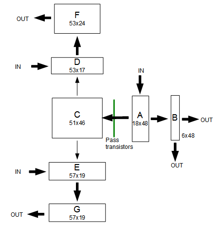
The following diagram shows the location of the ALU in the 8085. The ALU is 8 bits wide, with the high-order bit on the left. The register file is the large block below the ALU. The registers are 16 bits wide, made up of pairs of 8-bit registers. Surprisingly, the register file has the high-order bit on the right, the opposite order from the ALU.

The 8085 microprocessor, showing the location of the 8-bit ALU.

The ALU takes two 8-bit inputs, which I'll call A and X, and performs one of five basic operations: ADD, OR, XOR, AND, and SHIFT-RIGHT. As well, if the input X is inverted, the ALU can perform subtraction and complement operations. You might think SHIFT-LEFT is missing from this list. However, it is simply performed by adding the number to itself, which shifts it to the left one bit in binary. Note that the 8085 arithmetic operations are very basic. There is no multiplication or division operation - these were added in the 8086.

The ALU consists of 8 mostly-identical slices, one for each bit. For addition, each slice of the ALU adds the appropriate input bits, computing the sum A + X + carry-in, generating a sum bit and a carry-out bit. That is, each bit of the ALU implements a full adder. The logic operations simply operate on the two input bits: A AND X, A OR X, A XOR X. Shift-right simply outputs the A bit from the slice to the right.

ALU schematic

The following schematic shows one bit of the ALU. The schematic has roughly the same layout as the implementation on the chip, flowing from bottom to top. Eight of these circuits are stacked side-by-side, with the low-order bit on the right. Carries flow from right to left, and bits shifted right flow from left to right.

Schematic of one bit of the ALU in the 8085 microprocessor.

Negation

Starting at the bottom of the schematic, is the complex gate labeled Negation. This gate optionally selects a negated second argument by selecting either XN or /XN. (XN is the Nth bit of the second argument, which I'll call X. The / indicates the complement.) For most of the discussion below I'll assume XN is uncomplemented to keep things simpler.

Operation

Above the complement selector are a few gates labeled Operation that perform the desired 2-input operation. The NAND gate on the left generates either A NAND X or 1 based on the select_op1 control line. The OR gate on the right generates either A OR X or 1, based on the select_op2 control line. Combining these in the NAND gate yields four different possibilities:
select_op1select_op2Result
00A NOR X
010
10A NXOR X
11A AND X
Note that instead of OR and XOR, the complemented value is produced by this circuit. This will be fixed in the next step.

Combine with carry

Above the operation circuit is the next block of gates labeled Combine with carry that generates the ALU output by merging the carry-in with the operation value via XOR.

To understand this circuit, first consider the following simple XOR circuit, which is used a couple times in the ALU. It can be understood fairly simply: if both inputs are 0 (top) or both inputs are 1 (bottom) then the output is 0.

An XOR gate can be implemented by a NOR gate and an AND-NOR gate. This circuit is used in the 8085 ALU.

Ignoring the shift_right circuit for a moment, the block of gates is simply the XOR circuit above. Note that XOR with 0 is a no-op, while XOR with 1 complements the value. And A XOR X XOR CARRY is the low-order bit of adding A, X, and CARRY.

The key point of this circuit is that the incoming carry is generated with the proper value to convert the operation output into the desired final result. The incoming carry /carry(N-1) is either 0, 1, or the complemented carry from bit N-1 as appropriate.

OpOperation outputCarryResult
orA NOR X1A OR X
addA NXOR X/carryA XOR X XOR CARRY
xorA NXOR X1A XOR X
andA AND X0A AND X
shift right00A(N+1)
complementA NOR /X1A OR /X
subtractA NXOR /X/carryA XOR /X XOR CARRY

Note that the carry-in line must have the right value in order to generate the appropriate output. For addition it passes the inverted carry from one bit to the next. But for OR, XOR, the line is set to 1. And for AND and SHIFT_RIGHT it is set to 0. As will be seen below, the carry circuitry generates the right value for the right operation.

The final aspect of this circuit is the shift-right circuit. With a 0 op input, 0 carry input, and shift_right set, the output is simply the bit from the right: A(N+1).

Generate carry

The circuit on the left, labeled Generate carry generates the carry out. It can generate three different outputs: 1, 0, or the (complemented) carry from the sum. If select_op2 is set, it will force the carry to 0. Otherwise if force_ncarry_1 is set, it will force the carry to 1. Otherwise, the carry is generated for the sum of A + X + carry-in through straightforward logic: If the carry-in is set, and one of the inputs is set, there will be a carry out. If both input bits are set, there will be a carry out.

Flags

The 8085 has a parity flag, which is 1 if the number of 1 bits is even, and 0 if the number of parity bits is odd. The parity flag is generated by XORing all the result bits together (and complementing). Each bit is XORed with the lower-order parity value by the parity circuit near the top of the schematic. The XOR circuit is the same circuit described above.

The zero flag is computed by a simple circuit: each result bit drives a transistor that will pull the zero line low if the bit is set. This forms an 8-input NOR gate, spread across the ALU.

The control lines

As seen in the schematic, the 8085 uses multiple control lines to control the activity inside the ALU. In total, the ALU provides 7 different operations and the following table summarizes the control lines that are used for each operation. It also lists the opcodes that use each ALU operation.

Operationselect_negselect_op1select_op2shift_rightforce_ncarry_1Opcodes
or00001ORA,ORI (and default)
add01000INR,DCR,RLC,DAD,RAL,DAA,ADD,ADC,ADI,ACI (and undocumented LDSI,LDHI,RDEL)
xor01001XRA,XRI
and01101ANA,ANI
shift right00111RRC,RAR (ARHL)
complement10001CMA
subtract11000SUB,SBB,SUI,SBI,CMP,CPI (DSUB)

The ALU control lines are generated from the opcode by the programmable logic array. Specifically, they are outputs from PLA F, which is to the right of the ALU. More details are in my article on the PLA. The ALU has additional control lines to set up the registers, initialize the carry bits, and set the flags. These control the differences between different op codes, beyond the categories above. the I will explain those in a future article.

The PLA in the 8085

Reverse-engineering the ALU

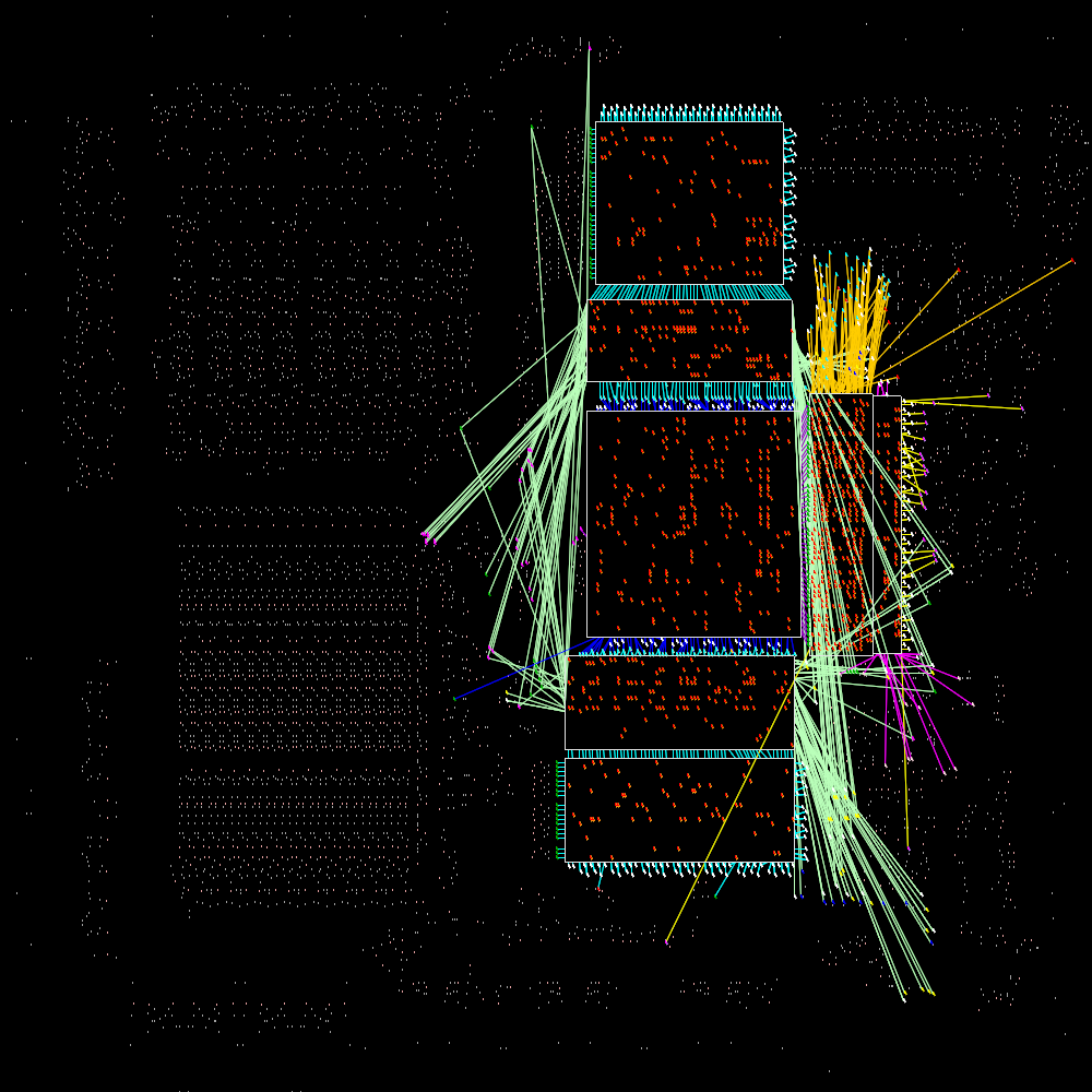
This information is based on the 8085 reverse-engineering done by the visual 6502 team. This team dissolves chips in acid to remove the packaging and then takes many close-up photographs of the die inside. Pavel Zima converted these photographs into mask layer images, generated a transistor net from the layers, and wrote a transistor-level 8085 simulator.

I took the transistor net and used it to figure out how the ALU works. First, I converted the transistor net into gates. Next I figured out which gates are part of the ALU and put them into a schematic. Then I examined how the circuit worked for different operations and eventually figured out how it works.

Conclusion

The ALU of the 8085 is an interesting circuit. At first it seemed like an incomprehensible pile of gates with mysterious control lines, but after some investigation I figured it out. The 8085 ALU is implemented very differently from the 6502's ALU (which I'll write up later). The 6502's ALU uses fairly straightforward circuits to generate the SUM, AND, XOR, OR, and SHIFT values in parallel, and then uses a simple pass-transistor multiplexor to pick the desired operation. This is in contrast to the 8085 ALU, which generates only the desired value.

Notes on the PLA on the 8085 chip

The 8085 processor uses a PLA (programmable logic array) to control much of the activity within the processor, such as instruction decoding and controlling the data flow between components of the chip. Pavel Zima has reverse-engineered the transistor-level circuitry of the 8085 microprocessor. I've looked into this in a bit more to figure out the architecture of the Programmable Logic Array, which takes up a large fraction of the chip. The PLA circuit is much more complex than the PLA on the 6502, for instance. It turns out that Pavel is ahead of me with information on the decode and timing PLAs, but the information below may still be of interest.

The following diagram shows the arrangement of the PLA on the chip (image from Visual 6502). The PLA has 5 planes, which I have labeled A through G.

The block diagram below shows approximately how the planes are connected. Plane A receives inputs from the instruction circuit. Its outputs are fed into the small plane B, producing outputs that go into the instruction circuit. The outputs from A also are fed into C (through pass transistors).

Planes D and E can be considered the same plane, split apart for better layout. They share 11 input lines, and the remaining inputs are different between D and E. These inputs come from the ALU/register circuits on the left, as well as other parts of the chip. They also receive inputs from G - these inputs are not handled via normal PLA input lines, but are wired through transistors directly to the associated output lines, which makes the layout more compact.

Planes F and G provide outputs through pass transistors to the ALU/register circuits. These outputs probably control the actions and bus activity, but more analysis is needed.

The following diagram shows how the PLA planes are wired to the rest of the chip. Planes D and E in particular receive inputs from many parts of the chip. The outputs from F and G are very short because the displayed wires end at the nearby pass transistors to the left.

The transistors in the PLA

I have diagrams showing where the transistors are in each PLA grid here.

The 6502 CPU's overflow flag explained at the silicon level

In this article, I show how overflow is computed in the 6502 microprocessor at the transistor and silicon level. I've discussed the mathematics of the 6502 overflow flag earlier and thought it would be interesting to look at the actual chip-level implementation. Even though the overflow flag is a slightly obscure feature, its circuit is simple enough that it can be explained at the silicon level.

The 6502 microprocessor chip

The 6502 is an 8-bit microprocessor that was very popular in the 1970s and 1980s, powering popular home computers such as the Apple II, Commodore PET, and Atari 400/800. The following photograph shows the die of a 6502 processor. Looking at the photograph, it seems impossibly complex, but it turns out that it actually can be understood, using the Visual 6502 group's reverse engineered 6502. The red box shows that part of the chip that will be explained in this article. The 6502 chip is made up of 4528 transistors (3510 enhancement transistors and 1018 depletion pullup transistors). (By comparison, a modern Xeon processor has over 2.5 billion transistors, which would be almost hopeless to try to understand.)

Photomicrograph of the 6502. The following diagrams zoom in on the red box, where the overflow circuit is located.

Photomicrograph of the 6502, from Visual 6502 (CC BY-NC-SA 3.0). The following diagrams zoom in on the red box, where the overflow circuit is located.

As a rough overview of the above photograph, the edge of the die shows the wires going to the pins. Approximately top fifth of the chip (with the regular rectangular pattern) is the PLA that decodes instructions. The middle third is a bunch of logic, mostly to do additional decoding of instructions. The bottom half has the registers, ALU (arithmetic-logic unit), and main busses. They are all 8 bits, with each bit in a horizontal layer. The high-order bit is at the bottom of the photo, and this is where the overflow logic lies.

The overflow formula

In brief, if an unsigned addition doesn't fit in a byte, the carry flag is set. But if a signed addition doesn't fit in a byte, the overflow flag is set. The 6502 processor computes the overflow bit for addition from the top bits of the two operands (A7 and B7), and the carry out of bit 6 into bit 7 (C6):

V = not (((A7 NOR B7) and C6) NOR ((A7 NAND B7) NOR C6))

For a more detailed explanation of what overflow means, see my previous article or The overflow flag explained.

Gate-level implementation

The overflow computation circuit in the 6502 microprocessor.

Described as gates, the actual circuit to generate the overflow flag in the 6502 turns out to be surprisingly simple. It uses the carry out of bit 6, and the top bits of the two arguments A and B. Since the values of NAND(a7, b7) and NOR(a7, b7) are already available in the ALU (Arithmetic-Logic Unit) for other purposes, the actual overflow circuit is simply the three gates on the right. (The ALU is, of course, much more complex than the part shown above.) This circuit can be seen at the bottom of the 6507 schematic (where the inverted overflow value is called FLOW). You might wonder why the circuit uses NAND and NOR gates so heavily; it turns out that these are much easier to implement with transistors than AND and OR gates.

Transistor-level implementation

The transistors that implement the overflow circuit in the 6502 microprocessor. The circuits on the left compute the NAND and NOR of the top bits of A and B. The circuit on the right computes the overflow flag.
The transistors that implement the overflow circuit in the 6502 microprocessor. The circuits on the left compute the NAND and NOR of the top bits of A and B. The circuit on the right computes the overflow flag. Based on the remarkable transistor-level schematic of the full 6502 chip, reverse-engineered by Balazs.

The circuit above shows the actual implementation of the overflow circuit in the 6502 using NMOS transistors. The circuit to generate the overflow flag is very simple, requiring just a few transistors to implement the three gates. A, B, and carry are the inputs, and the output #overflow indicates complement of the overflow signal.

MOS transistors are fairly easy to understand, since they operate like switches. Most of the transistors are NMOS enhancement mode transistors, which can be considered as switches that close if the gate has a positive input, and are open otherwise. The transistors with a black bar are NMOS depletion mode transistors, which can be considered as pull-up resistors, giving a positive output if nothing else pulls the output low.

The three transistors on the left implement a simple logic gate to compute NAND of A and B. If both inputs A and B are positive, the switches close and connect the output to ground (the horizontal line at the bottom). Otherwise, the pullup transistor connects the output to the positive voltage (circle at the top). Thus, the output is the NAND of A and B - 0 if both inputs are positive, and 1 otherwise.

The next three transistors compute NOR of A and B. If A, B, or both are positive, the associated transistor is switched on and connects the output to ground. Otherwise the output is positive.

The remaining transistors are the actual overflow circuit. The next group of three transistors is a NOR gate, which was described above. It computes the NOR of the carry and the NAND output from the ALU, feeding its output into the final group of four transistors. The four transistors on the right implement an AND gate and NOR gate in a single circuit. If the output from the previous circuit is 1, the rightmost transistor switches on, pulling the output (inverted V) to ground. If both NOR7 and CARRY6 are 1, the two associated transistors switch on, pulling the output to ground. Otherwise, the pullup transistor keeps the output high. The result is the complemented overflow value.

Going to the silicon

Now that you've seen how the circuit works at the transistor level, the silicon level can be explained.

We'll begin with an (oversimplified) description of how the chip is constructed. The chip starts with the silicon wafer. Regions are diffused with an element such as boron, yielding conductive n+ diffusion regions. On top of the polysilicon layer is a layer of metal "wires" providing more connections. For our purposes, diffusion regions, polysilicon, and metal can all be consider conductors. In the 6502, the polysilicon connections run roughly vertical, and the metal wires run generally horizontal.

Structure of an NMOS transistor

Structure of an NMOS transistor. The n+ diffusion regions (yellow) separated by undiffused silicon (gray). The gate is formed by an insulating oxide layer (red) with a diffusion line (purple) over it.

To build a transistor, two n+ regions are separated by an undiffused region. A thin insulating oxide layer on top forms the transistor gate, which is wired to a diffusion line. When charge is applied to the gate via the polysilicon line, the two n+ regions can conduct.

The follow picture zooms in on the base silicon layer in the 6502, showing the region in the red outline. The darker gray regions are n+ diffusion areas, which have been doped to be conducting. The white stripes that separate n+ regions are the transistor gates, showing the thin insulating oxide layer that switches on and off conduction between the neighboring n+ regions. The gray squares are vias, which connect to other layers.

The diffusion layer of the 6502, zoomed in on the overflow circuit. The white strips show transistor gates.

The diffusion layer of the 6502, zoomed in on the overflow circuit. The shaded regions are diffusion regions, and the unshaded regions are undiffused silicon. The white strips show transistor gates. From Visual 6502 (CC BY-NC-SA 3.0).

The next picture shows the polysilicon and metal layers that lie on top of the base silicon. This picture is aligned with the previous one, and you may be able to pick out some of the diffusion layer underneath. The whitish vertical stripes are conductive polysilicon. The greenish metallic-looking horizontal stripes are in fact metal, forming conductors. The gray square are vias, which connect different layers. Note that the chip is crammed full of conductors, making it hard at first glance to tell what is going on.

Closeup of the 6502 microprocessor die, showing the overflow circuit.

Closeup of the 6502 microprocessor die, showing the overflow circuit. From Visual 6502 (CC BY-NC-SA 3.0).
The following picture shows approximately how the transistor-level circuit maps onto the silicon. This circuit is the same as the transistor schematic earlier, just drawn to match the actual layout on the chip. The A, B, and CARRY inputs come from other parts of the chip, and the inverted #OVERFLOW output exits on the right to other destinations.

The 6502 overflow circuit at the transistor level, overlaid on the photomicrograph of the die.

The final picture explains exactly what is happening at the silicon level. It labels the different layers that take part in the overflow circuit with different colors. The lowest layer is the diffusion layer in yellow. On top of this is the polysilicon layer in purple. The topmost layer of metal is in green. Power (Vcc) and ground are supplied through the metal layer. The crosshatches show transistor gates, formed by polysilicon over insulating oxide. The skinny crosshatched areas are the enhancement transistors used as switches. The blocky crosshatched areas connected to Vcc (positive voltage) are the depletion transistors used as pullups.

The overflow circuit in the 6502 at the silicon level. The diffusion layer is yellow. Polysilicon is in purple. Metal is in green. Crosshatches show transistors.

The circuit can be understood starting in the upper left. A and B are bit 7 of the A and B values going into the ALU. (A and B come from elsewhere in the processor.) If A and B are positive, the two upper transistors (vertical crosshatches) will pull the NAND output low. If A or B are positive, one of the two transistors below will pull the NOR output low. The NAND and NOR outputs travel to multiple parts of the ALU through metal, polysilicon, and diffusion "wires", but only the relevant connections are shown.

In the lower left is the first gate of the overflow circuit, computing the NOR of the NAND output and carry (which comes from elsewhere in the chip). The polysilicon line (purple) on the bottom is the output from this gate. In the lower right is the second gate of the overflow circuit, combining the NOR, carry, and output of the first gate. The result is #overflow (i.e. inverted overflow).

You can see this circuit in action in the Visual 6502 simulator. The color scheme in the simulator is different - diffusion is green, yellow, orange, and red. The metal layer is shown in ghosted white, but Vcc and ground are omitted. Polysilicon is in purple, and the transistors are not explicitly shown.

Conclusions

By focusing on a simple circuit, the 6502 microprocessor chip can actually be understood at the silicon level. It's interesting to see how the complex patterns etched on the chip can be mapped onto gates, and their function understood.
More comments on this article are at Hacker News. Thanks for visiting!