This article reverse-engineers the flag circuits in the ARM1 processor, explaining in detail how the flags are generate, controlled, and used. Condition flags are a key part of most computers, since they allow the computer to change what it does based on various conditions. The flags keep track of conditions such as a value being negative or zero or an overflow happening. Processors may also have status flags to control modes such as running in user mode versus protected (kernel) execution. The ARM1 processor stores these flags in a special register called the Processor Status Register (PSR).[1]
The ARM1 chip is interesting to examine not only because it is simple enough to understand but also because it was the first ARM processor. There are now tens of billions of ARM processors in use, probably powering your smartphone right now. This article is part of my series on reverse-engineering the ARM1. Processor flags seem like they should be trivial, but there's a lot more involved than you might expect. You might want to start with my first article for an overview of the chip.
The die photo below shows the ARM1 chip. This article concentrates on the flag logic, highlighted in red. As you can see, flags take up a significant part of the chip. The flags interact with many other parts of the chip: the trap control logic handles interrupts and exceptions; the register control logic handles access to the chip's registers including the program counter (PC); when the Arithmetic-Logic Unit (ALU) performs computations it stores status in the flags; the Barrel Shifter shifts or rotates values, sending shifted bits to the flags; and the Instruction Register holds instructions as they are read from memory and feeds them to the decode logic to be interpreted. In the upper left, the M0 and M1 pins indicate the mode bits stored in the flags. The article will describe how all these components interact with the flags.

Some ARM1 background
This section summarizes a few features of the ARM1 processor that are important for understanding the flags. The ARM1 is a 32-bit processor with 16 32-bit registers called R0 through R15 (and some extra registers that will be described later). The processor has a 26-bit address space.One unusual feature of the ARM1 processor is it combines the flag bits in the processor status register (PSR) and the program counter (PC) into a single register, R15, the PC/PSR. Because of the 26-bit address space, the top 6 bits of the 32-bit PC register are unused. In addition, instructions are always aligned on a 32-bit boundary, so the bottom two PC bits are always 0. These eight unused PC bits were instead used for flags, as shown in the diagram below.[2]

Four condition flags hold the status of arithmetic operations or comparisons. The negative (N) flag indicates a negative result. The zero (Z) flag indicates a zero result. The carry (C) flag indicates a carry from an unsigned value that doesn't fit in 32 bits. The overflow (V) flag indicates an overflow from a signed value that doesn't fit in 32 bits. The next two bits are used to enable or disable interrupts: the I flag controls regular interrupts, while the F flag controls the chip's special fast interrupts. The bottom two bits (M1 and M0) control the processor's execution mode: user, supervisor (kernel), interrupt handler, or fast interrupt handler. These modes will be discussed in more detail later.
Two instruction classes that are important to flags are the data processing instructions and the block data transfer instructions. Since the ARM has a simple, orthogonal instruction set, these operations can operate on the R15 with the flags as easily as any of the other registers.
The data processing instructions are the arithmetic-logic instructions. There are 16 types of data processing operations, such as addition, subtraction, Boolean operations such as AND, and comparison. Unlike most processors, the ARM makes updates of the condition flags optional. The instruction includes a bit called the "S" bit. If the S bit is set, the instruction updates the condition flags; otherwise the flags remain unchanged. The data processing instructions can also act on R15 directly, causing the flags to be read or modified.
The ARM also provides block data transfer instructions: LDM (load multiple) and STM (store multiple). These instructions load a selected set of registers from memory or store them to memory, for example popping registers from the stack or pushing them to the stack. These instructions can also use R15, accessing or modifying the flags.
")
While the program counter (PC) and flags are architecturally part of the same register R15, they are physically separated on the chip, as you can see from the die photo and the floorplan diagram above. The flags are labeled PSR, above the ALU, while the PC is on the left of the register file. Interestingly, the original sketch for the ARM1 (below) show the PSR flags right next to the PC. While the final chip architecture largely matched the sketch, some components moved. In particular, several functional units were moved to the top of the chip, above the instruction bus (orange).
 is on the left; the final chip put it above the ALU. Photo courtesy of Ed Spittles.")
The flag circuitry
The diagram below shows the flag circuit of the chip as it appears in the simulator; this is a zoomed-in version of the red rectangle indicated on the die earlier.The chip consists of multiple layers, indicated by different colors below. Transistors appear as red or blue regions. NMOS transistors are red; they turn on with a 1 input and can pull their output low. PMOS transistors (blue) are complementary; they turn on with a 0 input and can pull their output high. Physically above the transistors is the polysilicon wiring layer (green). When polysilicon crosses a transistor it forms the gate (yellow) that controls the transistor. Finally, two layers of metal wiring (gray) are above the polysilicon.

The flag circuit above has been partitioned into several components. At the bottom are the circuits to store the eight flags. In the upper left, the flag control circuitry generates signals that control flag use and updates. The mode control circuit in the upper right generates the signals to update the mode bits M0 and M1. Finally, the register control circuit uses the mode bits to select a register bank. At the bottom is the wiring that connects the B bus, ALU bus, and flag inputs to the flag circuits.
The remainder of this article will start by discussing a single flag, the N flag at the bottom. Next it will describe the condition flags (V, C, Z and N) in more detail, along with how the flag control circuit (schematic) creates the control signals. This will be followed by an explanation of the mode flags (M0, M1) and the interrupt flags (F, I) and their control signals. The article ends with a discussion of the register bank select circuit.
The circuit to store a flag
This section discusses how the negative (N) flag works. The other flags operate similarly, but with some differences, and will be discussed in later section. The schematic below shows the circuit for the negative flag; this flag is at the bottom of the chip layout above. If you're expecting flags to be stored in a flip flop or regular latch, this circuit may seem unusual. Flags are stored in a dynamic two-phase flip-flop, which uses stray capacitance to store the value. The basic idea is the value goes around in a loop, amplified by the four inverters, and controlled by the clock. The trapezoids in the schematic are pass-transistor multiplexers[3] Each multiplexer has two inputs and two control lines; if a control line is active, the corresponding input is connected to the output.
 in the ARM1. The flag is stored in a two-phase dynamic latch. Two multiplexers (trapezoids) select values to store in the flag.")
The storage loop consists of two parts, alternately connected by the clock. During the first clock phase, Φ1, the multiplexer on the left is inactivated by its inputs and generates no output. It holds its previous output due to stray capacitance at the point marked "hold during Φ1". The signal goes around the loop, through the Φ1 transistor on the right, and up to the input of the multiplexer. When the clock switches to Φ2, the multiplexer becomes active again, and the transistor on the right switches off. Now, the signal to the left of the transistor is held by the capacitance and flows around the loop until it reaches the transistor and is blocked. Thus, during each clock phase, half the loop is stable and half the loop can be updated. Alternatively, you can consider each half a simple latch and the two parts form a master-slave latch.
The main use of the condition flags is for conditional instructions — executing an instruction if the condition is satisfied. The flag out wire in the diagram goes to the conditional instruction logic which controls execution by checking the flag values to determine if the condition is satisfied (details),
The typical way the condition flags are updated is after performing a data processing operation, e.g. ADD. If the result is negative, the N flag is set; otherwise, the N flag is cleared. The multiplexer on the right allows the new flag value from the ALU to be selected instead of the recirculating value. This happens if the aluflag control signal is activated.
The second way to update the condition flags is to write to them directly, for instance to restore the flag values after handling an interrupt. The flags can be written from the ALU data bus (which is different from the flag value from the ALU described earlier). The multiplexer on the left selects this value instead of the recirculating value if the writeflags signal is active.
The condition flags can be read directly, for instance to save the flag values while handling an interrupt. The transistors on the left allow the flags to be written to the B bus when the psr_oen (PSR output enable) control signal is activated.
The diagram below zooms in on the chip layout of the N flag, which can be compared with the schematic. The wire that recirculates the flag from the right to the left is indicated. You can see the transistors that form the inverters and multiplexers. Details on how the red NMOS transistors and blue PMOS transistors work together to form inverters are here.
 in the ARM1 processor.")
The conditions flags in detail
The flags all roughly follow the circuit described above, but there are differences since the flags have different behaviors. The schematic below shows the circuits for the four condition flags: V, C, Z and N. This section describes these flags in detail, along with how the control signals are generated. By comparing the chip logic with the documentation, we can see how the described behavior is implemented in the logic.Generating the flags
Each flag is generated in a different way. The N (negative) flag is very simple. A signed number is negative if the top bit is set, so the N flag is simply loaded from the top bit of the ALU bus.The Z (zero) flag is generated by the ALU. The ALU in effect does a NOR of all 32 output bits; if all bits are zero, the Z flag is 1. For efficiency, the ALU uses a chain of alternating NAND and NOR gates, but the effect is the same.
Generating the C (carry) flag is quite complicated. For arithmetic operations, the carry flag is the carry out from bit 31 of the ALU: this is the carry for addition and not-borrow for subtraction. The ARM1 supports a variety of shift operations, which affect the carry in different ways, so logic gates select different bits from the shifter depending on the instruction. It may be the bit shifted out on the left, the bit shifted out on the right, the carry flag, the left bit or the right bit.
The V (overflow) flag indicates overflow of a signed value. If two signed values are added or subtracted, the result may not fit in 32 bits, and this is indicated by setting the overflow flag. An overflow occurs if the carry out from bit 30 being different from the carry out from bit 31 and is computed by XOR of these two bits. I discuss signed overflow in detail here.

Updating the condition flags with results of an operation
One feature that distinguishes the ARM processor from most other processors is that condition flag updates are optional. If an arithmetic operation has the S bit (bit 20) set, the flags are updated, otherwise they are not. By looking at how the aluflag control signal is generated, we can see how this functionality is implemented.
")
If the aluflag control signal[4] is high, the multiplexer on the right will select the flag value generated by the ALU, rather than the recirculated value. The aluflag control signal is activated if pla1_aluproc from the instruction decoder is set (details) and if the S bit (bit 20) is set in the instruction register. The pla1_aluproc line is set when the ALU is doing a data processing operation, but not when the ALU is, for example, computing an address offset. This is why the condition flags are updated only for relevant operations. If an abort of the instruction occurs, aluflag is blocked, preventing the flags from being modified.
Arithmetic versus logic operations
The following text from the ARM databook explains the behavior of the condition flags during a data processing (ALU) operation. The part of interest is that the carry (C) and overflow (V) flags are treated differently for logical operations versus arithmetic operations.

The schematic shows the circuits that explain this behavior. The control line pla1_aluarith is generated by the instruction decode logic (details); it is high if the ALU operation is an arithmetic operation (e.g. ADD), and low for a logic operation (e.g. AND). This control line selects the different C and V inputs for arithmetic or logical operations. For the C flag, this control line selects between the ALU's carry out and the shifter's carry out. (The shifter has a lot of logic because the carry out depends on the type and direction of shifting.) For the V flag, this control line selects between the ALU's overflow signal and the old V flag — this is why logic operations don't update the V flag.
Writing the flags directly
As described earlier, the flags and the Program Counter share register R15, so storing a value in R15 can update the flags. This is implemented through the multiplexer on the left. If control signal writeflags is activated, the multiplexer on the left will select the value from the ALU bus, rather than the recirculated value, updating the flags with the new value. Otherwise, nowriteflags is activated, selecting the recirculated value and leaving the flag unchanged. (Note that both writeflags and nowriteflags are inactive during clock phase Φ1, effectively disconnecting the multiplexer output.)The generation of writeflags is relatively complicated. First, if pla_psrw this indicates a block copy instruction (LDM/STM) is writing to the PSR; if instruction register bit 22 (S) is set the flags will be updated. Second, aluflag (described above) indicates an ALU data processing operation should update the flags. In either of these cases, as long as abort is clear, and wpc (write PC) is set, then the nowriteflags1 signal is active. This signal is combined with the clock Φ2 to generate the writeflags and opposite nowriteflags signals sent to the multiplexer. This implements the logic described on page 2-34 for data processing instructions:

Reading the flags
Looking at the block diagram of the ARM1 process explains some of the behavior when reading the flags. A data processing instruction specifies three registers: the operation is performed on the first two registers and the result stored in the third. The first register (Rn) is read over the A bus. The second register (Rm) is read over the B bus and goes through the barrel shifter. The ALU generates the result of the operation, which is stored to a third register (Rd) via the ALU bus.

The block diagram above shows how the flags are connected to the chip's buses. The flags are separate from the register file; they are written via the ALU bus and read via the B bus. Thus, the flag value in R15 can only be accessed as the second register (Rm) via the B bus, and not as the first register (Rn) via the A bus. This explains the behavior described in the manual:

The process to write data to the B bus may seem backwards. The B bus is complemented, so a 1 on the bus indicates a 0 value. In more detail, the B bus is pulled high in clock phase Φ2 by transistors on the right of the register file (details). In clock phase Φ1, anyone writing to the bus sends a 1 by pulling the corresponding bus line low.[5] From the schematic, you can see that the control signal psr_oen (PSR output enable) controls putting the (complemented) flag values on the B bus. If psr_oen is active (only in phase Φ1) and the flag value is 1, the output transistors will pull the bus to 0.
The psr_oen signal is enabled to read the flags in two cases. The first happens when flags are being saved to R14 for a trap. The pla2_psren (PSR enable) signal controls this; it comes from instruction decoding at the start of a software interrupt (SWI), coprocessor instruction (i.e undefined instruction), or interrupt. The second case is when the R15 is being read via the B bus. This is indicated when pla2_ben (B Enable) and bpc (B bus PC) are active. The pla2_ben signal (PSR enable) comes from instruction decoding and is enabled at some point during most instructions. The register file generates the bpc signal when the B bus accesses the PC.
The mode and interrupt flags
This section discusses the M0 and M1 (processor mode) flags and the I and F (interrupt) flags. The behavior of these flags is different in several ways from the condition code flags, and their circuitry is significantly different.The four modes of the ARM1 are:
| M1 | M0 | Mode |
|---|---|---|
| 0 | 0 | User |
| 0 | 1 | Fast Interrupt (FIRQ) |
| 1 | 0 | Interrupt (IRQ) |
| 1 | 1 | Supervisor (SVC) |
When an exception trap occurs, the trap logic directs the flag circuitry to switch the mode. An interrupt switches to Interrupt mode, a fast interrupt switches to Fast Interrupt mode, and any other exception (reset, undefined instruction, memory abort, etc) switches to Supervisor mode. The trap logic indicates the new mode through the signals psrbank1 and psrbank0:
| Exception | psrbank1 | psrbank0 |
|---|---|---|
| Fast Interrupt | 0 | 1 |
| Interrupt | 1 | 0 |
| Reset | 1 | 1 |
| Other | 0 | 0 |
Note that the psrbank values don't exactly match the M0/M1 values. The psrbank values pass through a few gates in the mode control logic to generate newM1 and newM0 which are stored into the flags.
As the schematic shows, control signal oldstatus causes the flags to keep their old value, while newstatus loads the new value when a fault occurs. The newstatus signal is generated from instruction decode signal pla2_banken, which is activated during a SWI (software interrupt) instruction, coprocessor instruction (causing an undefined instruction fault), or an interrupt. It is blocked by the abort signal. Otherwise oldstatus is activated. Both signals can only be active during clock phase Φ1.

The other multiplexer signals are psr_t0, which loads the flags from the ALU bus, and psr_t1, which uses the value from the previous multiplexer. Both signals can be active only during clock phase Φ2, so the two multiplexers alternate. The psr_t0 signal is the same as writeflags used by the condition flags, except it is blocked if the mode flags indicate user mode. This is how the ARM1 prevents the mode and status flags from being updated in User mode (which is necessary for security). The psr_t1 signal is the opposite of psr_t0 (not exactly inverted since both are low during Φ1).
Moving on to the interrupt flags, any fault causes the I flag to be set (preventing an interrupt while the fault is being handled). This is accomplished by the 1 input to the I register multiplexer. The F flag is set (blocking fast interrupts) on reset and when a fast interrupt occurs. The schematic shows that F will be set if psrbank0 is high, and keeps its old value otherwise (via the OR gate). Since psrbank0 is high for fast interrupts and reset, the desired behavior is obtained.
One interesting thing about the M0 and M1 flags is they are connected directly to the M0 and M1 output pin driver circuits, shown below. This circuit supports tri-state output (electrically disconnecting the output so the signal can be controlled externally) as well as input, even though neither of these features is used for the M0 and M1 pins. The reason is the same pin driver circuit is reused for all the ARM1 output pins regardless of whether or not they need these features. This is another example of how the ARM1 was designed for simplicity, rather than optimizing the design. Note that large transistors to provide the output current to the pin.

Register control
One feature of the ARM1 processor is has multiple register banks, controlled by the mode flags. While there are 16 logical registers (R0 through R15), there are 25 physical registers. Each of the four modes has its own R13 and R14. The fast interrupt mode also has its own R10, R11 and R12.[6] These register banks improve performance by allowing interrupt handlers to use registers without needing to save the user registers.
The flag circuitry generates the signals that select the register bank. These signals go to the registers control circuitry next to the registers, where they are used to select particular registers
details).
The bank select signals are
bs0: general (non-fast-interrupt) registers.
bs1: fast interrupt registers.
bs2: regular interrupt registers.
bs3: supervisor registers.
bs4: user registers.
These (low-active) signals are generated from the M0 and M1 flags, which specify the mode. Registers R10-R12 use bs0 and bs1 to select the appropriate bank for fast interrupts or otherwise. Registers R13 and R14 use bs1, bs2, bs3 and bs4 to select between the four register banks.
One complication is for LDM/STM instruction, the S flag causes the user register bank to be used instead of the expected register bank. (This is a feature so interrupt handlers can access user registers if desired.) This happens if the pla2_psrw line is high, indicating a LDM/STM instruction; instruction register bit 22 is high (the S bit for LDM/STM); and pla2_nben is low, indicating bus B enabled. The pla2_psrw and pla2_nben signals are generated by the instruction decode circuits (details).
Conclusion
I expected to write a brief article on the ARM1 flags, but the topic turned out to be more complex than I expected. This article got a bit out of hand, so congratulations if you made it to the end! The flags are not the simple 8-bit register I expected, but are stored in dynamic latches with many control lines and inputs. With careful examination, it is possible to explain how the features and special cases described in the manual are implemented in the circuits. Studying the flags also explains the function of several of the control signals generated by the instruction decoder.Now that you've seen the internals of the flag logic, you can use the Visual ARM1 simulator to see the circuit in action. Thanks to the Visual 6502 team for providing the simulator and ARM1 chip layout data. For more articles on ARM1 internals, see my full set of ARM posts and Dave Mugridge's series of posts.
For my latest articles, follow me on Twitter here.
Notes and references
[1] Flags do not need to be bits in a register. The IBM 1401 and Intel 8008, for instance, do not have status flags as part of a register. Flags in these computers were not assigned bit positions but exist more abstractly. The Z-80 on the other hand, stores flags both in discrete latches and in a flag register, copying the flags between the two. The MIPS architecture doesn't have condition flags at all, but does both the test and the branch in the conditional branch instructions.[2] Was combining the flags and program counter into a single register in the ARM1 a clever idea or just bizarre? On the positive side, this allowed the flags and PC to be saved or restored in a single transfer, rather than two operations. It also allowed flags to be accessed without special flag instructions. On the negative side, restricting the address space to 26 bits was bad in the long term. This decision also prevented adding more flags in the future. Combining the flags and PC in register R15 also required special-case handling for R15 for many instructions.
The ARM architecture moved away from the combined PC/flags with the ARMv3 architecture. The flags were moved to separate registers: CPSR (Current processor status register) and SPSR (Saved Processor Status Register), allowing 32-bit addressing as well as additional flags and modes. New instructions (MSR, MRS) were added to access the CPSR and SPSR. (One ARMv3 processor of note is the ARM610, used in the Apple Newton.) Details on the historical and modern ARM status registers are here.
(The ARM numbering scheme is rather confusing. Architecture version numbers (e.g. ARMv3) don't match up with the CPU numbers (e.g. ARM6). More information on the ARM family numbering is here.)
[3] I discussed how the multiplexers in the ARM1 work earlier. In brief, each input has an NMOS and PMOS transistor working together as a switch, allowing the input to be connected to the output. The schematics show a single control line for each input; the implementation has two lines since the PMOS control signal must be inverted.
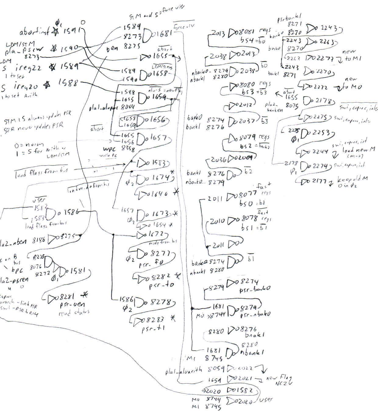
[4] Each signal in the simulator has a reference number that can be used to cross-reference the signals in other articles. Here are the key control signals used in the flags circuitry and their reference numbers:
| abort | 1591, 1655 |
| aluflag | 2021 |
| bpc | 8076 |
| bs0 | 8077 |
| bs1 | 8078 |
| bs2 | 8079 |
| bs3 | 8080 |
| bs4 | 8081 |
| instruction reg 22 | 8141 |
| instruction reg 20 | 8139 |
| newM0 | 2273 |
| newM1 | 2272 |
| newstatus | 2244 |
| nowriteflags | 1654 |
| nowriteflags1 | 1657 |
| oldstatus | 2177 |
| pla_psrw | 8273 |
| pla1_aluarith | 8059 |
| pla1_aluproc | 8064 |
| pla2_banken | 8075 |
| pla2_ben | 8275 |
| pla2_nben | 8186 |
| pla2_psren | 8272 |
| pla2_psrw | 8273 |
| psr_oen | 8281 |
| psr_t0 | 8282 |
| psr_t1 | 8283 |
| psrbank0 | 8270 |
| psrbank1 | 8271 |
| wpc | 8358 |
| writeflags | 1640 |
[5] You might wonder why the bus works in this way. This clocked dynamic logic is simpler than using logic gates to control the signal on the bus; only two transistors are needed to write a bit to the bus and they can be attached to the bus at any location. But why complement the bus? The reason is that it's easier with CMOS to pull a line low than to pull a line high. An NMOS transistor can provide more current than a similar PMOS transistor. And the reason for that is electrons (which carry the charge in NMOS) move faster than holes (which carry the charge in PMOS). Ultimately, the B bus is complemented due to semiconductor physics. (The Z-80 is another chip that has as complemented data bus.)
[6] Later versions of the ARM architecture introduced additional modes and more duplicated banks. Details are at ARMwiki.
3 comments:
An NMOS transistor can provide more current than a PMOS? Should that not be an NMOS transistor can provide current faster than a PMOS - electrons being more agile than holes?
I'd be interested to know what software you used? I used to use some from Cadence around the time this was made and ISTR the layout could be back translated into a cct net for something this size in around a day (including parasitics etc) and that could be used to check layout and cct matched.
Unknown: the current is due to the flow of electrons or holes, so faster-moving electrons result in lower impedance and more current with NMOS (for the same sized transistor).
For software, I'm using the Visual ARM1 simulator, as well as a bunch of scripts I've hacked together to convert the netlist into gates.
That's true for the same doping density and profile. Its around 36 years since I used to design these things and ISTR the obvious (electrons being faster than holes say) is not always the answer. The doping method can result in the silicon crystal structure being disturbed (increasing resistance) and doping N to same level of P may not be achievable.
There is (was) software that could convert a layout into gates (and parasitics)so in theory you should be able to dump the CIF file into it and get a gate level output - or indeed a full spice listing with parasitics if you can find out the silicon process details.
Tom
Post a Comment