The groundbreaking Intel 386 processor (1985) was the first 32-bit processor in the x86 line. It has numerous internal registers: general-purpose registers, index registers, segment selectors, and more specialized registers. In this blog post, I look at the silicon die of the 386 and explain how some of these registers are implemented at the transistor level. The registers that I examined are implemented as static RAM, with each bit stored in a common 8-transistor circuit, known as "8T". Studying this circuit shows the interesting layout techniques that Intel used to squeeze two storage cells together to minimize the space they require.
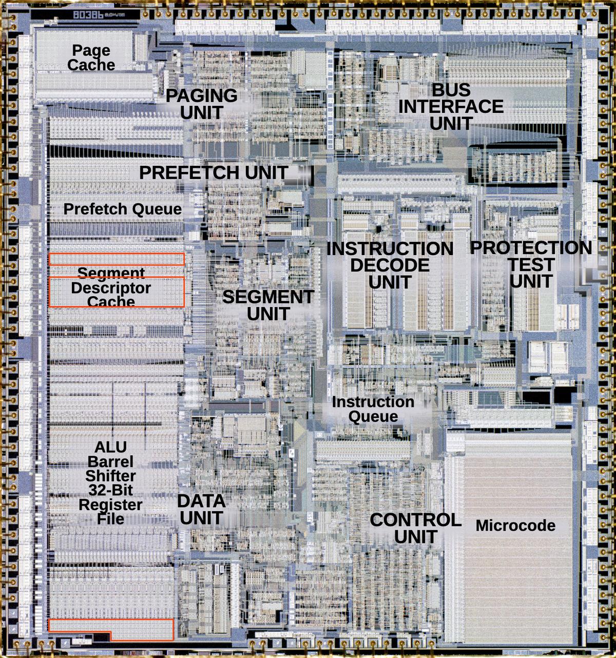
The diagram below shows the internal structure of the 386. I have marked the relevant registers with three red boxes. Two sets of registers are in the segment descriptor cache, presumably holding cache entries, and one set is at the bottom of the data path. Some of the registers at the bottom are 32 bits wide, while others are half as wide and hold 16 bits. (More registers with different circuits, but I won't discuss them in this post.)
The 6T and 8T static RAM cells
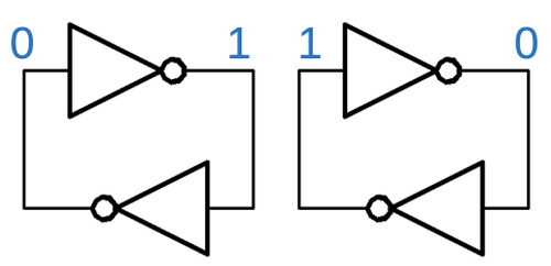
First, I'll explain how a 6T or 8T static cell holds a bit. The basic idea behind a static RAM cell is to connect two inverters into a loop. This circuit will be stable, with one inverter on and one inverter off, and each inverter supporting the other. Depending on which inverter is on, the circuit stores a 0 or a 1.
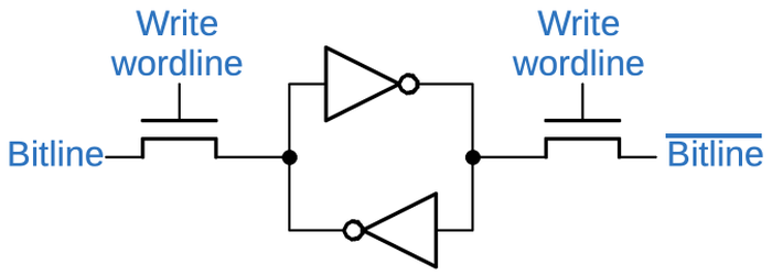
To write a new value into the circuit, two signals are fed in, forcing the inverters to the desired new values. One inverter receives the new bit value, while the other inverter receives the complemented bit value. This may seem like a brute-force way to update the bit, but it works. The trick is that the inverters in the cell are small and weak, while the input signals are higher current, able to overpower the inverters.1 The write data lines (called bitlines) are connected to the inverters by pass transistors.2 When the pass transistors are on, the signals on the write lines can pass through to the inverters. But when the pass transistors are off, the inverters are isolated from the write lines. Thus, the write control signal enables writing a new value to the inverters. (This signal is called a wordline since it controls access to a word of storage.) Since each inverter consists of two transistors7, the circuit below consists of six transistors, forming the 6T storage cell.
The 6T cell uses the same bitlines for reading and writing. Adding two transistors creates the 8T circuit, which has the advantage that you can read one register and write to another register at the same time. (I.e. the register file is two-ported.) In the 8T cell below, two additional transistors (G and H) are used for reading. Transistor G buffers the cell's value; it turns on if the inverter output is high, pulling the read output bitline low.3 Transistor H is a pass transistor that blocks this signal until a read is performed on this register; it is controlled by a read wordline.
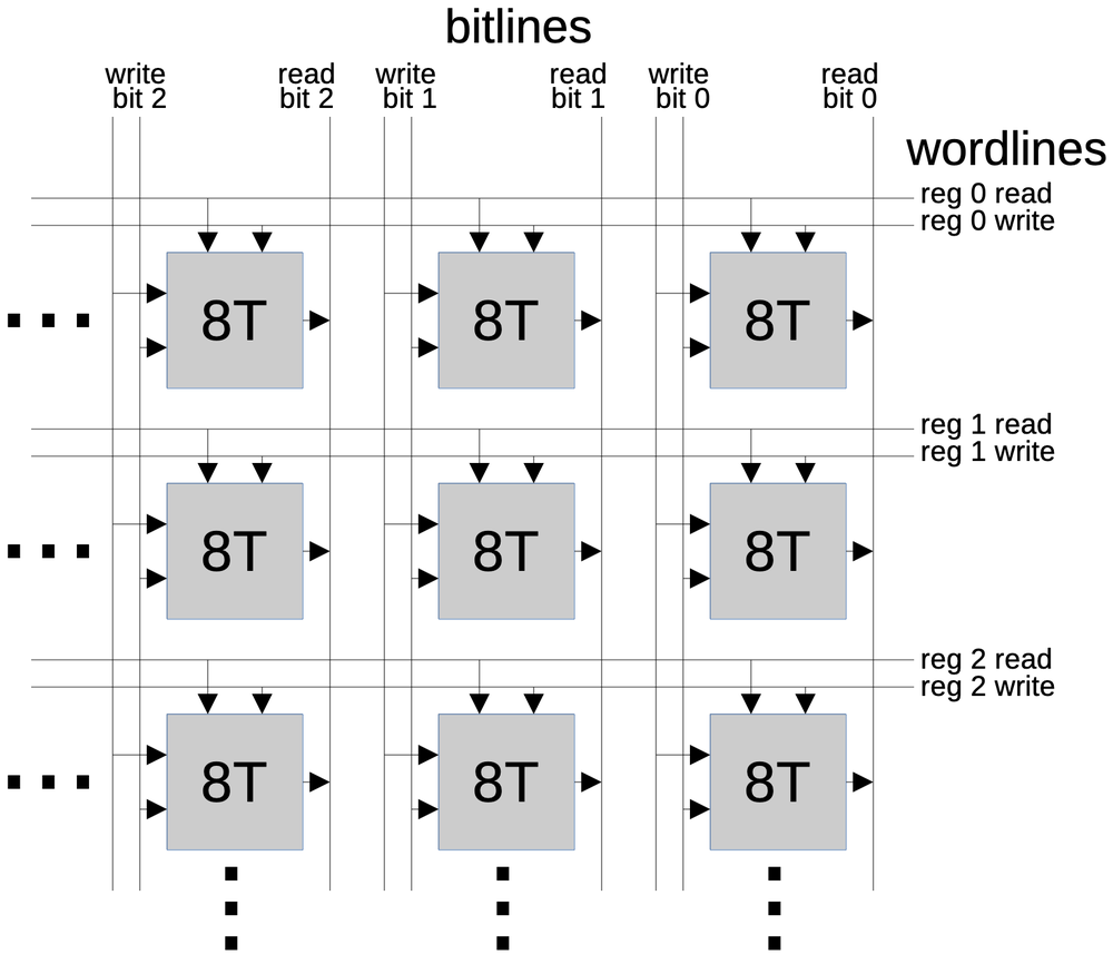
To form registers (or memory), a grid is constructed from these cells. Each row corresponds to a register, while each column corresponds to a bit position. The horizontal lines are the wordlines, selecting which word to access, while the vertical lines are the bitlines, passing bits in or out of the registers. For a write, the vertical bitlines provide the 32 bits (along with their complements). For a read, the vertical bitlines receive the 32 bits from the register. A wordline is activated to read or write the selected register.
Silicon circuits in the 386
Before showing the layout of the circuit on the die, I should give a bit of background on the technology used to construct the 386. The 386 was built with CMOS technology, with NMOS and PMOS transistors working together, an advance over the earlier x86 chips that were built with NMOS transistors. Intel called this CMOS technology CHMOS-III (complementary high-performance metal-oxide-silicon), with 1.5 µm features. While Intel's earlier chips had a single metal layer, CHMOS-III provided two metal layers, making signal routing much easier.
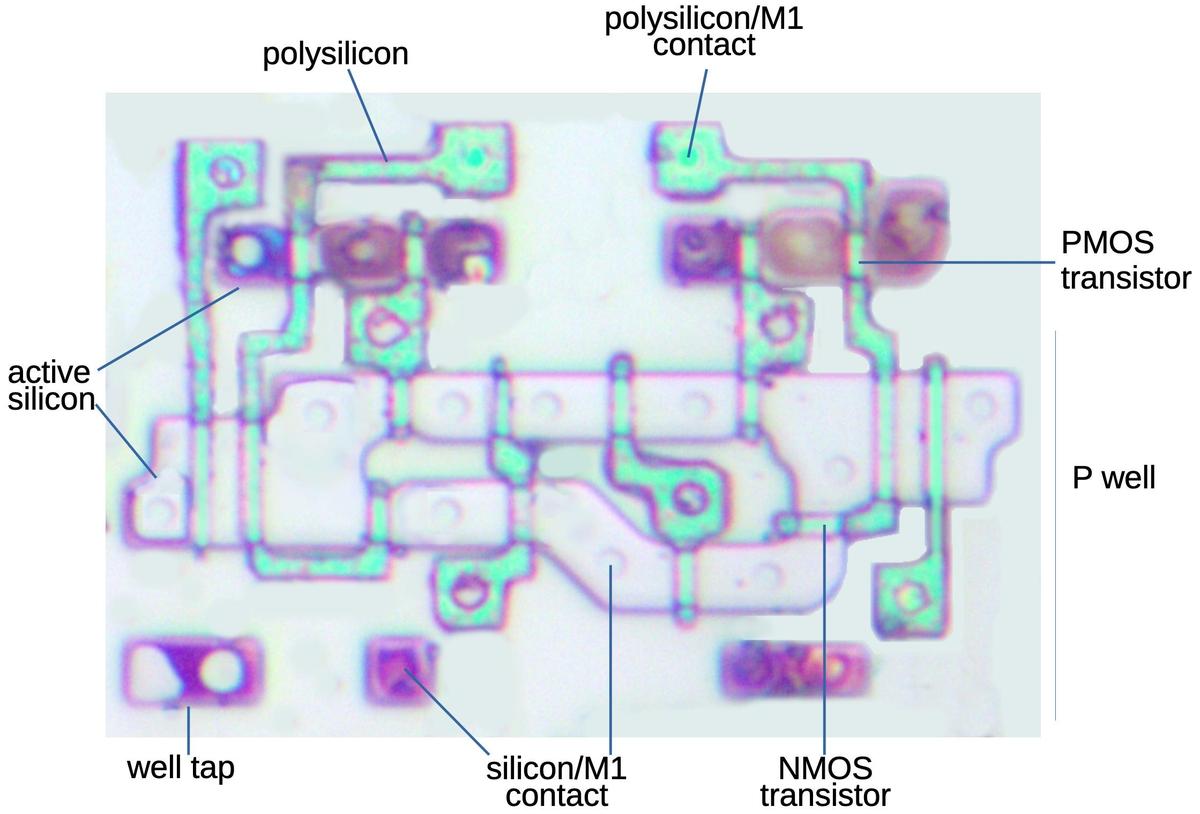
Because CMOS uses both NMOS and PMOS transistors, fabrication is more complicated. In an MOS integrated circuit, a transistor is formed where a polysilicon wire crosses active silicon, creating the transistor's gate. A PMOS transistor is constructed directly on the silicon substrate (which is N-doped). However, an NMOS transistor is the opposite, requiring a P-doped substrate. This is created by forming a P well, a region of P-doped silicon that holds NMOS transistors. Each P well must be connected to ground; this is accomplished by connecting ground to specially-doped regions of the P well, called "well taps"`.
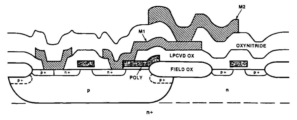
The diagram below shows a cross-section through two transistors, showing the layers of the chip. There are four important layers: silicon (which has some regions doped to form active silicon), polysilicon for wiring and transistors, and the two metal layers. At the bottom is the silicon, with P or N doping; note the P-well for the NMOS transistor on the left. Next is the polysilicon layer. At the top are the two layers of metal, named M1 and M2. Conceptually, the chip is constructed from flat layers, but the layers have a three-dimensional structure influenced by the layers below. The layers are separated by silicon dioxide ("ox") or silicon oxynitride4; the oxynitride under M2 caused me considerable difficulty.
The image below shows how circuitry appears on the die;5 I removed the metal layers to show the silicon and polysilicon that form transistors. (As will be described below, this image shows two static cells, holding two bits.) The pinkish and dark regions are active silicon, doped to take part in the circuits, while the "background" silicon can be ignored. The green lines are polysilicon lines on top of the silicon. Transistors are the most important feature here: a transistor gate is formed when polysilicon crosses active silicon, with the source and drain on either side. The upper part of the image has PMOS transistors, while the lower part of the image has the P well that holds NMOS transistors. (The well itself is not visible.) In total, the image shows four PMOS transistors and 12 NMOS transistors. At the bottom, the well taps connect the P well to ground. Although the metal has been removed, the contacts between the lower metal layer (M1) and the silicon or polysilicon are visible as faint circles.
Register layout in the 386
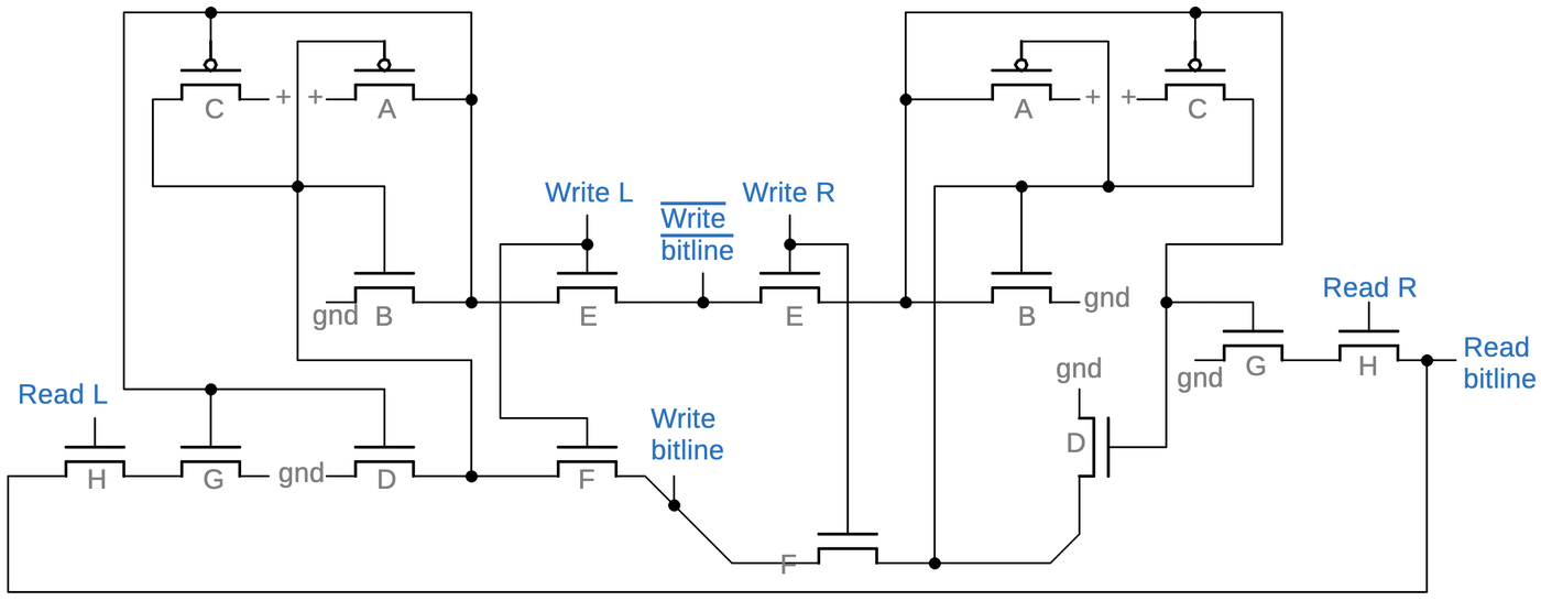
Next, I'll explain the layout of these cells in the 386. To increase the circuit density, two cells are put side-by-side, with a mirrored layout. In this way, each row holds two interleaved registers.6 The schematic below shows the arrangement of the paired cells, matching the die image above. Transistors A and B form the first inverter,7 while transistors C and D form the second inverter. Pass transistors E and F allow the bitlines to write the cell. For reading, transistor G amplifies the signal while pass transistor H connects the selected bit to the output.
The left and right sides are approximately mirror images, with separate read and write control lines for each half. Because the control lines for the left and right sides are in different positions, the two sides have some layout differences, in particular, the bulging loop on the right. Mirroring the cells increases the density since the bitlines can be shared by the cells.
The diagram below shows the various components on the die, labeled to match the schematic above. I've drawn the lower M1 metal wiring in blue, but omitted the M2 wiring (horizontal control lines, power, and ground). "Read crossover" indicates the connection from the read output on the left to the bitline on the right. Black circles indicate vias between M1 and M2, green circles indicate contacts between silicon and M1, and reddish circles indicate contacts between polysilicon and M1.
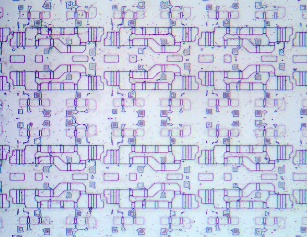
One more complication is that alternating registers (i.e. rows) are reflected vertically, as shown below. This allows one horizontal power line to feed two rows, and similarly for a horizontal ground line. This cuts the number of power/ground lines in half, making the layout more efficient.
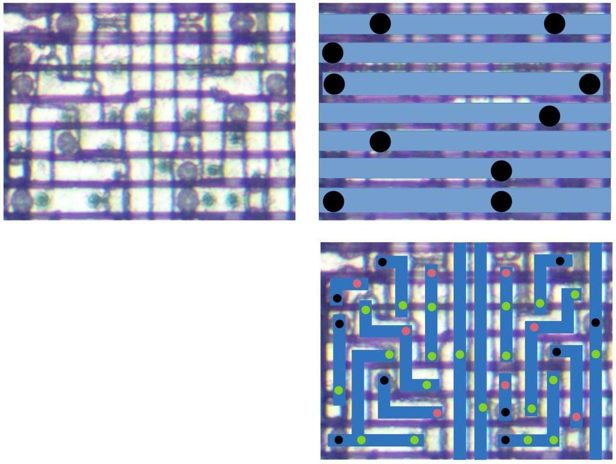
Having two layers of metal makes the circuitry considerably more difficult to reverse engineer. The photo below (left) shows one of the static RAM cells as it appears under the microscope. Although the structure of the metal layers is visible in the photograph, there is a lot of ambiguity. It is difficult to distinguish the two layers of metal. Moreover, the metal completely hides the polysilicon layer, not to mention the underlying silicon. The large black circles are vias between the two metal layers. The smaller faint circles are contacts between a metal layer and the underlying silicon or polysilicon.
With some effort, I determined the metal layers, which I show on the right: M2 (upper) and M1 (lower). By comparing the left and right images, you can see how the structure of the metal layers is somewhat visible. I use black circles to indicate vias between the layers, green circles indicate contacts between M1 and silicon, and pink circles indicate contacts between M1 and polysilicon. Note that both metal layers are packed as tightly as possible. The layout of this circuit was highly optimized to minimize the area. It is interesting to note that decreasing the size of the transistors wouldn't help with this circuit, since the size is limited by the metal density. This illustrates that a fabrication process must balance the size of the metal features, polysilicon features, and silicon features since over-optimizing one won't help the overall chip density.
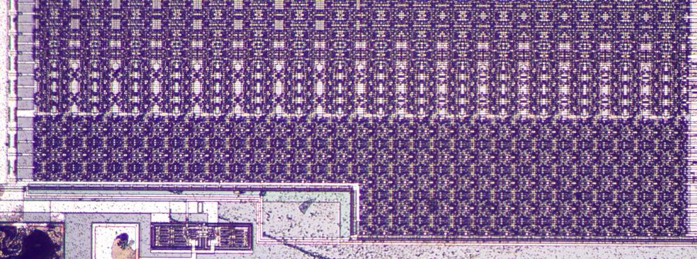
The photo below shows the bottom of the register file. The "notch" makes the registers at the very bottom half-width: 4 half-width rows corresponding to eight 16-bit registers. Since there are six 16-bit segment registers in the 386, I suspect these are the segment registers and two mystery registers.
I haven't been able to determine which registers in the 386 correspond to the other registers on the die. In the segment descriptor circuitry, there are two rows of register cells with ten more rows below, corresponding to 24 32-bit registers. These are presumably segment descriptors. At the bottom of the datapath, there are 10 32-bit registers with the T8 circuit. The 386's programmer-visible registers consist of eight general-purpose 32-bit registers (EAX, etc.). The 386 has various control registers, test registers, and segmentation registers8 that are not well known. The 8086 has a few registers for internal use that aren't visible to the programmer, so the 386 presumably has even more invisible registers. At this point, I can't narrow down the functionality.
Conclusions
It's interesting to examine how registers are implemented in a real processor. There are plenty of descriptions of the 8T static cell circuit, but it turns out that the physical implementation is more complicated than the theoretical description. Intel put a lot of effort into optimizing this circuit, resulting in a dense block of circuitry. By mirroring cells horizontally and vertically, the density could be increased further.
Reverse engineering one small circuit of the 386 turned out to be pretty tricky, so I don't plan to do a complete reverse engineering. The main difficulty is the two layers of metal are hard to untangle. Moreover, I lost most of the polysilicon when removing the metal. Finally, it is hard to draw diagrams with four layers without the diagram turning into a mess, but hopefully the diagrams made sense.
I plan to write more about the 386, so follow me on Twitter @kenshirriff or RSS for updates. I'm also on Mastodon occasionally as @[email protected].
Notes and references
-
Typically the write driver circuit generates a strong low on one of the bitlines, flipping the corresponding inverter to a high output. As soon as one inverter flips, it will force the other inverter into the right state. To support this, the pullup transistors in the inverters are weaker than normal. ↩
-
The pass transistor passes its signal through or blocks it. In CMOS, this is usually implemented with a transmission gate with an NMOS and a PMOS transistor in parallel. The cell uses only the NMOS transistor, which makes it worse at passing a high signal, but substantially reduces the size, a reasonable tradeoff for a storage cell. ↩
-
The bitline is typically precharged to a high level for a read, and then the cell pulls the line low for a 0. This is more compact than including circuitry in each cell to pull the line high. ↩
-
One problem is that the 386 uses a layer of insulating silicon oxynitride as well as the usual silicon dioxide. I was able to remove the oxynitride with boiling phosphoric acid, but this removed most of the polysilicon as well. I'm still experimenting with the timing; 20 minutes of boiling was too long. ↩
-
The image is an edited composite of multiple cells since the polysilicon was highly damaged when removing the metal layers. Unfortunately, I haven't found a process for the 386 to remove one layer of metal at a time. As a result, reverse-engineering the 386 is much more difficult than earlier processors such as the 8086; I have to look for faint traces of polysilicon and puzzle over what connections the circuit requires. ↩
-
You might wonder why they put two cells side-by-side instead of simply cramming the cells together more tightly. The reason for putting two cells in each row is presumably to match the size of each bit with the rest of the circuitry in the datapath. If the register circuitry is half the width of the ALU circuitry, a bunch of space will be wasted by the wiring to line up each register bit with the corresponding ALU bit. ↩
-
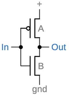
A CMOS inverter is constructed from an NMOS transistor (which pulls the output low on a 1 input) and a PMOS transistor (which pulls the output high on a 0 input), as shown below.
A CMOS inverter. -
The 386 has multiple registers that are documented but not well known. Chapter 4 of the 386 Programmers Reference Manual discusses various registers that are only relevant to operating systems programmers. These include the Global Descriptor Table Register (GDTR), Local Descriptor Table Register (LDTR), Interrupt Descriptor Table Register (IDTR), and Task Register (TR). There are four Control Registers CR0-CR3; CR0 controls coprocessor usage, paging, and a few other things. The six Debug Registers for hardware breakpoints are named DR0-DR3, DR6, and DR7 (which suggests undocumented DR4 and DR5 registers). The two Test Registers for TLB testing are named TR6 and TR7 (which suggests undocumented TR0-TR5 registers). I expect that these registers are located near the relevant functional units, rather than part of the processing datapath. ↩

5 comments:
The two extra segment registers could be LDTR and TR, both of which hold a 16-bit selector index from the GDT (technically bit 2 is always zero).
Hmm, I wonder how poorly sanding down the chip slowly would go...
even if uneven, if you take plenty of snapshots you might be able to find one that contains any part of the chip at any stage, then composite them together.
PS: F**K YOU recaptcha and you having to give me script permissions to google AND THINKING I'M A F*****G ROBOT!!1!11!
Hi Ken,
It seems the LOADALL instruction gives some hints about it. It has info on what registers are machine state and gives some info about invisible regs as well:
"The LOADALL instruction uses a 512-byte block of memory, where the lowest addressed byte is given in ES:[(E)DI]. The area above offset CC hex is used for processor dependent registers (temporaries, invisible registers). These are loaded into the processor, but will not affect normal program execution."
Moreover opcodes.lst from Ralf's brown list gives following:
...
D0H 30h Unused,not loaded
100H 4 Temporary Register IST
104H 4 Temporary Register I
108H 4 Temporary Register H
10CH 4 Temporary Register G
110H 4 Temporary Register F
114H 4 Temporary Register E
118H 4 Temporary Register D
11CH 4 Temporary Register C
120H 4 Temporary Register B
124H 4 Temporary Register A
As always thanks for a nice blog posts, it is always a joy!
Thanks,
Ruik
PS: my previous comment might be stuck in moderation or did not make it here. This is the second attempt, without any URLs.
> The six Debug Registers for hardware breakpoints are named DR0-DR3, DR6, and DR7 (which suggests undocumented DR4 and DR5 registers).
I don't think it suggests undocumented registers. The numbers in the names of the DR0..DR7 registers are simply the numbers used in the instruction encoding, specifically the three middle bits of the byte after the opcode in instructions that load or store those registers. Similarly, there are three control registers: CR0 has various important flags such as one that enables protected mode and one that enables paging; CR3 has the physical address of the top level of the hierarchical paging table; and CR2 is where the processor puts the effective address that caused a page fault so that the fault handler can examine it and eg. load the page from the hard disk. There is no CR1, and the digit in the name of the CR0..CR3 registers is used directly in the instruction encoding. (Pentium adds a CR4 register.)
Great post!
Interesting to hear that they used a P well for the NMOS transistors, I was under the impression that it was more common to use an N well for the PMOS transistors. (Or later, dual well). It depends on how the silicon without well is doped of course, but I think that transistors in a well that reverses the doping get somewhat worse performance than those without, so it depends on if you care more about performance of NMOS or PMOS transistors. Actually, since PMOS performs worse, it makes sense to me use a P well and even out the odds a little. But I'm sure that there are reasons to push the performance of your NMOS transistors too.
Post a Comment