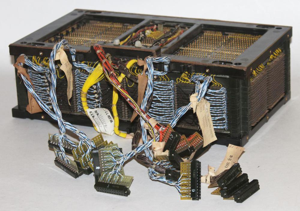
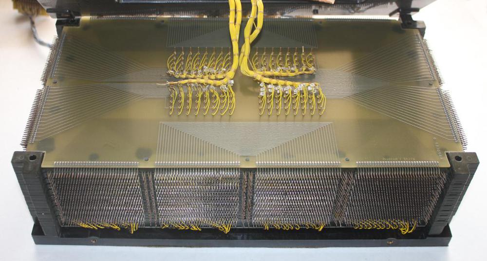
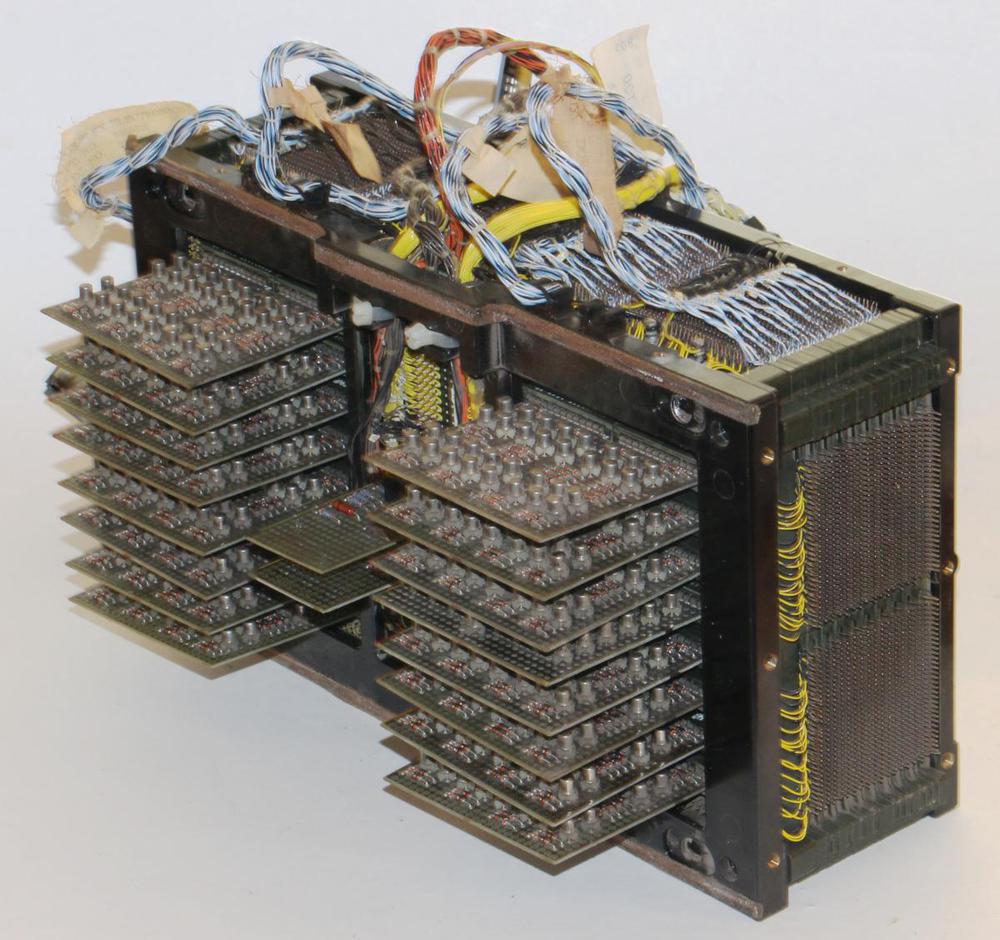
I recently received a vintage core memory array, part of an IBM System/360 mainframe computer. These arrays were used in a 128-kilobyte core memory system that filled a large cabinet weighing 610 pounds.1 This article explains how core memory worked, how this core array was used in mainframes, and why core memory was so bulky.
The IBM System/360 was a groundbreaking family of mainframe computers announced introduced in 1964, and much of the success of System/360 was due to core memory technology. The S/360 was an extremely risky "bet-the-company" project that cost IBM over $5 billion. The project was nearly derailed as the operating system OS/360 grew out of control: it was originally targeted for 16 KB systems, but grew to require 32 KB and then 64 KB. Fortunately, IBM was able to build larger core memories at a price that customers could still afford, so the operating system was usable.2 The System/360 project ended up being a huge success and ensured IBM's dominance of the computer industry for the next two decades. (For more about the System/360, see my recent article.)
How core memory worked
Core memory was the dominant form of computer storage from the 1950s until it was replaced by semiconductor memory chips in the early 1970s. Core memory was built from tiny ferrite rings called cores, storing one bit in each core. Each core stored a bit by being magnetized either clockwise or counterclockwise. A core was magnetized by sending a pulse of current through a wire threaded through the core. The magnetization could be reversed by sending a pulse in the opposite direction. Thus, each core could store a 0 or 1.
To read the value of a core, a current pulse flipped the core to the 0 state. If the core was in the 1 state previously, the changing magnetic field created a voltage in a sense wire. But if the core was already in the 0 state, the magnetic field wouldn't change and the sense line wouldn't pick up a voltage. Thus, the value of the bit in the core could be read by resetting the core to 0 and testing the tiny voltage on the sense wire. (An important side effect was that the process of reading a core erased its value so it needed to be rewritten.)
Using a separate wire for each core would be impractical, but in the 1950s a technique called "coincident-current" was developed that used a grid of wires to select a core. This depended on a special property of cores called hysteresis: a small current had no effect on a core, but a current above a threshold would magnetize the core. This allowed a grid of X and Y lines to select one core from the grid. By energizing one X line and one Y line each with half the necessary current, only the core where both lines crossed would get enough current to flip while the other cores were unaffected.
To store a word of memory, multiple core planes were stacked together, one plane for each bit in the word. The X and Y drive lines passed through all the core planes, selecting one bit of the word from each plane. Each plane had a separate sense line to read that bit.7 The IBM core stack below stored a 16-bit word along with two parity bits, so there were 18 core planes.
Writing to core memory required additional wires called the inhibit lines, one per core plane. In the write process, a current passed through the X and Y lines, flipping the selected cores (one per plane) to the 1 state, storing all 1's in the word. To write a 0 in a bit position, the plane's inhibit line was energized with half current, opposite to the X line. The currents canceled out, so the core in that plane would not flip to 1 but would remain 0. Thus, the inhibit line inhibited the core from flipping to 1.
To summarize, a typical core memory plane had four wires through each core: X and Y drive lines, a sense line, and an inhibit line. These planes were stacked to form an array, one plane for each bit in the word. By energizing an X line and a Y line, one core in each plane could be magnetized, either for reading or writing. The sense line was used to read the contents of the bit, while the inhibit line was used to write a 0 (by inhibiting the writing of a 1).
Some interesting features of the IBM core memory stack
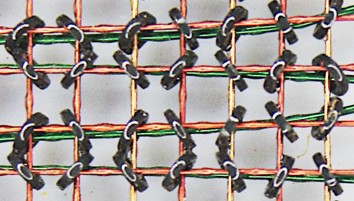
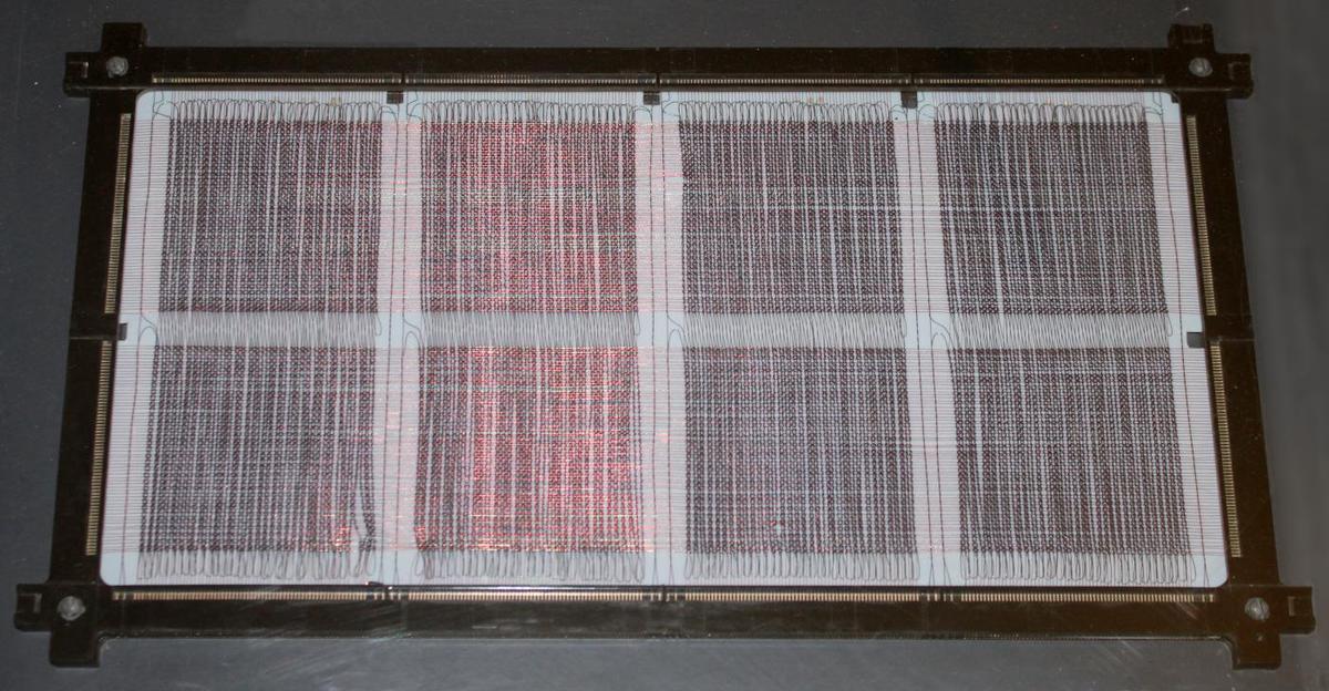
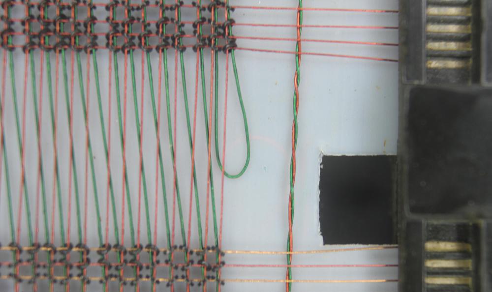
The IBM core memory I examined was fairly advanced, so there were some enhancements to the generic core memory described above. This core memory used the same wire for sense and inhibit, so there were three wires through each core instead of four, as you can see in the earlier closeup photo. This made manufacturing simpler, but complicated the circuitry. In addition, the core plane has some unusual features to reduce the amount of noise picked up by the sense wire, making it feasible to detect the tiny voltage in the sense wire. First, each plane had four sense/inhibit wires, not one. Since a sense wire only passed through 1/4 of the plane, it picked up less noise.7 In addition, the sense wire was shifted between the top half of the plane and the bottom half, so noise induced by an X line in one half would be canceled out in the second half. The photo below shows the sense wire (green) shifting over.
Each core plane in this memory array was rectangular, with 130 Y drive lines and 256 X drive lines. Since there was a core at each intersection, this yielded 33,280 cores. You might notice that this isn't a power of 2; the core plane held 32,768 cores for regular storage (32K) along with 512 extra cores for I/O storage. This extra storage was called "bump" storage. It was not part of the address space but was accessed through special circuitry.3
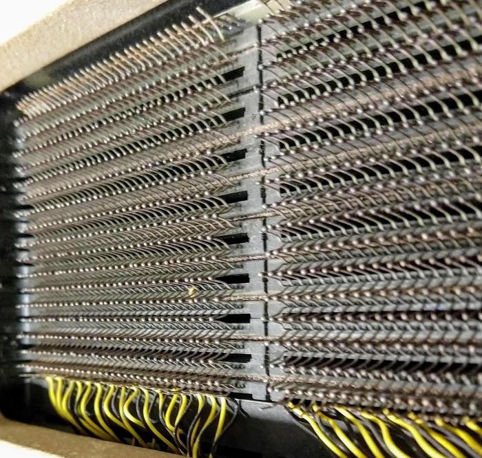
The X and Y drive lines in a core array pass through all the planes in the stack. Core arrays typically used jumper wires between the core planes, requiring a large number of soldered connections. One innovation in IBM's core memory design was to weld the planes together directly. Alternating pins along the edges of the plane were bent up or down and welded to the neighboring plane, simplifying manufacturing. This structure is shown in the photo below.
Systems using this core memory
I'll now take a detour to describe the systems that used this core array, and then discuss the circuitry that supported the array. IBM used several different core memory systems in the S/360 line. The core array in this article was used in the Model 40, Model 50, and the FAA's IBM 9020 air traffic control system.
IBM System/360 Model 40
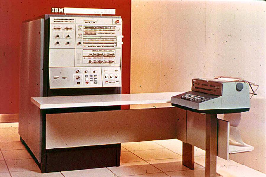
The Model 40 was a popular midrange computer for scientific and commercial applications and was one of IBM's most profitable computers. It typically rented for about $9,000-$17,000 per month and brought IBM over a billion dollars in revenue by 1972. To achieve better performance than the low-end models, the Model 40 used a two-byte datapath; the core memory system was designed to fetch two bytes at a time rather than one.
The IBM S/360 Model 40 was a compact system (for the time), with the computer in one frame known as the main frame. This frame held the circuit cards that make up the CPU, along with the power supplies, microcode (stored on metalized mylar sheets read by transformers), and core memory storage. (In contrast, large 360 systems might have dozens of frames.) The 128 KB core memory unit was mounted in the front right of the Model 40's frame, behind the console. The Model 40 could support an additional 128 KB of core memory, but this required a second storage frame, a five foot by two foot cabinet weighing 610 pounds.
IBM System/360 Model 50
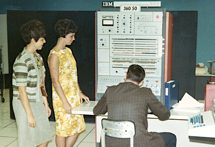
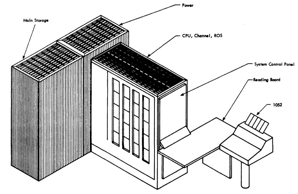
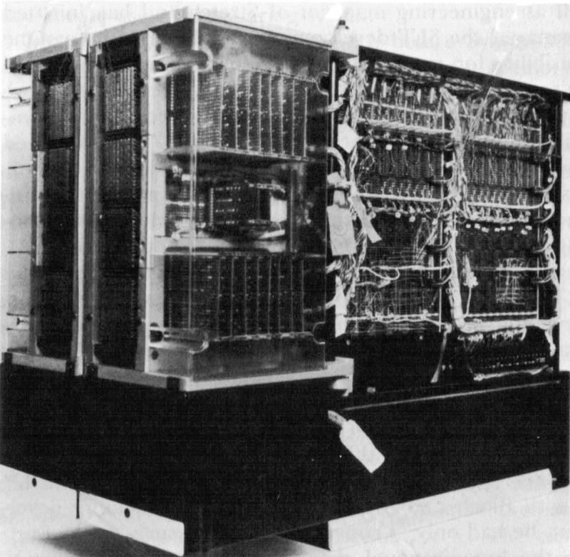
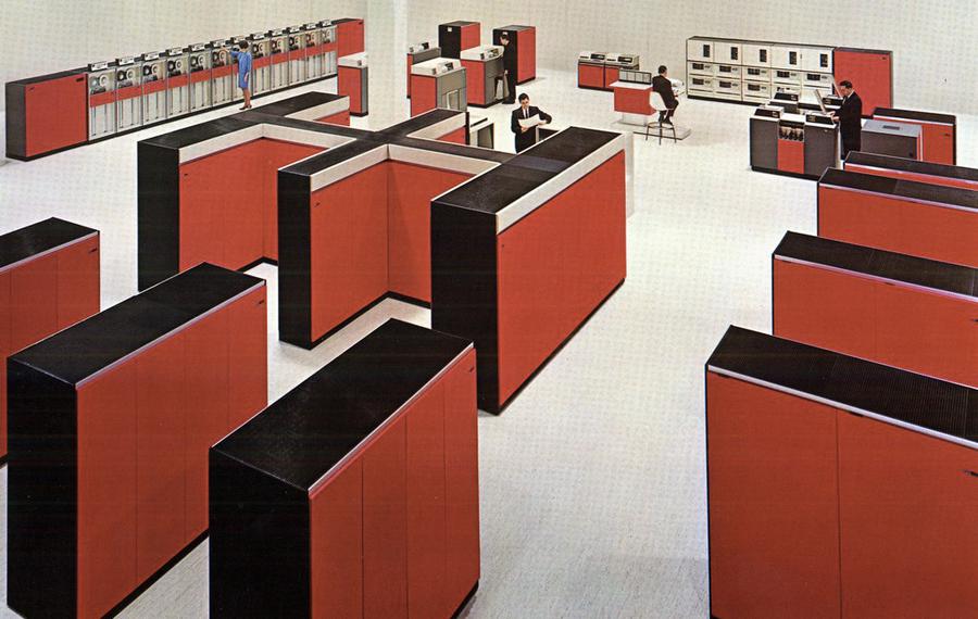
The Model 50 was a powerful mid-range machine in the System/360 lineup, significantly faster than the Model 40. The Model 50 typically rented for about $18,000 - $32,000 per month. The diagram below shows how the Model 50 consisted of three frames: the CPU frame (main frame) in front with the console, a power frame holding the power supplies, and the storage frame. In the photo above, the main frame is orange and about 2.5 feet wide by 5 feet deep. The power frame is the black cabinet behind the main frame, about 5 feet wide and 2 feet deep. The storage frame is the same size, on the left behind the women. The storage frame could hold up to 256 KB; by adding a second storage frame behind it, the Model 50 could be expanded to 512 KB.
The FAA's IBM 9020 multiprocessor system
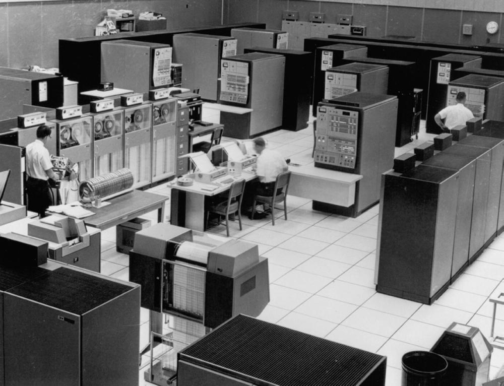
The core memory array I examined was from an air traffic control system called the IBM 9020. In the mid-1960s, the FAA realized that computerization was necessary to handle increased air traffic. From the early 1970s to the 1990s, the FAA used the IBM 9020 to track flights and integrate radar data. The 9020 was a multiprocessor system designed for reliability, consisting of up to 12 mainframes connected together, driving dozens of air traffic displays (the classic round CRT displays). The system used modified Model 65 computers to process data and used modified Model 50 computers for I/O control (essentially expensive DMA controllers).4
The complete core memory system
The stack of core planes isn't enough to implement a working memory; a lot of circuitry is required to generate the appropriate X and Y signals, amplify the sense line signals for reads, and drive the inhibit lines for writes. In this section, I explain how the stack of core memory planes was used as part of a full memory system.
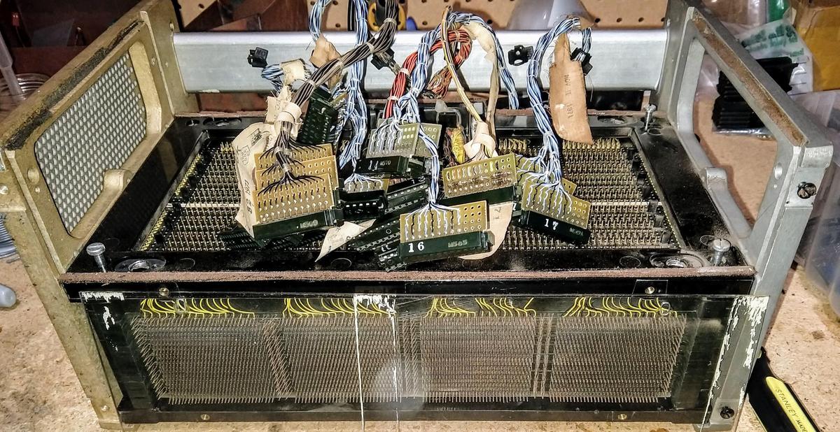
Each X and Y line through the core plane required two transistor drivers, one to generate the current pulse for reading and one to generate the opposite current pulse for writing. Thus, with 128 X lines and 128 Y lines,5 a total of 512 drive transistors were required, a very large number of transistors. These were provided by 16 "driver gate" cards, each with 32 drive transistors, plugged into each core stack.10 The photo below shows the 16 driver gate boards (each with 32 transistors) plugged into the core array.
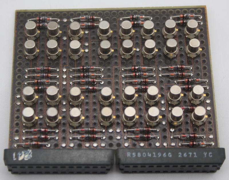
The photo below shows a closeup one of the transistor "driver gate" cards, with a transistor and diode for each line.6 Cards like this with discrete transistors were unusual in the IBM System/360, which for the most part used SLT modules, hybrid modules somewhat like integrated circuits.
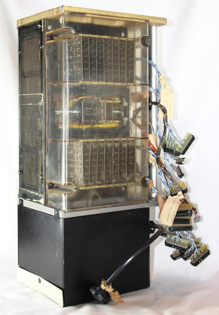
The core array and the drive transistors generated significant heat so the assembly was cooled by a fan mounted underneath. Plastic covers over the boards directed the airflow, as well as providing protection for the boards. The photo below shows the core memory mounted on a metal frame with the fan attached.
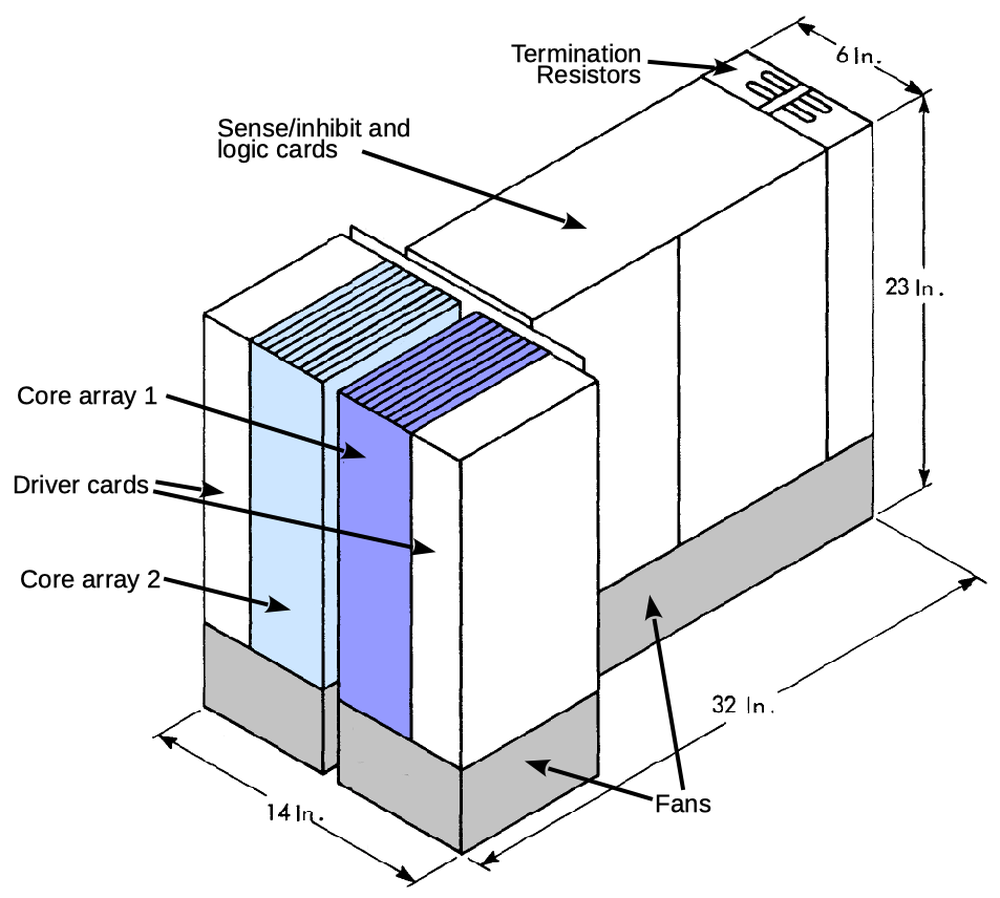
The photo below shows the 128 KB unit, consisting of two core arrays (on the left), along with about 62 small circuit cards of supporting circuitry. This unit was rather bulky, almost three feet long and two feet high.8 Over half of these circuit cards were sense preamplifiers to read the weak signals from the core planes.7 Other cards decoded the address to select the right lines9, handled timing, or did other tasks. The slower Model 40 computer accessed one of the two arrays at a time, reading 16 bits (a half-word). In contrast, the Model 50 accessed both arrays in parallel, reading a full 32-bit word at once for higher performance.
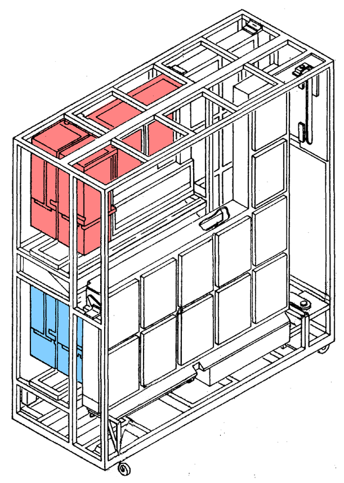
The diagram below shows how two of these core memory units (i.e. four stacks of 18 planes) were installed in the Model 50's storage frame, providing 256 kilobytes of storage. This frame was about 5 feet by 2 feet and 6 feet tall and weighed 1150 pounds. The storage frame also held the optional "storage protect" feature, that protected memory blocks from access by other programs. Note that even though the core planes themselves were fairly compact, the entire storage frame was rather large. This diagram also illustrates why the cabinets were called frames: it was built from a frame of metal bars with side panels hung off the frame to enclose it.
Other IBM S/360 memory systems
I've described the core memory used in the Model 40 and Model 50, but high-end models used even larger core memory systems based on different core planes. The photo below shows a high-performance Model 85 system. The four cabinets in front are IBM 2365 Processor Storage; each one held 256 kilobytes of core memory and weighed over a ton. High-end systems could also use the 2385 Processor Storage holding 2 megabytes of memory in a sprawling 400 square foot unit that weighed almost 8 tons. The IBM 2361 Large Capacity Storage (LCS) also held 2 megabytes; it was slower but weighed just one ton. It used large 4-foot core planes that looked more like screen doors than typical core planes.1
Conclusion
Computers in the early 1950s used memory technologies such as mercury delay lines and Williams tubes that were small and slow. Core memory was much superior and it led to the rise of the computer era in the late 1950s and 1960s. As manufacturing technology improved, the price of core memory rapidly dropped, from several dollars per bit to a penny per bit. By 1970, IBM was producing over 20 billion cores per year.
However, even with its steady improvements, core memory was not able to survive the introduction of integrated circuits and semiconductor memory in the late 1960s. In 1968, IBM switched its development efforts from core memory to semiconductor memory. This led to the introduction in 1971 of the world's first commercial computer with semiconductor memory, the IBM S/370 Model 145. The capacity of integrated circuit memories grew exponentially as their price fell, as described by Moore's law. As a result, semiconductors took over the memory market from magnetic cores by the end of the 1970s. Now, thanks to DRAM memories, modern computers have memory measured in gigabytes rather than kilobytes and memory comes in a small DIMM module rather than a large cabinet.
I announce my latest blog posts on Twitter, so follow me @kenshirriff for future articles. I also have an RSS feed. I've written before about core memory in the IBM 1401 and core memory in the Apollo Guidance Computer. Thanks to Robert Garner for supplying the core array. Thanks to Gio Wiederhold and Marianne Siroker for research assistance.
More information
In the video below, Marc, Carl, and I wired up a different type of IBM core memory plane and manually read and wrote a bit. It was harder than we expected; the signal from a flipping core is very small and hard to distinguish from noise.
The book Memories That Shaped an Industry describes the history of core memory in detail, with a focus on IBM. The book IBM's 360 and early 370 systems thoroughly describes the history of the S/360. The memory system used in the System/360 Model 40 is explained in Model 40 Functional Units, page 141 onwards. See ibm360.info for documents on the FAA's IBM 9020 system.
Notes and references
-
The weight of additional memory depended on the computer model. For the Model 40, adding 128K to get the "H" configuration requires the addition of Frame 2, weighing 610 pounds. For the Model 50, the first 256K ("H" configuration) fit in Frame 2 (1150 pounds), while the next 256K ("I" configuration) required the addition of Frame 4, which weighed 1500 pounds. So, depending on the particular computer, 128K weighed 575, 610, or 750 pounds. For details, see the physical planning guide, which provides the dimensions and weight of the various S/360 components. ↩
-
The book Memories That Shaped an Industry discusses how IBM's leadership in core memory development made the IBM System/360 possible. IBM's near-disaster in developing software for the S/360 led to the legendary book The Mythical Man-Month by Fred Brooks, who managed development of the S/360 hardware and operating system. ↩
-
Each core planes used in the Model 40 and 50 computers had an extra 512 bits of "bump" storage. This extra storage held information on I/O operations (the "unit control word") without using the main storage. The computers also had "local storage", a separate small core storage used for registers. ↩
-
The computers used in the IBM 9020 system were based on the S/360 Model 50 and Model 65, but had modifications to operate in a networked high-availability system. For instance, most console controls were disabled except during maintenance to avoid accidental button presses. The computers also included address translation so they could access multiple shared external storage units, allowing failover of storage. The Model 65's instruction set was extended with highly specialized instructions such as CVWL (convert weather lines) that converted weather data coordinates for the displays, as well as instructions for multiprocessing. (Details in FETOM.)
The IBM 9020 network architecture, using Model 50 computers as I/O controllers connected to Model 65 computers, may seem pointlessly complex. It turns out that is the case. According to Brooks, IBM originally designed a reasonable FAA system with just Model 50 computers. However, the (somewhat arbitrary) design specification created by MITRE required separate processing and I/O tiers in the network, so IBM added the Model 65 computers even though they were unnecessary and made the system less reliable. ↩
-
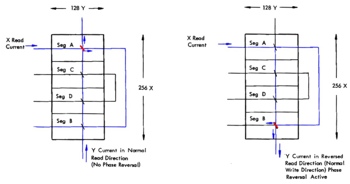
The core plane had 256 X lines and 130 Y lines, but the circuitry drove 128 X lines and 128 Y lines, so you might wonder why the numbers don't match. There are two factors here. First, a technique called "phase reversal"11 used each X line twice, in opposite directions, so the 256 physical X lines through the core plane only required 128 X drivers, reducing the amount of drive hardware required. Second, the 2 extra Y lines for bump storage were driven by separate circuitry. ↩
-
An X or Y line was connected to a read gate card at one end, and a write gate card at the other end; these lines had a high-current (360 mA) pulse for 400-700 nanoseconds to flip a core. The current path through a line was as follows: the +60V supply was connected through a terminating resistor to a "terminator gate", a transistor that controlled the timing. Then through the diode on a gate card, through the cores, and through a transistor on the gate card at the other end. Finally, the current passed through a driver card to ground. (The gate card is the card full of transistors plugged directly into the array while the driver card does part of the address decoding.) The memory system is explained in Model 40 Functional Units, page 141 onwards. ↩
-
One unusual feature of this core plane is that it had four separate sense/inhibit lines, each covering 1/4 of the plane. This reduced the length of each sense line and thus reduced the noise it picked up, but required four times as many amplifiers to read the sense lines. Since there were 18 planes (18 bits) in the core array, 72 sense pre-amplifiers were required for each of the two core arrays. The pre-amplifiers were differential amplifiers, amplifying the difference between the two sense line inputs. (The idea is that noise on both inputs will cancel out, yielding just the desired signal.) The outputs from all the pre-amplifiers were fed into 18 "final amplifiers" yielding the 18-bit output (2 bytes + 2 parity bits) from the array. The sense and inhibit lines were shared in this core plane, so there also 72 inhibit lines. One circuit card implemented both the sense preamp and the inhibit driver for 4 lines, so the two stacks of core planes required 36 Sense Preamp and Z [i.e. inhibit] Driver cards. ↩
-
The diagram below shows the dimensions of the 128 KB core memory unit, containing two sets of core planes. Each colored block is a core array of 18 planes, corresponding to the array shown at the beginning of this article.
The 128 KB core memory unit contained two arrays and was almost three feet long. -
The Model 50 core unit with two core arrays held 128 kilobytes as 32K words of 32 bits plus parity. Addressing one of 32K words required 15 address bits, decoded as follows. For X, 4 bits selected one of 16 "gate decoder lines" and 3 bits selected one of 8 "drivers". These two selections were combined in the transistor matrix to select one of the 128 X drive lines. The Y address was decoded similarly, with 7 bits selecting one of 128 Y lines. One bit controls "phase reversal", selecting the polarity of the Y drive line. Although the System/360 was byte-addressable, accessing a specific byte in a word was done by the processor, rather than by the memory system. Because the Model 40 read half-words at a time from memory, it used a slightly different decoding scheme. One address bit was used to select between the two core arrays in the unit and only one array was accessed at a time. ↩
-
Each gate driver card had 32 transistors in a grid, with 8 inputs to transistor emitters and 4 inputs to transistor bases. By activating one base input and one emitter input, the corresponding transistor turned on, energizing the corresponding line. Thus, each card allowed 32 lines to be controlled by selecting one of 4 inputs, and one of 8 inputs. Each card also had 32 diodes that provided the current into the appropriate line. If a transistor was activated, the diode on the card connected to the opposite end of the line sourced the current. ↩
-
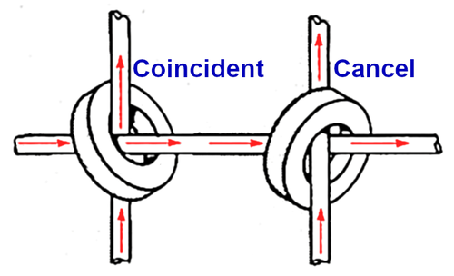
One subtlety of the coincident-current design is that if the wires pass through the core in opposite directions, the currents subtract instead of add. In the diagram below, the wires pass through the left core in the same direction so the currents coincide. But in the right core, the wires pass through in opposite directions, so the currents cancel out. This is important because neighboring cores are rotated 90° to prevent magnetic coupling. In order for currents to coincide, the direction of current must be reversed in every other line. To accomplish this reversal, lines through the core stack were wired alternating bottom-to-top versus top-to-bottom.
If currents pass through a core in the same direction, they add. This is the principle behind "coincident-current" core memory. However, if currents pass through a core in opposite directions (as on the right), the currents cancel.The "phase reversal" technique used this cancellation to cut the number of X drive lines in half for this core memory plane. The trick was to run the X lines through half of the core plane normally, and then through the other half of the core plane "backward". When an X line and a Y line are activated, two cores will receive both X and Y currents. But only one of these cores will receive the currents in the same direction and will flip; for the other core, the currents will cancel out. On the other hand, by reversing the current through the Y line, the opposite cancellation will occur and the other core will be selected. Thus, phase reversal allows the system to support twice as many cores with essentially the same driver hardware, just switching the Y current direction as needed.
On the left, the coincident currents select a core in segment A. By reversing the direction of the Y current, a core in segment B is selected instead. With this phase reversal technique, one wire went through two X rows. Diagram based on Model 40 Functional Units page 147.
20 comments:
We used this stuff in the USN because it was supposed to be EMP proof.
Nitpick: you wrote “33,280 cores. You might notice that this isn't a power of 2; the core plane held 32,768 cores for regular storage (32K) along with 1024 extra cores for I/O storage.” That math is incorrect. It’s only 512 extra cores.
Anonymous: yes, you are correct.
Wow so i have over 50 million kg worth of memory in my laptop :)
I must be getting old.I can remember correctly memories, card punch machines and the massive power supplies.
Programs were hand written and passed to a young lady to feed into the computer with toggle switches.
Quote of the day... Only an optimist programs in ink.
That should of course read core memories...
Great article! There's a very interesting paper on how IBM manufactured core memories here (pdf).
An interesting detail is that core planes were threaded and tested a line at a time: if there is a bad or missing core, it can be crushed and redone.
There's also a good thread with lots of detail and images of cores here.
I worked at Digital Equipment in the 80's (PDP-11's, VAX, then Alpha). Many PDP-11's were purchasable with core memory and used in dedicated applications. Some customers liked them because the OS could detect impending power loss and quickly store CPU state into core as well as safe the core array. When power returned the PDP-11 could nearly instantly resume exactly where it left off - because the core memory is non-volatile. This helped immensely in some applications. The headquarters in Maynard MA where I worked had a small core memory museum. There were pictures of women in a huge area hand stringing the core arrays under magnifiers. Arrays were tested after stringing, and if they failed would be diagnosed and repaired. It took a lot of labor to string the cores. the museum had a small evolution of core display. I hope that was preserved! I have a core memory board in my office on my history wall that I salvaged from a dumpster when they were purging the labs. Our college coops are astonished how little memory is stored on the 12"x12" H214 card (it's 8192x16 bits).
Great as always. One thing I don't quite get is what the second input to the differential sense amplifier is. Is it just one of the other sense lines, from another set of cores (that would sort of make sense, as those cores are not being read you would just pick up the common mode noise, at least assuming they're near each other)?
Julien, to simplify a bit, the sense line is a loop going through all the cores. The two ends of the loop are connected to the differential sense amplifier. The core's pulse will be positive on one end and negative on the other, while induced noise will hopefully be the same on both ends of the wire. A tricky part is to wire the sense line so you don't pick up the pulses on the X and Y lines. Many core planes use a diagonal sense wire so it won't get an induced signal. The IBM plane shifts the sense wire so the top half picks up the X noise with opposite polarity from the bottom half and it cancels out.
Ah, thanks Ken, I didn't think it would actually be the two ends of the same sense wire, but now it makes sense. As for picking up the pulses from X/Y, I ran into the same problem when building a single bit of core memory (inspired by your last article on it). I fixed it using the same principle, though because I only had one bit, I actually added two cores with only half the read/write current each (kind of like just X and just Y respectively, only that it's not really X/Y with a single bit), and the sense line going through in the opposite direction.
I started as an IBM 1401 Autocoder programmer in 1963 working for Anglo American Corporation in Kitwe, Northern Rhodesia now Zambia. I was 17 years old, had a Grade 9 education, loved math and aced the IBM aptitude test :) ...
Shortly after we upgraded to an IBM 1410 followed by an IBM 1440.
I came to Canada as a 19 year old all by myself and joined General Foods (Kraft) in Toronto in 1966. When I retired in 2006 I was the Director, Academic Computing for St Thomas university. Never went back to school to get my high school diploma lol.
I believe core memory also required delay lines. I joined in 1978 when the 370 and 43xx systems were going strong, but there were still a lot of 360 systems in use. I remember the older guys needing to tune delay lines. Was let go during a downturn and went on to get an MSCS degree in CompSci. Now I am a Java and Salesforce (cloud computing) lead developer at a major finance company.
Would like to hear more details about the Xerox Alto implementation. Did you use any microcode when writing it? Nice to see that the Alto is still alive, I haven't thought about it for many years (since my days at U of R and Xerox). I did write a microcode compiler for it back then. You may try to find out if the code still exists. It would help for projects like this.
REPAIRING 360/370 MAINFRAME AND IBM TRANSISTOR COMPUTERS:
THE CONSOLE LIGHTS WERE ESSENTIAL TO REPAIR AN 1BM 360/370/system 3 NOT JUST COSMETIC!
Ibm had a very sophisticated schematic system to trace faults and shorts in a 360/370
system 3 computer. The logics/ schematics to trace thousands of wire wrapped connections
and thousands of pc cards were called IBM MAPS.
The maps relied on the ce stepping thru the instruction set and displaying the results
on the console lights as bits going in and out of memory and the registers.
1) MOST PROBLEMS WERE CAUSED BY OVER HEATING, THE AIR CONDITIONING ON A HOT DAY WOULD BE
fail to cool the machine!
2) contacts on the slt cards were a major problem: the fix was usually finding a card
out of hundreds(using the MAPS) then cleaning the contacts and replugging the card!
IBM's original solution to the contact problem was to use very heavy gold or palladium
plating on the contacts of slt cards( usually $2,000 to $20,000 dollars worth of gold
per machine).
The gold solution was not a great solution!
IBM finally solved the contact problem on the IBM PC by just screwing the cards into
the socket with a 2 cent screw! Every PC maker following this solution!
As far as the Columbia university 360/91, a scrap/ gold dealer from south Dakota
dismantled the machine and sold us several hundred slt cards and disk drive heads.
We had a computer leasing and used computer business at the time and used the parts
to maintain system 3's, 360 40 and 50's, 370 135 145.
The biggest problem with IBM machines were Disk head crashes, not CARD FAILURE!
on IBM machines most failures just required replugging the card!
On DEC and Data General computer that we maintained for customers the problems were
shorting of cards and complete failure of memory or cpu boards(each costing thousands of dollars!)
TRANSISTOR MACHINES: We had both RCA 301's and ibm 1440's in our service bureau and
contracts to maintain IBM 1440 and 1460's. These were very reliable machines except
for the IBM disk drives and the printers on the RCA and IBM 1440's
With the IBM diagrams. I could fix a 1440 in 3 hrs, using a traditional wiring diagrams
that RCA(univac) used it would take 1 to 3 days!
In our experience IBM machines had very good reliability EXCEPT for the disk drives
that failed all the time!!!
I am glad to see that modern hard drive technology has improved the failure rates of
hard drivers, a problem that IBM never solved!
We have the control panel from the FAA system on display at the Stanford CS historic displays,
see http://infolab.stanford.edu/pub/voy/museum/pictures/display/3-1.htm.
I just come across your web page when trying to validate information for my autobiography, soon to be available at Wiederhold.org/Stories/GioWiederhold1936.pdf, where I describe a.o. the IBM 360-50 installation in 1966 at the Stanford Medical school. It included both a 2361 megabyte memory and a 2321 datacell drive.
I've played with making a capacitor+neon bulb DRAM planes for a relay computing project. Still got a bunch of soldering to do for it, but it was very much core-inspired.
PROM in the "neon technology" is a matrix of neon bulbs in tiny sockets. Install one and it's a logic 1, remove it and it's a logic 0. When a film capacitor is added in series with the neon, it stores state. A readout changes the polarity of some of the capacitors, causing a current to flow - equivalent to a change in magnetization of a magnetic core. A reed relay coil at the bottom of each column acts as a sense amplifier. Readout is destructive :)
5mm neon bulbs have high enough impedance to drive a 1-2kOhm sense coil, typical of 12-24V reed relays, without breaking down into an arc. The drive voltage level for reliable readout is somewhat temperature dependent, but much less than the temperature dependency of core plane operating point.
Another great blog, Ken. Just a small correction regarding your picture of the Jacksonville 9020, as I know you strive for accurate detail. The three mainframes along the left wall are not Model 65s. All six mainframes in the picture are modified Model 50s (known as 7201-01s). Jacksonville initially had a 9020A as pictured but was soon upgraded to a 9020D, which is possibly what misled you. It was the 9020D that incorporated three modified Model 65s (7201-02s). The 9020 Model 65 is easily identified by its additional Dynamic Address Translation frame, which makes it physically much larger. The standard Model 65 did not have this frame and was the same size as the Model 50. See this drawing from the 7201-02 Parts Catalog www.ibm360.info/Misc/DATFrame.JPG
I recall from the late 1960s that IBM had the memory shipped out to Spain for the diagonals wires to be threaded. This was because there were many women skilled in lace making who had the dexterity to thread the wires. Was that correct?
A wealth of information in this article - thank you.
They were sent to Portugal
Post a Comment