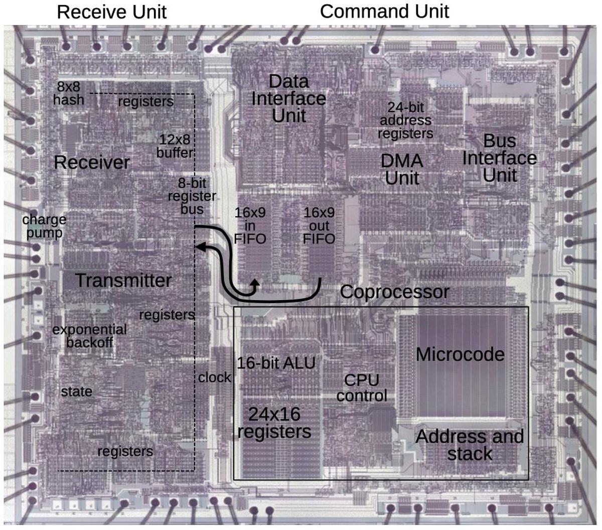
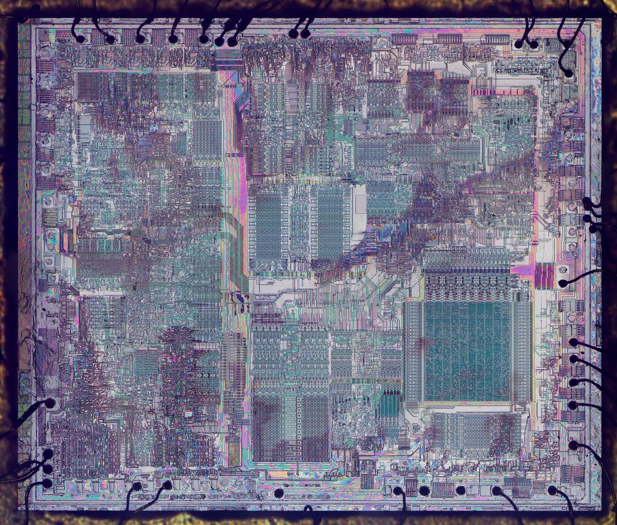
The die photo below shows the i82586 chip. This photo shows the metal layer on top of the chip, which hides the underlying polysilicon wiring and silicon transistors. Around the edge of the chip, square bond pads provide the link to the chip's 48 external pins. I have labeled the function blocks based on my reverse engineering and published descriptions. The left side of the chip is called the "receive unit" and handles the low-level networking, with circuitry for the network transmitter and receiver. The left side also contains low-level control and status registers. The right side is called the "command unit" and interfaces to memory and the main processor. The right side contains a simple processor controlled by a microinstruction ROM.1 Data is transmitted between the two halves of the chip by 16-byte FIFOs (first in, first out queues).
The 82586 chip is more complex than the typical Ethernet chip at the time. It was designed to improve system performance by moving most of the Ethernet processing from the main processor to the coprocessor, allowing the main processor and the coprocessor to operate in parallel. The coprocessor provides four DMA channels to move data between memory and the network without the main processor's involvement. The main processor and the coprocessor communicate through complex data structures2 in shared memory: the main processor puts control blocks in memory to tell the I/O coprocessor what to do, specifying the locations of transmit and receive buffers in memory. In response, the I/O coprocessor puts status blocks in memory. The processor onboard the 82586 chip allows the chip to handle these complex data structures in software. Meanwhile, the transmission/receive circuitry on the left side of the chip uses dedicated circuitry to handle the low-level, high-speed aspects of Ethernet.
Ethernet and collisions
A key problem with a shared network is how to prevent multiple computers from trying to send data on the network at the same time. Instead of a centralized control mechanism, Ethernet allows computers to transmit whenever they want.3 If two computers transmit at the same time, the "collision" is detected and the computers try again, hoping to avoid a collision the next time. Although this may sound inefficient, it turns out to work out remarkably well.4 To avoid a second collision, each computer waits a random amount of time before retransmitting the packet. If a collision happens again (which is likely on a busy network), an exponential backoff algorithm is used, with each computer waiting longer and longer after each collision. This automatically balances the retransmission delay to minimize collisions and maximize throughput.
I traced out a bunch of circuitry to determine how the exponential backoff logic is implemented. To summarize, exponential backoff is implemented with a 10-bit counter to provide a pseudorandom number, a 10-bit mask register to get an exponentially sized delay, and a delay counter to count down the delay. I'll discuss how these are implemented, starting with the 10-bit counter.
The 10-bit counter
A 10-bit counter may seem trivial, but it still takes up a substantial area of the chip. The straightforward way of implementing a counter is to hook up 10 latches as a "ripple counter". The counter is controlled by a clock signal that indicates that the counter should increment. The clock toggles the lowest bit of the counter. If this bit flips from 1 to 0, the next higher bit is toggled. The process is repeated from bit to bit, toggling a bit if there is a carry. The problem with this approach is that the carry "ripples" through the counter. Each bit is delayed by the lower bit, so the bits don't all flip at the same time. This limits the speed of the counter as the top bit isn't settled until the carry has propagated through the nine lower bits.
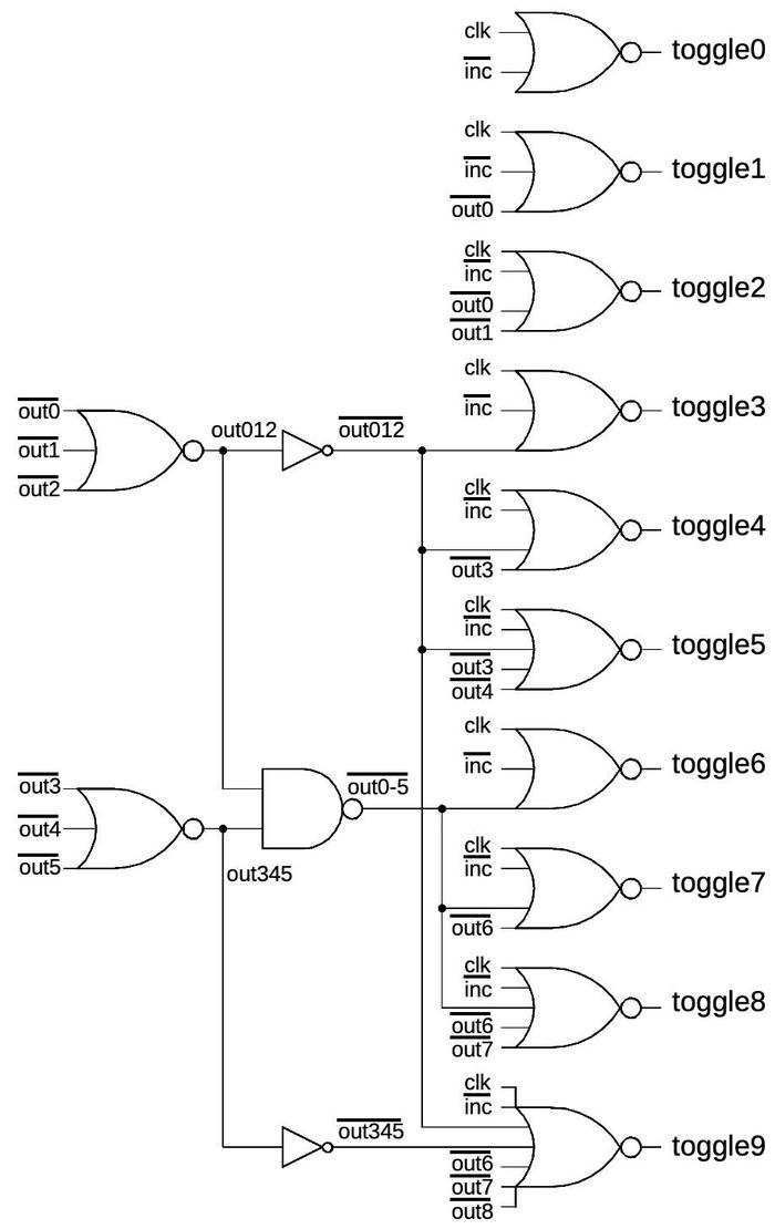
The counter in the chip uses a different approach with additional circuitry to improve performance. Each bit has logic to check if all the lower bits are ones. If so, the clock signal toggles the bit. All the bits toggle at the same time, rapidly incrementing the counter in response to the clock signals. The drawback of this approach is that it requires much more logic.
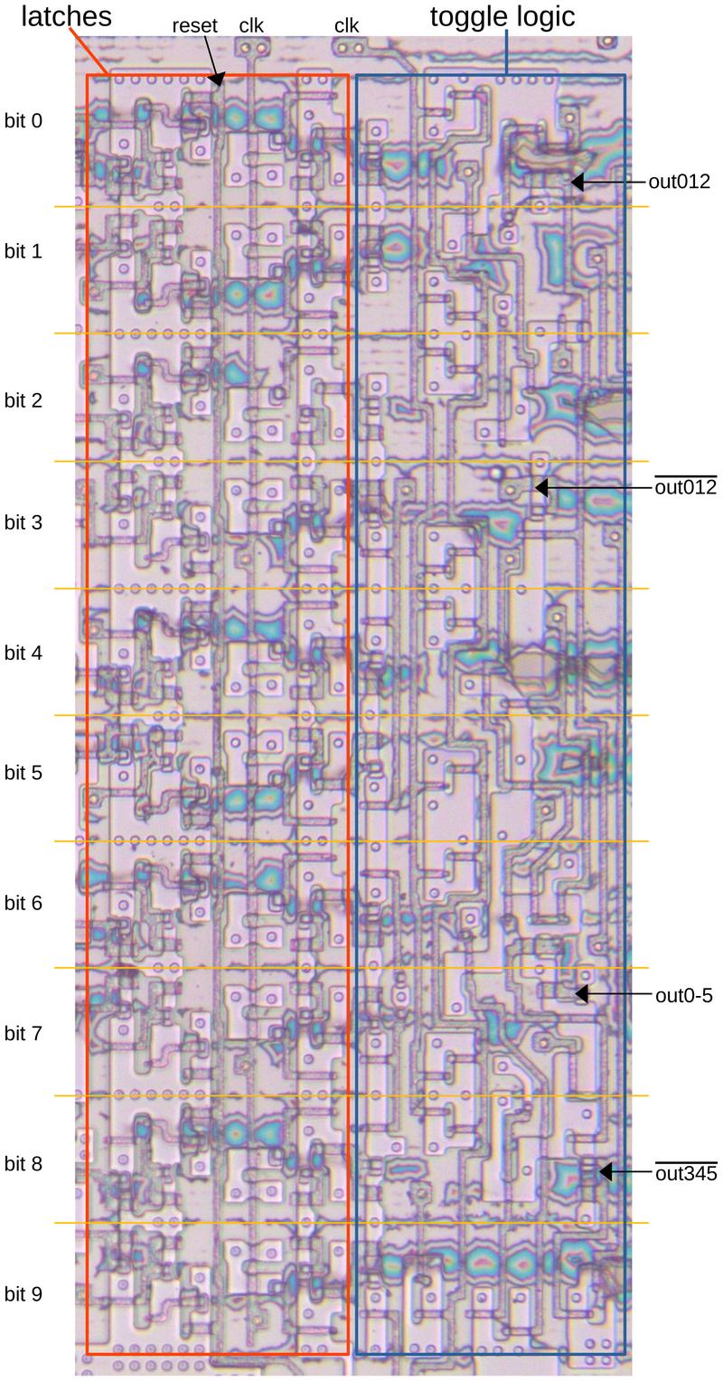
The diagram below shows how the carry logic is implemented. The circuitry is optimized to balance speed and complexity. In particular, bits are examined in groups of three, allowing some of the logic to be shared across multiple bits. For instance, instead of using a 9-input gate to examine the nine lower bits, separate gates test bits 0-2 and 3-5.
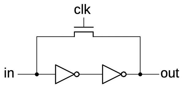
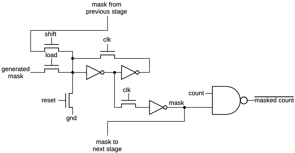
The implementation of the latches is also interesting. Each latch is implemented with dynamic logic, using the circuit's capacitance to store each bit. The input is connected to the output with two inverters. When the clock is high, the transistor turns on, connecting the inverters in a loop that holds the value. When the clock is low, the transistor turns off. However, the 0 or 1 value will still remain on the input to the first inverter, held by the charge on the transistor's gate. At this time, an input can be fed into the latch, overriding the old value.
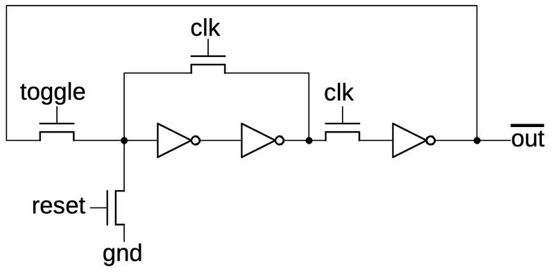
The latch has some additional circuitry to make it useful. To toggle the latch, the output is inverted before feeding it back to the input. The toggle control signal selects the inverted output through another pass transistor. The toggle signal is only activated when the clock is low, ensuring that the circuit doesn't repeatedly toggle, oscillating out of control.
The image below shows how the counter circuit is implemented on the die. I have removed the metal layer to show the underlying transistors; the circles are contacts where the metal was connected to the underlying silicon. The pinkish regions are doped silicon. The pink-gray lines are polysilicon wiring. When polysilicon crosses doped silicon, it creates a transistor. The blue color swirls are not significant; they are bits of oxide remaining on the die.
The 10-bit mask register
The mask register has a particular number of low bits set, providing a mask of length 0 to 10. For instance, with 4 bits set, the mask register is 0000001111. The mask register can be updated in two ways. First, it can be set to length 1-8 with a three-bit length input.5 Second, the mask can be lengthened by one bit, for example going from 0000001111 to 0000011111 (length 4 to 5).
The mask register is implemented with dynamic latches similar to the counter, but the inputs to the latches are different. To load the mask to a particular length, each bit has logic to determine if the bit should be set based on the three-bit input. For example, bit 3 is cleared if the specified length is 0 to 3, and set otherwise. The lengthening feature is implemented by shifting the mask value to the left by one bit and inserting a 1 into the lowest bit.
The schematic below shows one bit of the mask register. At the center is a two-inverter latch as seen before. When the clock is high, it holds its value. When the clock is low, the latch can be loaded with a new value. The "shift" line causes the bit from the previous stage to be shifted in. The "load" line loads the mask bit generated from the input length. The "reset" line clears the mask. At the right is the NAND gate that applies the mask to the count and inverts the result. As will be seen below, these NAND gates are unusually large.
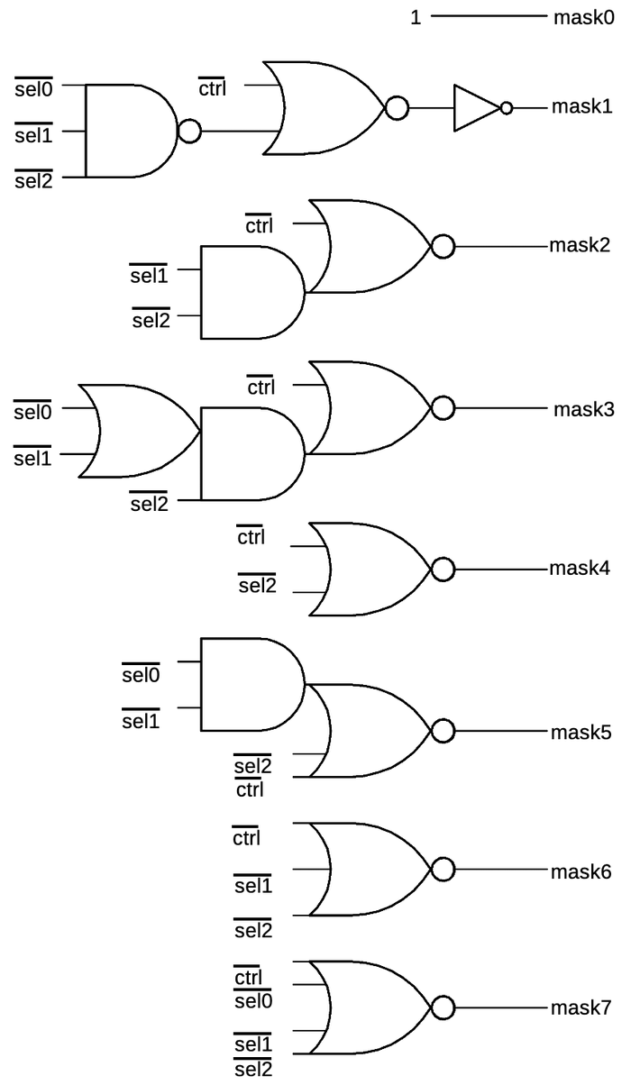
The logic to set a mask bit based on the length input is shown below.6 The three-bit "sel" input selects the mask length from 1 to 8 bits; note that the mask0 bit is always set while bits 8 and 9 are cleared.7 Each set of gates energizes the corresponding mask line for the appropriate inputs.
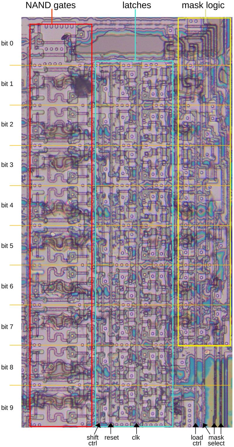
The diagram below shows the mask register on the die. I removed the metal layer to show the underlying silicon and polysilicon, so the transistors are visible. On the left are the NAND gates that combine each bit of the counter with the mask. Note that large snake-like transistors; these larger transistors provide enough current to drive the signal over the long bus to the delay counter register at the bottom of the chip. Bit 0 of the mask is always set, so it doesn't have a latch. Bits 8 and 9 of the mask are only set by shifting, not by selecting a mask length, so they don't have mask logic.8
The delay counter register
To generate the pseudorandom exponential backoff, the counter register and the mask register are NANDed together. This generates a number of the desired binary length, which is stored in the delay counter. Note that the NAND operation inverts the result, making it negative. Thus, as the delay counter counts up, it counts toward zero, reaching zero after the desired number of clock ticks.
The implementation of the delay counter is similar to the first counter, so I won't include a schematic. However, the delay counter is attached to the register bus, allowing its value to be read by the chip's CPU. Control lines allow the delay counter's value to pass onto the register bus.
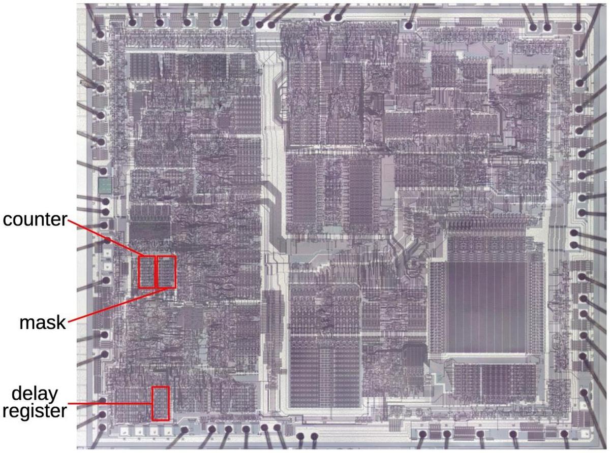
The diagram below shows the locations of the counter, mask, and delay register on the die. In this era, something as simple as a 10-bit register occupied a significant part of the die. Also note the distance between the counter and mask and the delay register at the bottom of the chip. The NAND gates for the counter and mask required large transistors to drive the signal across this large distance.
Conclusions
The Intel Ethernet chip provides an interesting example of how a real-world circuit is implemented on a chip. Exponential backoff is a key part of the Ethernet standard. This chip implements backoff with a simple but optimized circuit.9
For more chip reverse engineering, follow me on Twitter @kenshirriff or RSS for updates. I'm also on Mastodon occasionally as @[email protected]. Acknowledgments: Thanks to Robert Garner for providing the chip and questions.
Notes and references
-
I think the on-chip processor is a very simple processor that doesn't match other Intel architectures. It is described as executing microcode. I don't think this is microcode in the usual sense of machine instructions being broken down into microcode. Instead, I think the processor's instructions are primitive, single-clock instructions that are more like micro-instructions than machine instructions. ↩
-
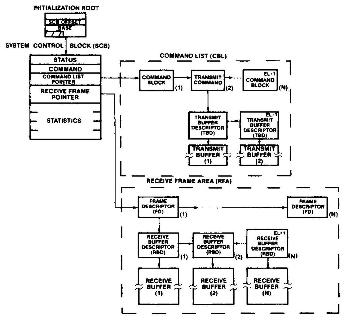
The diagram below shows the data structures in shared memory for communication between the main processor and the coprocessor. The Command List specifies the commands that the coprocessor should perform. The Receive Frame area provides memory blocks for incoming network packets.
A diagram of the 82586 shared memory structures, from the 82586 datasheet.I think Intel was inspired by mainframe-style I/O channels, which moved I/O processing to separate processors communicating through memory. Another sign of Intel's attempts to move mainframe technology to microprocessors was the ill-fated iAPX 432 processor, which Intel called a "micro-mainframe." (I discuss the iAPX 432 as part of this blog post.)
-
An alternative approach to networking is token-ring, where the computers in the network pass a token from machine to machine. Only the machine with the token can send a packet on the network, ensuring collision-free transmission. I looked inside an IBM token-ring chip in this post. ↩
-
Ethernet's technique is called CSMA/CD (Carrier Sense Multiple Access with Collision Detection). The idea of Carrier Sense is that the "carrier" signal on the network indicates that the network is in use. Each computer on the network listens for the lack of carrier before transmitting, which avoids most collisions. However, there is still a small chance of collision. (In particular, the speed of light means that there is a delay on a long network between when one computer starts transmitting and when a second computer can detect this transmission. Thus, both computers can think the network is free while the other computer is transmitting. This factor also imposes a maximum length on an Ethernet network segment: if the network is too long, a computer can finish transmitting a packet before the collision occurs, and it won't detect the collision.) Modern Ethernet has moved from the shared network to a star topology that avoids collisions. ↩
-
The length of the mask is one more than the three-bit length input. E.g. An input of 7 sets eight mask bits. ↩
-
The mask generation logic is a bit tricky to understand. You can try various bit combinations to see how it works. The logic is easier to understand if you apply De Morgan's law to change the NOR gates to AND gates, which also removes the negation on the inputs. ↩
-
The control line appears to enable or disable mask selection but its behavior is inexplicably negated on bit 1. ↩
-
The circuitry below the counter appears to be a state machine that is unrelated to the exponential backoff. From reverse engineering, my hypothesis is that the counter is reused by the state machine: it both generates pseudorandom numbers for exponential backoff and times events when a packet is being received. In particular, it has circuitry to detect when the counter reaches 9, 20, and 48, and takes actions at these values.
The state itself is held in numerous latches. The new state is computed by a PLA (Programmable Logic Array) below and to the right of the counter along with numerous individual gates. ↩
-
One drawback of this exponential backoff circuit is that the pseudorandom numbers are completely synchronous. If two network nodes happen to be in the exact same counter state when they collide, they will go through the same exponential backoff delays, causing a collision every time. While this may seem unlikely, it apparently happened occasionally during use. The LANCE Ethernet chip from AMD used a different approach. Instead of running the pseudorandom counter from the highly accurate quartz clock signal, the counter used an on-chip ring oscillator that was deliberately designed to be inaccurate. This prevented two nodes from locking into inadvertent synchronization. ↩
5 comments:
I wrote and maintained the Intel 82586 "ie" and AMD Lance 7990 "le" ethernet drivers at Sun Microsystems back in the day.
Interesting semi-related story, Sun contracted NCR Fort Collins to reverse-engineer several vendor i/o chips including the AMD Lance to produce a pair of (bug-compatible) integrated ASICs. The project reduced costs and uncovered several interesting long lurking chip bugs.
neal
Out of (morbid) curiosity, did you know anyone who worked on HME? I've hacked a bit on the Linux driver. The comments are littered with David Miller's frustrations with the hardware (as I can attest to).
Hello, very nice article.
how may transistor does this chip contain ?
Ken,
Will you be doing a followup on some other classic chips of that era, like the AMD Lance or the DEC Tulip chips? That would be a great compare/contrast to see how different teams solved the same problem space with different tradeoffs. Those tulip cards were the most reliable back in the day under linux as I recall, Don Becker wrote a bunch of those drivers if I recall correctly.
Neal,
Can you share some more stories as well? And it's interesting about the ASICs, did Sun do this so they could put a single ASIC on the motherboard and not have to use a PCI slot for an ethernet port?
And I too would love to learn more about the hme# design as well.
I'm not sure about the action at counter value 20, but 9 is probably the multicast hash, and 48 is obviously when the destination address has been fully received, both of which are key receiver logic.
Post a Comment