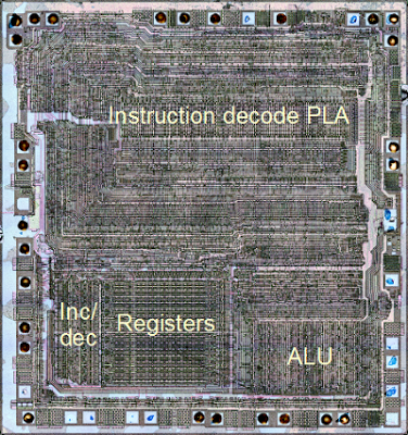
The image above shows the overall organization of the Z-80 chip. I'm going to zoom way in on the ALU and look at the silicon that implements one of the complex gates there: a 5-input, three-level gate. I'll walk through this gate and show how it works at the silicon level. While the silicon look like a jumble of lines, its operation is actually straightforward if you step through it.
Let's begin with an (oversimplified) description of how the chip is constructed. The chip starts with the silicon wafer. Regions are diffused with an element such as boron, yielding conductive diffusion regions. A layer of polysilicon strips is put on top. Finally, a layer of metal "wires" above the polysilicon provides more connections. For our purposes, diffusion regions, polysilicon, and metal can all be consider conductors.
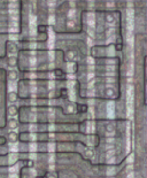
In the image below, the bright vertical bands are metal wires. The slightly darker horizontal bands are polysilicon; the borders are more visible than the regions themselves. In this part of the Z-80, the polysilicon connections run mostly horizontally, and the metal wires run vertically. The large irregular regions outlined in black are doped silicon diffusion regions. The circles are vias between different layers.
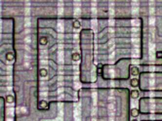
Transistors are formed where a polysilicon line crosses a diffusion region. You might expect transistors to be very visible in the image, but a polysilicon line looks the same whether its a conductor or a transistor. So transistors just appear as long skinny regions in the image. The diagram below shows the physical structure of a transistor: the source and drain are connected if the gate is positive.

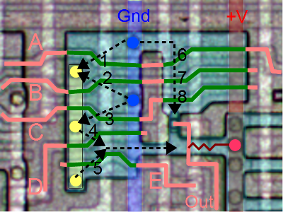
With all the pieces labeled, we can figure out the operation of the circuit. If input A is high, the first transistor will conduct and connect the yellow strip to ground (dotted line 1). Likewise, if input B is high, the second transistor will conduct and ground the yellow strip (dotted line 2). C will ground the yellow strip via 3. So the yellow strip will be grounded for A or B or C. This forms a three-input OR gate.
If input D is high, transistor 4 will connect the yellow strip to the output. Likewise, if input E is high, transistor 5 will connect the yellow strip to the output. Thus, the output will be grounded if (A or B or C) and (D or E).
In the upper right, arrow 6/7/8 will ground the output if A and B and C are high and the three associated transistors (6, 7, 8) conduct. This computes A and B and C.
Putting this all together, the output will be grounded if [(A or B or C) and (D or E)] or [A and B and C]. If the output is not grounded, the resistor (actually a depletion transistor) will pull the output high. Thus, the final output is not [(A or B or C) and (D or E)] or [A and B and C].
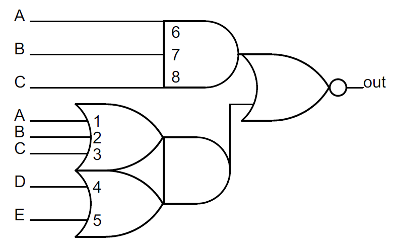
The diagram below shows the gate logic implemented by this circuit. This rather complex gate is created from just nine transistors. Note that the final AND and NOR gates are "for free" - they are formed by wiring together previous outputs and don't require additional transistors. Another point of interest is that with NMOS, the output will be high unless something pulls it low, which explains why circuits are based on NAND and NOR gates rather than AND and OR gates.
If you want to see more low-level silicon analysis, see my article on the overflow circuit in the 6502 at the silicon level.
What does this gate do?
This gate is a key part of one bit of the Z-80's ALU. The gate generates the (inverted) sum, AND, OR, or XOR of B and C depending on the inputs. Specifically, B and C are the two operand inputs, and A is the carry in. D is a control input and E is an inverted intermediate carry from B plus C plus carry_in. By controlling D and overriding A and E, the operation is selected.The Z-80's interesting XOR gate
The Z-80 uses an unusual circuit for its XOR gate. XOR is an inconvenient function to implement since it has a worst-case Karnaugh map, making it expensive to implement from simple gates. Instead, the Z-80 uses a combination of inverters and pass transistors, different from regular NMOS logic.
As before, the diagram below shows the power and ground metal lines, a connecting metal line in yellow, the polysilicon in pink, the polysilicon transistor gates in green, and diffusion in cyan. The two inputs are A and B.
Starting with input A: if it is high, transistor 1 will connect A' to ground. Otherwise the pullup resistor (way on the left), will pull A' high. (Note that A' is the whole diffusion region between transistor 1 and transistor 3 up to the resistor.) Thus transistor 1 forms a simple inverter with inverted output A'. Likewise, transistor 2 inverts input B to give inverted B' (in the whole diffusion region between transistors 2 and 4).
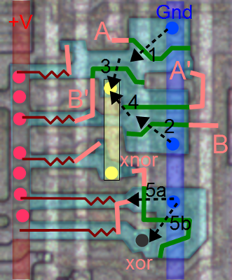
Now comes the tricky part. If A' is high, pass transistor 4 will connect B' to the yellow metal. If B' is high, pass transistor 3 will connect A' to the yellow metal. The third pullup resistor will pull the yellow metal high unless something ties it to ground . Working through the combinations, if A' and B' are both high, both A' and B' are connected to the yellow metal, which gets pulled high. If A' is high and B' is low, B' is connected to the yellow metal, pulling it low. Likewise, if A' is low and B' is high, A' pulls the yellow metal low. Finally if A' and B' are low, nothing gets connected to the yellow metal, so the resistor pulls it high.
To summarize, the yellow metal is pulled high if A' and B' are both high or both low. That is, it is the exclusive-nor of A' and B', which is also the exclusive-or of A and B.
Finally, the xnor value controls transistors 5a and 5b which form an inverter. If xnor is high, transistors 5a and 5b conduct and the xor output is connected to ground, and if xnor is low, the pullup resistors pull the xor output high. One unusual feature here is the parallel transistors 5a and 5b with separate pullup resistors. I haven't seen this in the 8085 or 6502; they use a single larger transistor instead of parallel transistors.
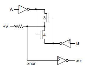
The schematic below summarizes the circuit. In case you're wondering, this XOR gate is used to compute the parity flag. All the bits are XORed together to generate the parity flag.
Comparison to other processors
From what I've seen so far, the Z-80 uses considerably more complex gates than the 8085 and the 6502. The 6502 uses mostly simple NAND/NOR gates and only a few two-level gates, not as complex as on the Z-80. The 8085 uses more complex gates, but still less than the Z-80. I don't know if the difference is due to technical limits on the number of gate levels, or the preferences of the designers.The XOR circuit in the Z-80 is different from the 8085 and 6502. I'm not sure it saves any transistors, but it is unusual. I've seen other pass-transistor implementations of XOR, but none like the Z-80.
Credits: The Visual 6502 team especially Chris Smith, Ed Spittles, Pavel Zima, Phil Mainwaring, and Julien Oster.
4 comments:
Many thanks for your blogs on the Z-80! I am building a Z-80 replica from discrete transistors (surface mount) in CMOS and this project will be a huge help--especially your test cases.
On the XOR circuit: I built an LT-Spice model of it, and it is pretty sensitive to process and resistance value. The problem is that transistors are either turned on conducting ground or they are high resistance, and the base of following transistor has enough capacitance to be a real effect when you are trying to run at a few MHz. The XNOR output has good, sharp transitions to ground, but charging the RC network up delays and rounds the edge of the rising edges.
No question why designers later switched to CMOS process, but this circuit, as built, would not work except in NMOS process.
@Daniel Wisehart, just wondering how your Z80 replica made from discreet components is going? I'd be very interested to have a look, having programmed the Z80 in my high-school and subsequent years, and definitely being my favourite 8-bit processor.
This discreet 6502 https://monster6502.com/ caught my eye some time back, but your post here, is the first mention AFAIK of a similar project for the Z80. It'd have a few more transistors (more than double).
Hope you get a chance to finish it!
Yes, I too am curious how your discrete Z80 is coming! The MOnSter 6502 is impressive when you see it in person; but due to lots of issues, speed is limited.
Nonetheless, I would love to see your progress to date on your transistor-level Z80. Thanks!
Yes, I too am curious how your discrete Z80 is coming! The MOnSter 6502 is impressive when you see it in person; but due to lots of issues, speed is limited.
Nonetheless, I would love to see your progress to date on your transistor-level Z80. Thanks!
Post a Comment