
The increment/decrement circuit in the lower left corner of the chip photograph above. This circuit takes up a significant amount of space on the chip, illustrating its complexity. It is located close to the register file, allowing it to access the registers directly.
The fundamental use for an incrementer is to step the program counter from instruction to instruction as the program executes. Since this happens at least once for every instruction, a fast incrementer is critical to the performance of the chip. For this reason, the incrementer/decrementer is positioned close to the address pins (along the left and bottom of the photograph above). A second key use is to decrement the stack pointer as data is pushed to the stack, and increment the stack pointer as data is popped from the stack. (This may seem backwards, but the stack grows downwards so it is decremented as data is pushed to the stack.)
The incrementer/decrementer in the Z-80 is also used for a variety of other instructions. For example, the INC and DEC instructions allow 16-bit register pairs to be incremented and decremented. The Z-80 includes powerful block copy and compare instructions (LDIR, LDDR, CPIR, CPDR) that can process up to 64K bytes with a single instruction. These instructions use the 16-bit BC register pair as a loop counter, and the decrementer updates this register pair to count the iterations.
One of the innovative features of the Z-80 is that it includes a DRAM refresh feature. Because Dynamic RAM (DRAM) stores data in capacitors instead of flip flops, the data will drain away if not accessed and refreshed every few milliseconds. Early microcomputer memory boards required special refresh hardware to periodically step through the address space and refresh memory. The incrementer is used to update the address in the refresh register R on each instruction. (Current systems still require memory refresh, but it is handled by the DDR memory modules and memory controller).
Architecture
The architecture diagram below provides a simplified view of how the incrementer/decrementer works with the rest of the Z-80. The incrementer is closely associated with the 16-bit address bus. The data bus, on the other hand, is only 8 bits wide. Many of the registers are 8 bits, but can be paired together as 16-bit registers (BC, DE, HL).A 16-bit latch feeds into the incrementer. This is needed since if a value were read from the PC, incremented, and written back to the PC at the same time a loop would occur. By latching the value, the read and write are done in separate cycles, avoiding instability. On the chip, the latch is between the incrementer and the register file.
The program counter and refresh register are separated from the rest of the registers and coupled closely to the incrementer. This allows the incrementer to be used in parallel with the rest of the Z-80. In particular, for each instruction fetch, the program counter (PC) is written to the address bus and incremented. Then the refresh address is written to the address bus for the refresh cycle, and the R register is incremented. (Note that the interrupt vector register I is in the same register pair as the R register. This explains why the I value is also written to the address bus during refresh.)

One of the interesting features of the Z-80 is a limited form of pipelining: fetch/execute overlap. Usually, the Z-80 fetches an instruction before the previous instruction has finished executing. The architecture above shows how this is possible. Because the PC and R registers are separated from the other registers, the other registers and ALU can continue to operate during the fetch and refresh steps.
The other registers are not entirely separated from the incrementer/decrementer, though. The stack pointer and other registers can communicate via the bus with the incrementer/decrementer when needed. Pass transistors allow this bus connection to be made as needed.
How a simple incrementer/decrementer works
To understand the circuit, it helps to start with a simple incrementer. If you've studied digital circuits, you've probably seen how two bits can be added with a half-adder, and several half-adders can be chained together to implement a simple multi-bit increment circuit.The circuit below shows a half-adder, which can increment a single bit. The sum of two bits is computed by XOR, and if both bits are 1, there is a carry.

Chaining together 16 of these half-adder circuits creates a 16-bit incrementer. Each carry-out is connected to the carry-in of the next bit. A 1 value is fed into the initial carry-in to start the incrementing.
This circuit can be converted to a decrement circuit by renaming the carry signal as a borrow signal. If a bit is 0 and borrow is 1, then there must be a borrow from the next higher bit. (This is similar to grade-school decimal subtraction: 101000 - 1 = 100999 in decimal, since you keep borrowing until you hit a nonzero digit.) When decrementing, a 0 bit potentially causes a borrow, the opposite of incrementing, where a 1 bit potentially causes a carry.
The incrementer and decrementer can be combined into a single circuit by adding one more gate. When computing the carry/borrow for decrementing, each bit is flipped. This is accomplished by using an XOR gate with the decrement condition as an input. If decrement is 1, the input bit is flipped. To increment, the decrement input is set to 0 and the bit passes through the XOR gate unchanged.

Repeating the above circuit 16 times creates a 16-bit incrementer/decrementer.
Ripple carry: the problem and solutions
While the circuits above are simple, they have a big problem: they are slow. These circuits use what is called "ripple carry", since the carry value ripples through the circuit bit by bit. The consequence is each bit can't be computed until the carry/borrow is available from the previous bit. This propagation delay limits the clock speed of the system, since the final result isn't available until the carry has made it way through the entire circuit. For a 16-bit counter, this delay is significant.Carry skip
The Z-80 uses two techniques to avoid ripple carry and speed up the incrementer. First, it uses a technique called carry-skip to compute the result and carry for two bits at a time, reducing the propagation delay.The circuit diagram below shows how two bits at a time can be computed. Both carry values are computed in parallel, rather than the second carry depending on the first. If both input bits are 1 and there is a carry in, then there is a carry from the left bit. By computing this directly, the propagation delay is reduced.

Due to the MOS gates used in the Z-80, NOR and XNOR gates are more practical than AND and XOR gates, so instead of the carry skip circuit above, the similar circuit below is used in the Z-80. The output bits are inverted, but this is not a problem because many of the Z-80's internal buses are inverted. (The Z-80 uses an interesting pass-transistor XNOR gate, described here. The circuit below performs increment/decrement on two bits, and is repeated six times in the Z-80. To simplify the final schematic, the circuit in the dotted box will simply be shown as a box labeled "2-bit inc/dec".

Carry-lookahead
The second technique used by the Z-80 to avoid the ripple carry delay is carry lookahead, which computes some of the carry values directly from the inputs without waiting on the previous carries. If a sequence of bits is all 1's, there will be a carry from the sequence when it is incremented. Conversely, if there is a 0 anywhere in the sequence, any intermediate carry will be "extinguished". (Similarly, all 0's causes a borrow when decrementing.) By feeding the bits into an AND gate, a sequence of all 1's can be detected, and the carry immediately generated. (The Z-80 uses the inverted bits and a NOR gate, but the idea is the same.)In the Z-80 three lookahead carries are computed. The carry from the lowest 7 bits is computed directly. If these bits are all 1, and there is a carry-in, then there will be a carry out. The second carry lookahead checks bits 7 through 11 in parallel. The third carry lookahead checks bits 12 through 14 in parallel. Thus, the last bit of the result (bit 15) depends on three carry lookahead steps, rather than 15 ripple steps. This reduces the time for the incrementer to complete.
For more information on carry optimization, see this or this discussion of adders.
The Z-80's increment/decrement circuit
The schematic below shows the actual circuit used in the Z-80 to implement the 16-bit incrementer/decrementer, as determined by reverse engineering the silicon. It uses six of the 2-bit inc/dec blocks described earlier in combination with the three carry-lookahead gates.In the top half of the schematic, the seven low-order bits are incremented/decremented using the circuit block discussed above. In parallel, the carry/borrow from these bits is computed by the large NOR gate on the left.
Bits 7 through 11 are computed using the carry lookahead value, allowing them to be computed without waiting on the low-order bits. In parallel, the carry/borrow out of these bits is computed by the large NOR gate in the middle, and used to compute bits 12 through 14. The last carry lookahead value is computed at the left and used to compute bit 15. Note that the number of carry blocks decreases as the number of carry lookahead gates increases. For example, output 6 depends on three inc/dec blocks and no carry lookahead gates, while output 14 depends on one inc/dec block and two carry lookahead gates. If the inc/dec blocks and carry lookahead gates require approximately the same time, then the output bits will be ready at approximately the same time.

The image below shows what the incrementer/decrementer looks like physically, zooming in on the die photograph at the top of the article. The layout on the chip is slightly different from the schematic above. On the chip, the bits are arranged vertically with the low-order bit on top and the high-order bit on the bottom.
The image is a composite: the upper half is from the Z-80 die photograph, while the lower half shows the chip layers as tediously redrawn by the Visual 6502 team for analysis. You can see 8 horizontal "slices" of circuitry from top to bottom, since the bits are processed two at a time. The vertical metal wires are most visible (white in the photograph, blue in the layer drawing). These wires provide power, ground, control signals, and collect the lookahead carry from multiple bits. The polysilicon wires are reddish-orange in the layer diagram, while the diffused silicon is green. Transistors result where the two cross. If you look closely, you can see diagonal orange polysilicon wires about halfway across; these connect the carry-out from one bit to carry-in of the next.

Incrementing the refresh register
The refresh register R and interrupt vector I form a 16-bit pair. The refresh register gets incremented on every memory refresh cycle, but why doesn't the I register get incremented too? This would be a big problem since the value in the I register would get corrupted. The answer is the refresh input into the first carry lookahead gate in the schematic. During a refresh operation, a 1 value is fed into the gate here. This forces the carry to 0, stopping the increment at bit 6, leaving the I register unchanged (along with the top bit of the R register).You might wonder why only 7 bits of the 8-bit refresh register get incremented. The explanation is that dynamic RAM chips store values in a square matrix. For refresh, only the row address needs to be updated, and all memory values in that row will be refreshed at once. When the Z-80 was introduced, 16K memory chips were popular. Since they held 2^14 bits, they had 7 row address bits and 7 column address bits. Thus, a 7 bit refresh value matched their need. Unfortunately, this rapidly became obsolete with the introduction of 64K memory chips that required 8 refresh bits. [Edit: it's a bit more complicated and depends on the specific chips. See the comments.] Some later chips based on the Z-80, such as the NSC800 had an 8-bit refresh to support these chips.
The non-increment feature
One unexpected feature of the Z-80's incrementer is that it can pass the value through unchanged. If the carry-in to the incrementer/decrementer is set to 0, no action will take place. This seems pointless, but it actually useful since it allows a 16-bit value to be latched and then read back unchanged. In effect, this provides a 16-bit temporary register. The Z-80 uses this action for EX (SP), HL, LD SP, HL, and the associated IX and IY versions. For the LD SP, HL, first HL is loaded into the incrementer latch. Then the unincremented value is stored in the SP register.The EX (SP), HL is more complex, but uses the latch in a similar way. First the values at (SP+1) and (SP) are read into the WZ temporary register. Next the HL value is written to memory. Finally, WZ is loaded into the incrementer latch and then stored in HL.
You might wonder why values aren't copied between two registers directly. This is due to the structure of the register cells: they do not have separate load and store lines. Instead when a register is connected to the internal register bus, it will be overwritten if another value is on the bus, and otherwise it can be read. Even a simple register-to-register copy such as LD A,B cannot happen directly, but copy the data via the ALU. Since the Z-80's ALU is 4 bits wide, copying a 16-bit value would take at least 4 cycles and be slow. Thus, copying a 16-bit value via the incrementer latch is faster than using the WZ temporary registers.
One timing consequence of using the incrementer latch for 16-bit register-to-register transfers is that it cannot be overlapped with the instruction fetch. Many Z-80 instructions are pipelined and don't finish until several cycles into the next instruction, since register and ALU operations can take place while the Z-80 is fetching the next instruction from memory. However, the PC uses the incrementer during instruction fetch to advance to the next instruction. Thus, any transfer using the incrementer latch must finish before the next instruction starts.
The 0x0001 detector
Another unexpected feature of the incrementer/decrementer is it has a 16-input gate to test if the input is 0x0001 (not shown on the schematic). Why check for 1 and not zero? This circuit is used for the block transfer and search instructions mentioned earlier (LDIR, LDDR, CPIR, CPDR). These operations repeat a transfer or compare multiple times, decrementing the BC register until it reaches zero. But instead of checking for 0 after the decrement, the Z-80 checks if BC register is 1 before the decrement; this works out the same, but gives the Z-80 more time to detect the end of the loop and wrap up instruction execution.No flags
Unlike the ALU, the incrementer/decrementer doesn't compute parity, negative, carry, or zero values. This is why the 16-bit increment/decrement instructions don't update the status flags.Comparison with the 6502 and 8085
The 6502 has a 16-bit incrementer, but it is part of the program counter circuit. The 6502 only provides an incrementer, not a decrementer, as the PC doesn't need to be decremented. The other registers are 8 bits, so they don't need a 16-bit incrementer, but use the ALU to be incremented or decremented. (See the 6502 architecture diagram.) The 6502's incrementer uses a couple tricks for efficiency. It uses carry lookahead: the carry from the lowest 8 bits is computed in parallel, as is the carry from the next 4 bits. Alternating bits use a slightly different circuit to avoid inverters in the carry path, slightly reducing the propagation delay.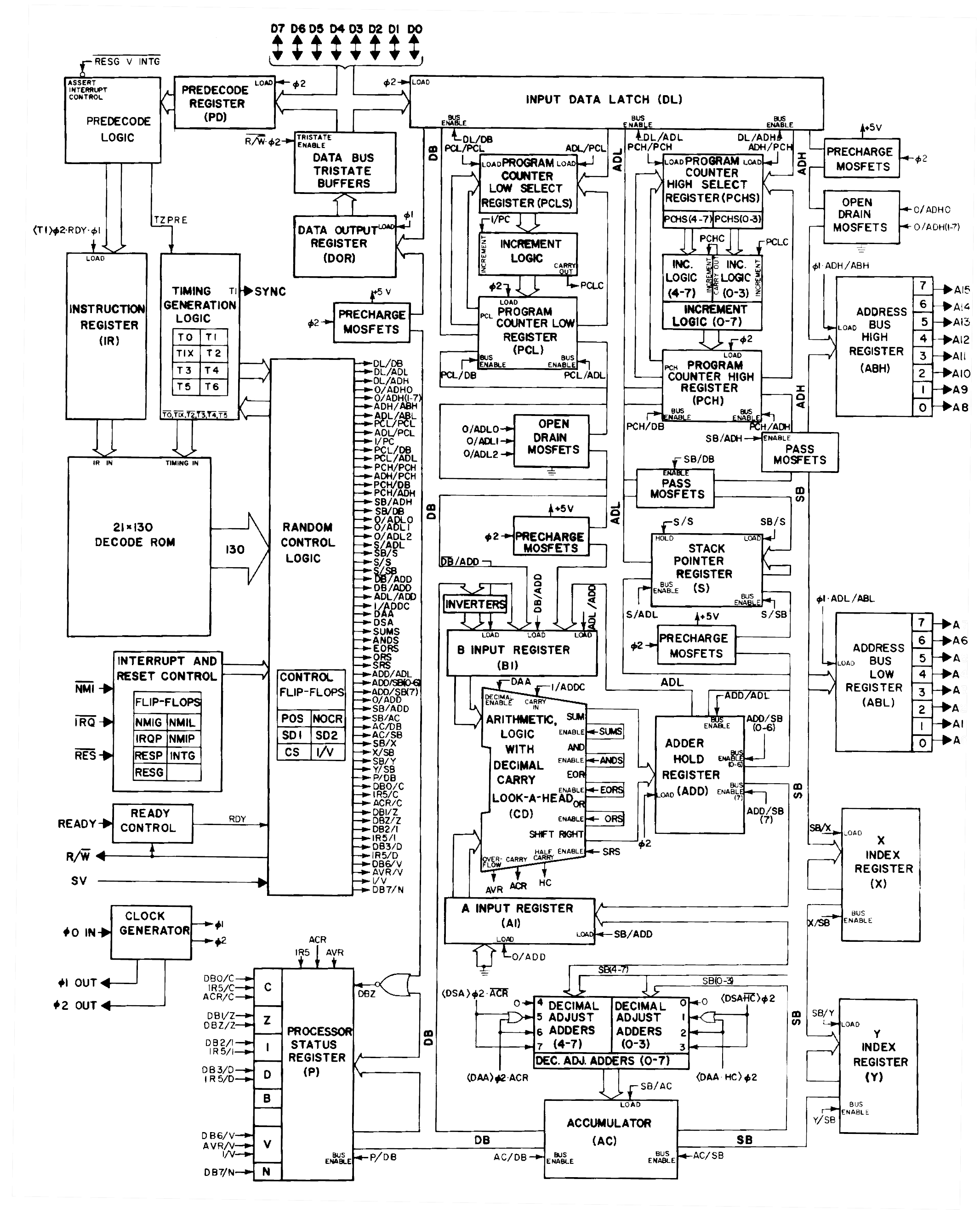
I've examined the 8085's register file and incrementer in detail. The incrementer/decrementer is implemented by a chain of half-adders with ripple carry. The 8085 has controls to select increment or decrement, similar to the Z-80. The 8085 also includes a feature to increment by two, which speeds up conditional jumps. As in the 6502, an optimization in the 8085 is that alternating bits are implemented with different circuits and the carry out of even bits is inverted. This avoids the inverters that would otherwise be needed to flip the carry back to its regular state. The 8085 uses the carry out from the incrementer to compute the undocumented K flag value.
Conclusion
Looking at the actual circuit for the incrementer/decrementer in the Z-80 shows the performance optimizations in a real chip, compared to a simple incrementer. The 6502 and 8085 also optimize this circuit, but in different ways. In addition, examining the circuitry sheds light on how some operations are implemented in the Z-80, as well as the way memory refresh was handled.Credits: This couldn't have been done without the Visual 6502 team especially Pavel Zima, Chris Smith, Ed Spittles, Phil Mainwaring, and Julien Oster.
13 comments:
There is a small error regarding the refresh feature of the Z80.
64KBit-DRAMs (4164) use a 7Bit refresh (128 cycles) despite using 8Bit addresses. This carries through to the 256 KBit DRAMs (41256) which need an 8Bit refresh (256 cycles) despite having 9Bit addresses.
So a Z80 can properly refresh a 64KBit DRAM if the address lines are wired correctly.
Since a 64Kx4 DRAM (41464) is internally 256KBit, it needs an 8Bit refresh.
Apparently it's not quite as simple as Anonymous said above. There's apparently 128-cycle refresh and 256-cycle refresh 4164s. (The first one I found a datasheet for required a full 256 refresh cycles.)
Here's one thread elsewhere that briefly mentions the difference:
http://www.vintage-computer.com/vcforum/showthread.php?36974-4164-DRAM-with-128-refresh
This list from the previous thread shows 128-cycle vs. 256-cycle DRAMs from multiple vendors. http://www.minuszerodegrees.net/memory/4164.htm
Ok, I stand corrected.
All the datasheets of 4164 in my collection state 128 cycle refresh and I never had seen any others.
So in other words, you can refresh 4164 with a Z80 if you wire it right _and_ use the right RAMs.
I'm curious how TMS4532 (partially defective TMS4164) work in a ZX Spectrum though since the upper RAM is refreshed by the Z80 and the TMS4164 are listed as 256 cycle.
Just speculation, but it seems likely that the ZX Spectrum was only refreshing the 128 good rows...
all the z80 reverse engineering stuff on this blog is really cool, I enjoyed reading it. I download the z80 layout and started looking at the register file area.
Any tips on where to start! I guess tracing through the clock, vcc and gnd signals is a good place.
Any idea which pads on the edge of the die are which? How did you start?
Anonymous: if you want to trace the chip, you should get in touch with the Visual 6502 team. But to get you started, ground is the big trace on the left, and +5 is the big trace on the right. The upper-left pin is BUSRQ, upper-right is D1, lower left is A5, and lower-right pin is CLK. You can fill in the rest of the pins by looking at the chip pinout.
Fantastic investigation, Ken! Have you found the adder that should be connected to IX and IY registers to quickly compute (IX+d) addresses? Is that adder somehow part of the incrementer, but not shown? Greetings!
@Anonymous: My own guess is that it uses the 4-bit ALU for that. Compare the cycle time for "LD r, (HL)" to "LD r, (IX+d)". 2M/7T vs. 5M/19T.
If this incrementer was able to do the add, I would expect IX+d to be much faster.
Ken, any thoughts?
Some Z80 block schematics out there actually show the adder but again some don’t. The confusing part is that ALU flags are not affected by it. There must be some signal to inhibit ALU from updating all relevant flags if this was the case.
When you account for 2 extra M cycles (fetching the prefix and “d”), you are left with 1 extra M cycle and 6 T clocks. Those clocks may as well implement this: #1: Xl->ACT, #2: Add, #3: ALU->Z, #4: Xh->ACT, #5:Adc, #6:ALU->W and then next M phase instead of HL->bus, do WZ->bus, so WZ holds the (IX+d). That would add up.
What do you think?
How do I contact someone from the 6502 team to get the Z80 chip traces? I did some investigation of the Z80 instruction register latches here: http://www.devic.us/hacks/z80-instruction-register-deciphered
but having traces would really help me getting further. Ken, how did you get the image of incrementer you compared in this blog? Thanks!
Regarding the faulty DRAM chips and ZX Spectrum refresh, yes, it was in the documentation, that Clive Sinclair, yet again used defective components to build a massively successful product.
He used to do a similar thing with transistors, even pulling them out of the tarmac and recycling. Also, individually (by hand) testing their beta and selling them via ads in the magazines.
Those were the days...
On the 48KB ZX Spectrum, the upper 32KB of memory was wired with physical links to select which half of the TMS4532 chips to use. A7 is wired to a logic 0 for the lower half being good and a logic 1 for the upper half. On early issues, each bank of 16KB had to all be the same type (-20NL3 for low and -20NL4 for high). Later issues of the PCB had links to set each chip separately. If the chips need to be replaced you either have to find an exact match, or swap the links around. Or just use working 4164s! Presumably it was cheaper for Sinclair to obtain and fit 2x 4532 than 1x 4164.
Because A7 is hard-wired, the refresh from the CPU does indeed only touch the working half of the chips. There is no way to access the other half.
Post a Comment