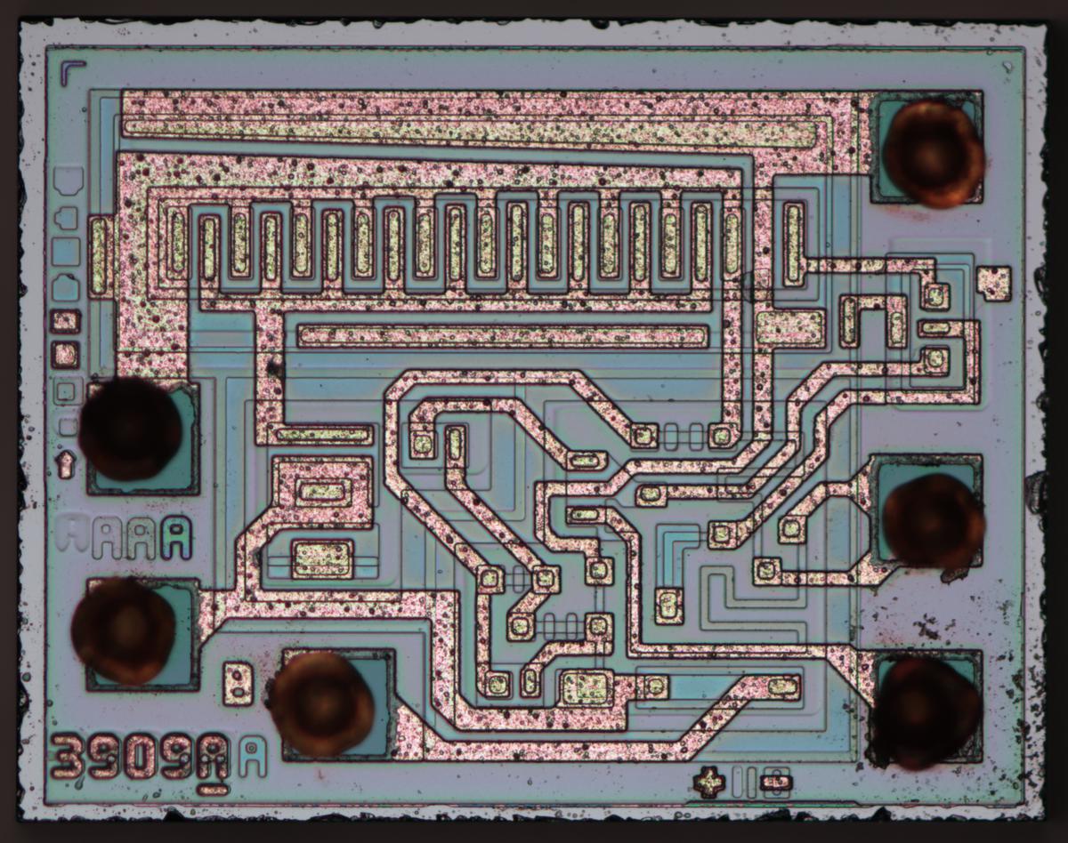
How do you make an LED blink? A vintage way is the LM3909, a chip from 1975 that can flash an LED for a year from a single flashlight battery. This chip has some surprising features, such as a charge pump that lets you power a 2-volt LED from a 1.5-volt battery. This IC was designed for simplicity, using just an LED, external capacitor, and battery. In this blog post, I reverse-engineer its silicon die.
The photo below (from
How it works
The underlying idea of the IC is that the external capacitor slowly charges through the internal timing resistor. When the capacitor reaches about 1 volt, the LED is energized and lights up briefly. This discharges the capacitor and the cycle repeats. Because the LED is only powered in brief pulses, the circuit's power consumption is low, averaging about 550 µA.
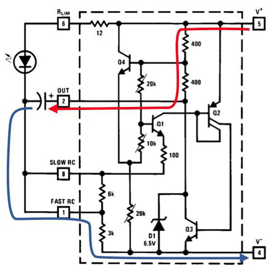
The first phase, charging the capacitor, is shown in the schematic below. The red line indicates how the battery (V+) charges the positive side of the external capacitor (on pin 2) through two 400Ω resistors. The negative side of the capacitor is connected to the negative side of the battery through the 3K resistor. The flashing frequency can be slowed down by disconnecting pin 1. In that case, the capacitor charges through the additional resistance of the "Slow RC" pin.
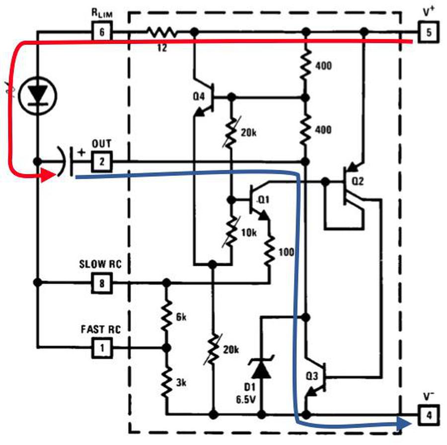
When the capacitor charges to about 1 volt, Q1 turns on, turning on Q2 and then power transistor Q3.1 This causes the circuit to discharge through the LED, as shown below. The tricky part is that the positive side of the capacitor is now connected to ground. Since the capacitor was charged to 1 volt, the negative side of the capacitor is now at -1 volt. (In other words, the capacitor acts as a charge pump.) The result is that the LED sees an extra volt; with a 1.5-volt battery, it receives about 2.5 volts.
The LED receives a high-current pulse for about a millisecond, discharging the capacitor, and then the cycle repeats.
Resistors
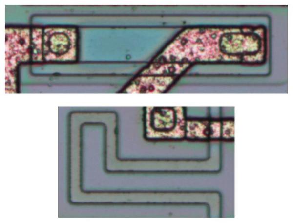
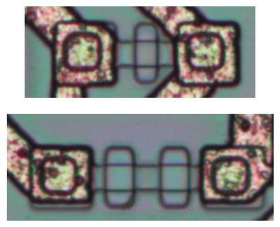
The chip uses numerous resistors. Looking at the die, I'll explain how they are constructed. The first type of resistor uses a strip of doped silicon, which is conductive but has some resistance. The upper resistor in the photo has metal contacts attached to both ends of the resistive rectangle. This resistor is wide and relatively short, so it has a low resistance, 12Ω in this case. (This resistor limits current through the LED, so an external resistor isn't required.) The second resistor is long and narrow, so it has a much higher resistance, 6kΩ. This resistor winds back and forth to fit on the die.
The second type of resistor is a "pinch resistor". An oval of P-type silicon "pinches" the underlying silicon and reduces the current flow. A pinch resistor provides a high resistance in a small space, but is less accurate than the resistors shown earlier. The two resistors below are 10kΩ and 20kΩ respectively.
Transistors
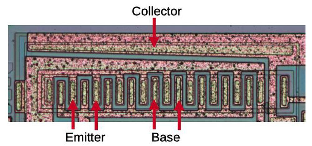
The illustration below shows the power transistor. Since the full current to drive the LED (45 mA) passes through this transistor, it must be relatively large. The metal on top is connected to the collector (N-type silicon). The base (P) and emitter (N) are interdigitated, allowing high current flow. Note that the collector metal gets wider from left to right, while the emitter metal gets narrower. This design puts the widest metal where the current is highest; on the right, the emitter metal carries current from just one emitter "finger", while on the left the metal carries the full emitter current.
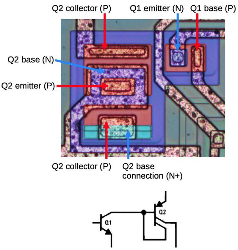
Two other transistors, Q1 and Q2, have an optimized layout where they are partially merged together. I'll try to explain them in the diagram below, but it's a bit tricky. I've colored the die photo to indicate P-type silicon in red and N-type silicon in blue. I'll start with Q2, a transistor with two collectors. (It may seem strange to have two collectors on a transistor, but this is common in analog integrated circuits.) Since Q2 is a PNP transistor, the emitter is P-type silicon, the base is N, and the collectors are P. Q2's emitter (P) is the small rectangle indicated in red; the silicon is connected to the metal on top. Q2's base is formed by a ring of N-type silicon around the emitter. This N-type silicon forms the large blue region over most of the diagram. Finally, Q2's two collectors are the red regions above and below the emitter. (The layers of P, N, and P silicon for the emitter, base, and collector form the layers of the PNP transistor.)k The upper collector is connected to the metal wiring. The lower collector is connected to the base by the lower metal contact.
Now for Q1, an NPN transistor. It has a small square emitter (N, blue) connected to metal wiring. The emitter is embedded in the base region (red, P) that surrounds it. Metal wiring is connected to Q1's base. Q1's collector isn't explicitly visible; the underlying blue region that surrounds the base forms the collector. Note that this blue region also formed Q2's base. Thus Q1's collector and Q2's base are formed by the same large region of N-type silicon, implicitly wiring them together. Analog integrated circuits often optimize the layout of transistors, but this layout is trickier than most.
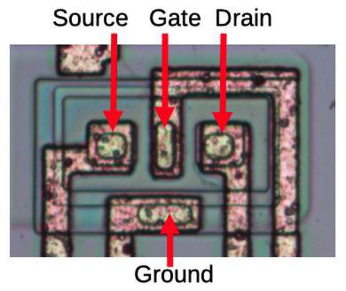
There's one transistor that appears on the die but not on the schematic. It is a JFET (junction field-effect transistor). JFETs are often used on integrated circuits as a compact way to provide a small current. This JFET pulls the base of the power transistor low, probably to ensure that the chip starts up correctly.
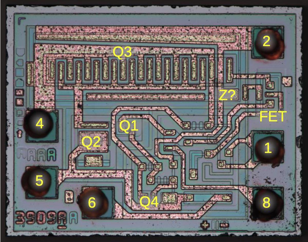
Putting this all together, the diagram below labels the main components on the die. This can be compared with the schematic.2
Conclusion
This integrated circuit has just a few, large components, so their wiring can be traced out on the die.3 The designers came up with a clever circuit that uses just a few transistors but can flash an LED without consuming much power. One interesting feature is the use of a charge pump, so a single 1.5V battery can light an LED that requires more than 1.5V. Another nice feature is that the current-limiting resistor and the timing resistors are part of the IC, so external resistors are not required. On-chip capacitors are very limited, so the chip requires an external capacitor, though.4 Nowadays, you can get an LED with blinking built in, so a special-purpose chip is unnecessary.
Thanks to Zeptobars for the die image and thanks to Jerry Taylor for suggesting this chip. I announce my latest blog posts on Twitter, so follow me @kenshirriff. I also have an RSS feed.
Notes and references
-
I'll use this footnote to explain some details of the circuit. The voltage level on the capacitor is detected by Q1. A transistor turns on when the base voltage is about 0.7 volts above the emitter voltage. A typical transistor circuit modifies the base voltage. But in this case, the base voltage is fixed and the emitter voltage varies. Specifically, Q1's emitter is connected to the capacitor's low side through the 100Ω resistor, so as the capacitor charges, the emitter voltage drops.
When Q1 turns on, current flows through Q1 from Q2. Transistor Q2 has two collectors and is wired as a current mirror: the current through the first collector is copied, creating a current through the second collector. (From the datasheet, Q3 is constructed so the output current is multiplied by 3. This is accomplished by making the upper collector three times larger; you can see on the die that it wraps around three sides of the emitter while the "input" collector is smaller, only on the bottom side.) This current flows into the base of Q3, the power transistor, turning it on. Q4 provides negative feedback to keep Q1 biased correctly. ↩
-
I think the Zener diode is in the location marked "Z", but I'm not sure since there's not a lot to see on the die for a Zener diode. The diode protects the output transistor against excessive voltage. ↩
-
For more information, see the datasheet and Application Note. The application note gives many circuits that use this chip, including unexpected possibilities such as building a radio out of it, or a logic gate. (I think the designers got a bit carried away.) ↩
-
An interesting project is the re-creation of the LM3909 from discrete components by Dillon Nichols; see the writeup and video. (I had no idea that this chip was popular enough that someone would build a clone.) ↩
12 comments:
Today you can buy LEDs with the blink circuitry built into the LED. You don't get to choose the blink rate though.
Dear Ken,
Thanks for doing this "simple" chip. It really helps us non-experts understand the process of building a chip and designing it so much better than taking on something full scale like the 8050!
It is fascinating to see how the components were laid out, and how each part was formed in VLSI. Would love to see a breakdown of the super common 555 timer chip and/or the 741 op-amp just to understand how analog devices are constructed in silicon!
Thanks for your entertaining and educational content. Your efforts are very much appreciated.
Shaunak De: you're in luck! I discussed the 741 here and the 555 here.
The sole mention of the LM3909 on Wikipedia ...Pulse (Pink Floyd lbum) LED_packaging
Early CD versions came with a flashing red LED on the side of the case. This was designed by EMI contractor Jon Kempner, who was awarded the platinum disc, using the now discontinued LM3909 LED flasher IC.
Actually, Russel, 5mm Red LEDs with an embedded flasher chip were available around the time the LM3909 was widely available. I have a few somewhere. The actual chip used was never disclosed, although it was very likely the LM3909. You could clearly see the die as a little black dot on the lead mounting frame.
The flashing leds available don’t do the voltage boost, don’t require the large external cap (typically 300uF), and don’t have the tiny power consumption.
As I recall, the LED's with the built-in chip that I used to get from Radio Shack in the late 70's were not a milisecond blink like the 3909 but had a substantial "on" time and thus a far shorter battery life. I believe they also needed at least 3 volts to work. The 3909 can go over 2 years one "D" cell.
Thanks for the shoutout on my disintegrated LM3909 project. It was inspired by EMSL's “Three Fives” discrete 555 timer kit. I don't know of many other application ICs that can easily be recreated discreetly. Do you have any ideas that aren't just a logic chip?
Hi Ken, thanks for the post.
I wonder about the role of transistor Q4, like you said, Q4 provides negative feedback, namely, if the capacitor voltage increase, the base voltage of Q4 increases too, increasing its collector current and hence, the base voltage of Q1 decreases due to the drop voltage in the 20k resistor. If I'm right, this is done to steady the system? I mean, to give time to discharge the capacitor enough until the transistor Q1 doesn't drive again.
Thank you again.
Unknown: I don't have an intuitive way to explain Q4, but you can take a look at the Application Note and see how they explain it.
Dillon: I can't think of other popular yet simple ICs that would be good to re-create discretely. A 7805 voltage regulator? Maybe too boring.
Is there any schematic for rgb flashing led.
In note 1, second paragraph, inside the parentheses, you said Q3 but after the parentheses you say it goes to Q3. Is the one inside the parentheses Q2? Thanks for the very interesting blog. I have never been able to find a menu or table of contents for your blog. Might be because I've been linking to it from within Facebook.
Post a Comment