The Arduino language lets you program microcontrollers at a high level, controlling I/O pins without worry about exactly
how the microcontroller works.
But what's really going on behind the scenes?
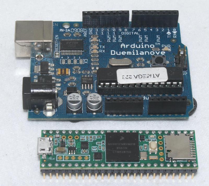
For my current project, I'm using a Teensy 3.6,1
a development board packaged in a breadboard-compatible 48-pin module that is
considerably smaller than a classic Arduino.2
The Teensy uses a fairly powerful microcontroller, a 32-bit ARM processor running at 180 megahertz, and it is (mostly) compatible with
the Arduino programming environment.
I wanted to understand the low-level hardware better, so I investigated the implementation of one of the Arduino functions.
Specifically, this post explains exactly how the analogWrite() function works in the Teensy 3.6.
Disclaimer: this blog post goes into excessive detail on an obscure subject, so feel free to stop reading now :-)
analogWrite(): creating a PWM output
The Arduino IDE lets you quickly create an application using functions that abstract away the microcontroller's implementation details. In comparison, if you program a microcontroller directly, its hardware functions are activated by accessing special memory locations that act as control registers. There may be thousands of registers, different for each microcontroller, and described in thousand-page manuals, so programming a microcontroller directly can be daunting.
Using the Arduino library, you can put a voltage on an output pin with
the analogWrite(pin, value) function. You specify a value between 0 and 256, where 0 is completely off and 256 is completely
on and the library takes care of the details.
For instance, analogWrite(pin, 64) produces an output value of 25% (i.e. 64/256).
You might expect this would produce an analog voltage at 25% of the maximum, but
despite the function's name, the output is not analog. Instead it is a digital pulse-width modulated (PWM) signal, which averages out to the desired value.3
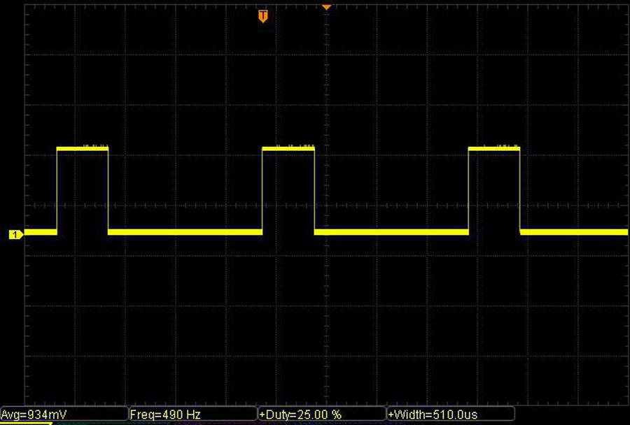
As the oscilloscope trace below shows, the output switches between full-on and full-off, remaining on 25% of the time.4
Even though it doesn't produce a true analog output, the analogWrite function is useful for many tasks, such as controlling LED brightness.
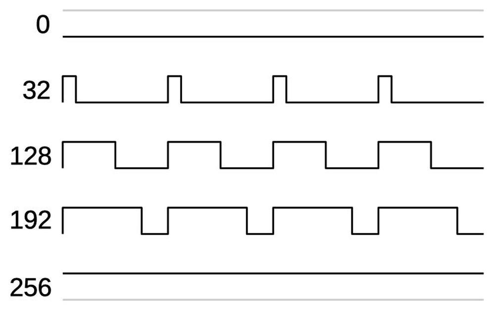
The diagram below shows how the output changes with different analogWrite values, from 0 (completely off) to 256 (completely on).
The main point is that the output is really digital, with a larger input parameter causing the output to be on for a larger fraction of the time.
This technique is called Pulse Width Modulation (PWM), since the width of the pulse changes with the input.
The diagram below illustrates how the microcontroller produces the PWM output. Internally, a timer repeatedly counts from 0 to 255, generating a counter value. Each time the timer starts at 0, the output is set high. When the timer matches the specified value (64 in this case), the output goes low. Thus, the match value controls how long the output remains high in each cycle; the larger the value, the longer the output remains high. The timer increments every 8 microseconds, so the total cycle length is 2048 microseconds, yielding a frequency of 490 Hz.
The analogWrite function is sufficient for most purposes, but how does it work at the microcontroller register level?
The manual for the Teensy's MK66FX1M0 processor explains how the chip's registers work, but is 2237 pages long.
(I've extracted the relevant bits and give references to manual sections if you want to know more.)
The code for the Teensy implementation of analogWrite is in a file called pins_teensy.c.
Because the code supports multiple processors, it is full of #ifdefs;
the Teensy 3.6 code is selected by the __MK66FX1M0__ and KINETISK5 defines, specifying the processor type and family.
The code contains a bunch of case statements to handle all the different types of PWM pins.
I'm using pin 30 in my example, which is defined
in that file as FTM2_CH1_PIN (FlexTimer 2 Channel 1 pin). (I'll explain below why this timer is pin 30.)
The code to handle that pin is:
cval = ((uint32_t)val * (uint32_t)(FTM2_MOD + 1)) >> analog_write_res;
FTM2_C1V = cval;
FTM_PINCFG(FTM2_CH1_PIN) = PORT_PCR_MUX(3) | PORT_PCR_DSE | PORT_PCR_SRE;
As you can see, this code is much more complex than the analogWrite() call.
In brief, the first line computes the counter value (match value) at which the output should go to 0.
The second line stores this value into the timer control register.
The third line configures pin 30 for the timer output.
Next, I'll explain each of these lines in more detail.
The first line handles the difference between the conceptual timer (counting from 0 to 255) and the physical implementation of the timer,
which is 16 bits and counts at a much higher rate.
To match the Arduino's PWM frequency (490 Hz), the Teensy timer counts to 61439.
This line scales the input value (0 to 256) to the desired range (0 to 61440).
Specifically, the hardware register FTM2_MOD (timer 2 modulo) holds 61439, the value that this timer counts to.6
Multiplying the input value by 61440 and dividing by 256 scales the input value to the new range.
(The value 8 for analog_write_res indicates 8 bits of count resolution, i.e. 256.)7
The next line of code stores this value into timer 2's Channel 1 Value register FTM_C1V,8 which controls the pulse width.
This register holds the "match value"; when the timer counter reaches this value, the output drop to 0.
The third line configures pin 30 for the output from the timer.
The FTM_PINCFG macro handles pin configuration, which in this case updates the configuration for pin 30 (CORE_PIN30_CONFIG).11
The PORT_PCR_MUX(3) macro selects the pin's function from the pin multiplexer, which I'll explain in the next section.10
The PORT_PCR_DSE option sets Drive Strength Enable, enabling high-current output.
The PORT_PCR_SRE option sets Slew Rate Enable, slowing the pin's slew rate (how fast it changes value).9
These values are combined and stored in the appropriate bit fields of the Pin Control Register, shown below.
(The macros ensure that each value goes into the right position.)
Filling in the macros, the original analogWrite(30, 64) call becomes:
*(uint32_t *)0x400B8018 = 15360;
*(uint32_t *)0x4004A04C = 0x344;
Thus, in the end, the analogWrite call turns into two stores to microcontroller registers.
Determining the pin and its function
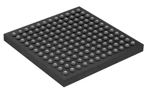
Pin configuration is more complex than you might expect. The problem is that the processor chip has 144 pins (in a 12×12 grid), but the microcontroller provides a much larger number of functions. The solution is that each pin has up to 8 different multiplexed functions, and you can select one of these functions for each pin. Thus, you can't use all the features of the chip at the same time, but hopefully you can use the features you need.
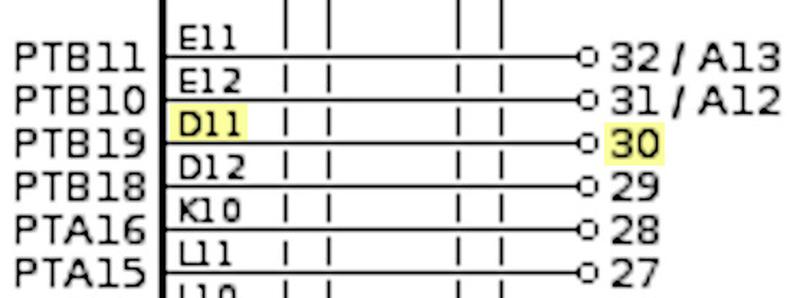
In the example I'm using GPIO pin 30, but this pin number is part of the Arduino API: the microcontroller has no pin 30. So how does pin 30 get a meaning? In this section, I explain how pin 30 maps onto a physical pin of the microcontroller (pin D11 in this case) associated with a PWM timer (FlexTimer 2 channel 1 in this case).
The function of each Teensy pin is documented, but I wanted to figure out "from scratch" what GPIO pin 30 means. Looking at the schematic shows the Teensy's pin 30 is connected to pin D11 of the processor, which is labeled "PTB19". (Processor pins are labeled with a letter and number corresponding to the pin's grid position.)
Chapter 11 of the manual lists the names and functions for each pin (excerpted below). As mentioned earlier, each physical pin supports multiple functions. Pin D11 has the official name "PTB19" and has seven different functions assigned to it: Touch Screen, GPIO PorT B, CAN bus, FlexTiMer FTM2_CH1 (that we're using), I2S audio, FlexBus, and FlexTiMer 2 Quadrature Decoder.
Each pin has a multiplexer (MUX) that selects which function is assigned to the pin.
In order to use the timer with pin D11, the pin configuration register (PCR) for D11 must be configured to assign function 3 to this pin.
This was done with the macro discussed earlier, PORT_PCR_MUX(3).
Thus, when an analogWrite is performed, the pin is configured to use the appropriate timer.
Initialization
Another piece necessary to make this work is the Teensy's initialization code.
The main routine in main.cpp
calls _init_Teensyduino_internal_(), which performs the necessary register initialization.
The timer 2 initialization code is
FTM2_CNT = 0;
FTM2_MOD = DEFAULT_FTM_MOD;
FTM2_C0SC = 0x28;
FTM2_C1SC = 0x28;
FTM2_SC = FTM_SC_CLKS(1) | FTM_SC_PS(DEFAULT_FTM_PRESCALE);
This sets the initial counter value to 0 and sets the modulo value (maximum count) to 61439 as discussed earlier.
The FTM2_C0SC and FTM2_C1SC lines enable PWM mode. The FTM2_SC line sets up the timer clock.12
The last piece is how the code knows the processor type.
To support multiple processor types, the files are full of #ifdefs, but where do these get defined?
The answer is that the board type and CPU speed are set in the Arduino IDE. The IDE uses these settings to generate flags that are passed to the compiler when compiling the code.
The relevant lines for the Teensy 3.6 are in the file hardware/teensy/avr/boards.txt:
teensy36.build.flags.defs=-D__MK66FX1M0__ -DTEENSYDUINO=153
teensy36.menu.speed.180.build.fcpu=180000000
Conclusion
At this point we've reached the foundation. To summarize, the board that you select in the Arduino IDE causes various flags to be passed to the C++ compiler.
These flags, in turn, select numerous definitions of registers for that processor, along with the appropriate code.
The result is that a function call such as analogWrite(30), acting on an abstract pin 30, gets converted to operations on special microcontroller registers,
causing the microcontroller's circuitry to output the desired signal.
It may seem like magic that high-level operations end up doing the right thing across a wide range of microcontrollers, but this is one of the key accomplishments of the Arduino ecosystem. If you really need to know what's going on, I've shown how these abstractions can be unwrapped. But for the most part, the complexity underneath can fortunately be ignored.
I announce my latest blog posts on Twitter, so follow me @kenshirriff. I also have an RSS feed. I wrote about Arduino PWM and its registers in detail here if you want to know more about PWM. Thanks to Paul Stoffregen for answering my questions about Teensy.
Notes and references
-
Why am I using a Teensy 3.6 instead of a newer model? Because the more recent Teensy 4.1 was out of stock. ↩
-
There are also Arduino models in the DIP form factor, such as the Arduino Nano and Arduino Micro. Arduino also has high-power models such as the 32-bit ARM-based Arduino Portenta. ↩
-
The Teensy 3.6 has two digital-to-analog converter (DAC) outputs. For those two pins, the
analogWrite()function produces a genuine analog voltage, not a PWM output. ↩ -
The PWM output has a period of 2048 µs, yielding a frequency of about 490 Hertz. The output is controlled in units of 8 µs, so an input value of 1 yields a pulse width of 8 µs, an input of 64 yields a pulse width of 512 µs and so forth. ↩
-
I tried to sort out what "Kinetis" means. NXP has many different microcontrollers and Kinetis is their family of 32-bit mixed-signal ARM Cortex microcontrollers, introduced in 2010. The Kinetis family includes the high-performance K series and the low-power L series. The Teensy 3.x boards use the Kinetis K series and have the preprocessor variable KINETISK defined, while the Teensy LC board uses a Kinetis L processor and has KINETISL defined. ↩
-
The variable FTM2_MOD is defined as the address (400B8008) of the FTM2 modulo register in kinetis.h. Why is the modulo set to 61439? The goal is to make the PWM period match the Arduino's 2048 µs period (approximately 490 Hertz). To see how this happens, start with the Teensy's clock frequency (F_CPU) of 180 MHz. kinetis.h sets the bus frequency
F_BUSto 60 MHz based on this. Then pins_teensy.c uses this for the timer frequencyF_TIMER. For a frequency of 60 MHz, pins_teensy.c setsDEFAULT_FTM_MODto 61439 andDEFAULT_FTM_PRESCALEto 1. This prescale value causes the timer to divide its input frequency by 2, so the timer runs at 30 megahertz. At this frequency, 61440 ticks will take 2048 µs as desired.Figuring out the address for
FTM_MOD2is more confusing than I expected. If you look at the memory map in the manual (Section 45.4.2), the address for FTM2_MOD is 4003A008 (Peripheral bridge 0), but the Teensy uses address 400B8008 (Peripheral bridge 1, Table 5-3), see kinetis.h. It turns out that the chip has two paths for accessing peripherals: AIPS0 and AIPS1. The timer can be accessed through both paths, but with different register addresses.Another confusing thing is that if you try to access FTM2_MOD through the first address, the Teensy will crash. The reason is that the microcontroller lets you conserver power by turning off the clock to each module, a function called "clock gating". If you try to access a peripheral when the clock is disabled, the system terminates with an error. The two different paths to the timer are controlled by separate clocks. Specifically, access through AIPS0 is enabled through System Clock Gating Control Register 6 (SIM_SCGC6, section 13.2.16), while access through AIPS1 is enabled through SIM_SCGC3 (sections 13.2.13). The Teensy startup code enables timer FTM2 through clock gating register SIM_SCGC3 (for AIPS1) but not SIM_SCGC6 (for AIPS0). Thus, accessing the timer through AIPS1 works, but accessing it through AIPS0 crashes. This thread has more information. ↩
-
By default, the value to
analogWrite()can range from 0 to 256, i.e. 8 bits of resolution. However, the resolution can be changed by callinganalogWriteResolution. Higher resolution gives finer-grain control over the PWM width.The Teensy extensions to Arduino include a function
analogWriteFrequency(), which provides a more convenient way of modifying the PWM frequency. ↩ -
The Register Descriptions section (45.4.2) describes the memory address for each register.
FTM2_C1Vis the "Channel Value" at address 4003A018. Section 45.4.7 explains that this register holds the 16-bit counter value that the timer matches against. ↩ -
On my breadboard, a signal has a rise time of 7.5 nanoseconds with slew rate disabled and 15 nanoseconds with slew rate enabled. The fast signal has a bunch of ringing, while the slower signal rises smoothly. ↩
-
The Pin Control Register is described in section 12.5.1 with details in chapter 11, Signal Multiplexing and Signal Descriptions. ↩
-
The macro
FTM_PINCFG(FTM2_CH1_PIN)turns intoCORE_PIN30_CONFIG, the appropriate configuration register. This is defined in core_pins.h asPORTB_PCR19. The manual (section 12.5) specifies thatPORTB_PCR19(Port B Pin Control Register 19) has address 4004A04C. ↩ -
Register constants
FTM2_C0SCandFTM2_C1SCare set to 0x400B800C and 0x400B8014 respectively in kinetis.h. The manual defines these addresses (section 45.4.2) as 4003_A00C and 4003_A014. (The differences are because the timer can be accessed through a different path (Peripheral Bridge 1) at address 400B_8xxx.) These registers are Channel 0/1 Status and Control, discussed in manual section 45.4.6. Each register has 7 bit fields that control the timer function. The initialization value 0x28 selects Edge-Aligned PWM with high-true pulses.Register constant
FTM2_SC(timer 2 Status and Control) has address 400B8000 in the code and 4003A000 in the manual. Its fields are described in manual section 45.4.3.FTM_SC_CLKS(1)sets theCLKSfield to use the system clock as the timer input.FTM_SC_PSsets the prescale to divide the clock by 2, as discussed earlier. ↩



4 comments:
Great article as always!
I believe that the input range for the `value` parameter to `AnalogWrite()` is 0-255 rather than 0-256.
The Arduino API documentation supports this...
```
value: the duty cycle: between 0 (always off) and 255 (always on). Allowed data types: int.
```
Also, looking at source code for the canonical implementation (the one used by the original AVR-based Arduino boards), we see that passing a 255 as value turns the pin on completely...
```
if (val == 0)
{
digitalWrite(pin, LOW);
}
else if (val == 255)
{
digitalWrite(pin, HIGH);
}
else
{
switch(digitalPinToTimer(pin))
[....PWM code here....]
```
I'll try to find a TEENSY to test with, but my guess is that `analogWrite` with a value of `255` will result in a 100% duty cycle (no PWM) waveform.
Thanks again!
-josh
The teensy 4 is a beast man, can toggle a pin @150MHz via software/bit banging, proven:
#define PIN 13
void setup () { pinMode(PIN, OUTPUT); }
void loop () {
while (1) {
CORE_PIN13_PORTSET = CORE_PIN13_BITMASK;
CORE_PIN13_PORTCLEAR = CORE_PIN13_BITMASK;
}
}
josh: I verified that Teensy turns the pin on completely for an analogWrite value of 256; with a value of 255, it is on 255/256 of the time. While the Arduino divides the PWM cycle into 255 intervals of 8 microseconds, the Teensy has 256 intervals of 8 microseconds, so it goes one higher.
DO I understand this fully, no, will this be helpful for my rocket club to control an EDF, also probably no, was it cool, ooooohhhhh yeaaaaaaa.
Post a Comment