A key component of any processor is instruction decoding: analyzing a numeric opcode and figuring out what actions need to be taken. The Intel 8086 processor (1978) has a complex instruction set, making instruction decoding a challenge. The first step in decoding an 8086 instruction is something called the Group Decode ROM, which categorizes instructions into about 35 types that control how the instruction is decoded and executed. For instance, the Group Decode ROM determines if an instruction is executed in hardware or in microcode. It also indicates how the instruction is structured: if the instruction has a bit specifying a byte or word operation, if the instruction has a byte that specifies the addressing mode, and so forth.
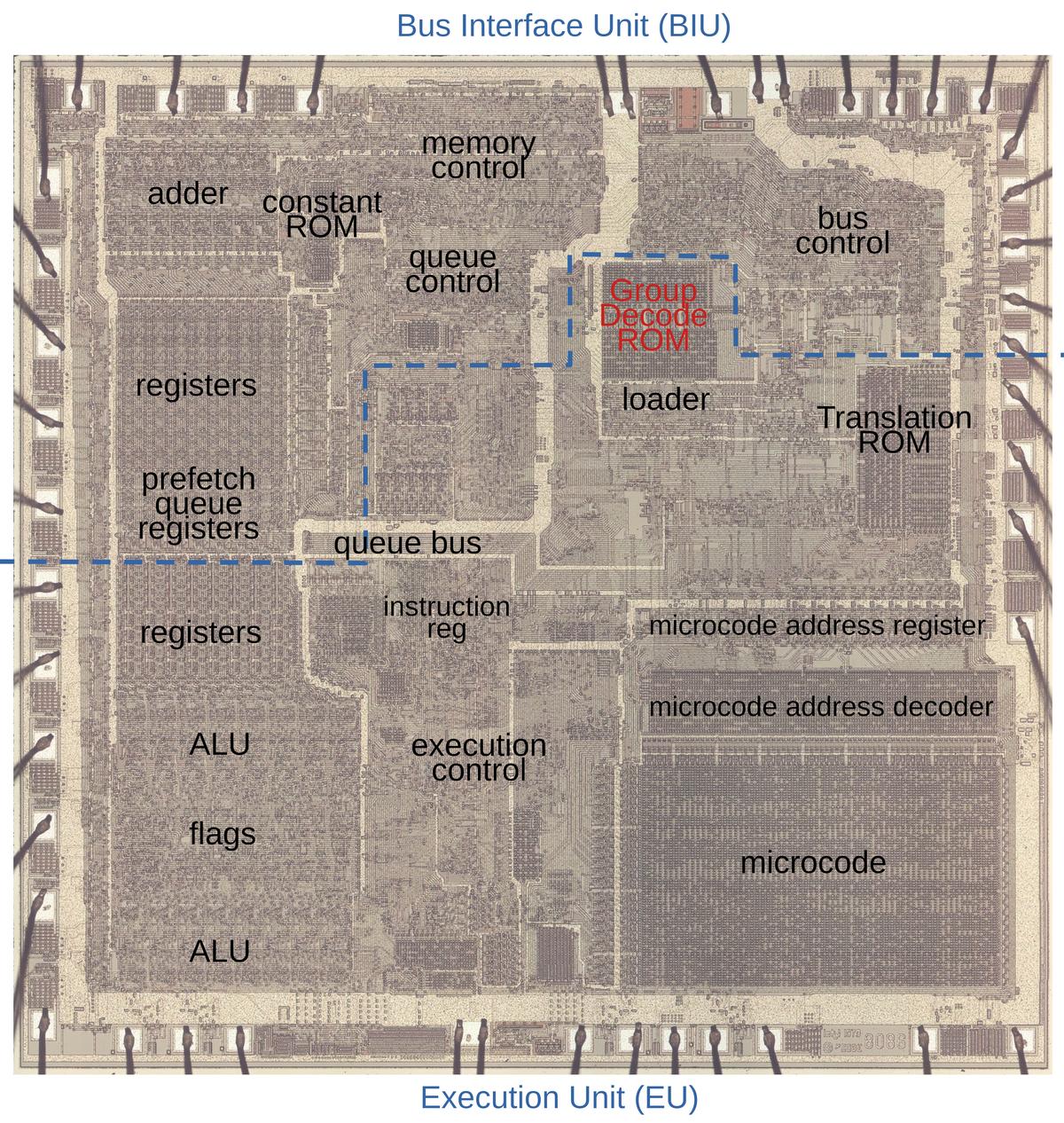
The diagram above shows the position of the Group Decode ROM on the silicon die, as well as other key functional blocks. The 8086 chip is partitioned into a Bus Interface Unit that communicates with external components such as memory, and the Execution Unit that executes instructions. Machine instructions are fetched from memory by the Bus Interface Unit and stored in the prefetch queue registers, which hold 6 bytes of instructions. To execute an instruction, the queue bus transfers an instruction byte from the prefetch queue to the instruction register, under control of a state machine called the Loader. Next, the Group Decode ROM categorizes the instruction according to its structure. In most cases, the machine instruction is implemented in low-level microcode. The instruction byte is transferred to the Microcode Address Register, where the Microcode Address Decoder selects the appropriate microcode routine that implements the instruction. The microcode provides the micro-instructions that control the Arithmetic/Logic Unit (ALU), registers, and other components to execute the instruction.
In this blog post, I will focus on a small part of this process: how the Group Decode ROM decodes instructions. Be warned that this post gets down into the weeds, so you might want to start with one of my higher-level posts, such as how the 8086's microcode engine works.
Microcode
Most instructions in the 8086 are implemented in microcode. Most people think of machine instructions as the basic steps that a computer performs. However, many processors have another layer of software underneath: microcode. With microcode, instead of building the CPU's control circuitry from complex logic gates, the control logic is largely replaced with code. To execute a machine instruction, the computer internally executes several simpler micro-instructions, specified by the microcode.
Microcode is only used if the Group Decode ROM indicates that the instruction is implemented in microcode. In that case, the microcode address register is loaded with the instruction and the address decoder selects the appropriate microcode routine. However, there's a complication. If the second byte of the instruction is a Mod R/M byte, the Group Decode ROM indicates this and causes a memory addressing micro-subroutine to be called.
Some simple instructions are implemented entirely in hardware and don't use microcode. These are known as 1-byte logic instructions (1BL) and are also indicated by the Group Decode ROM.
The Group Decode ROM's structure
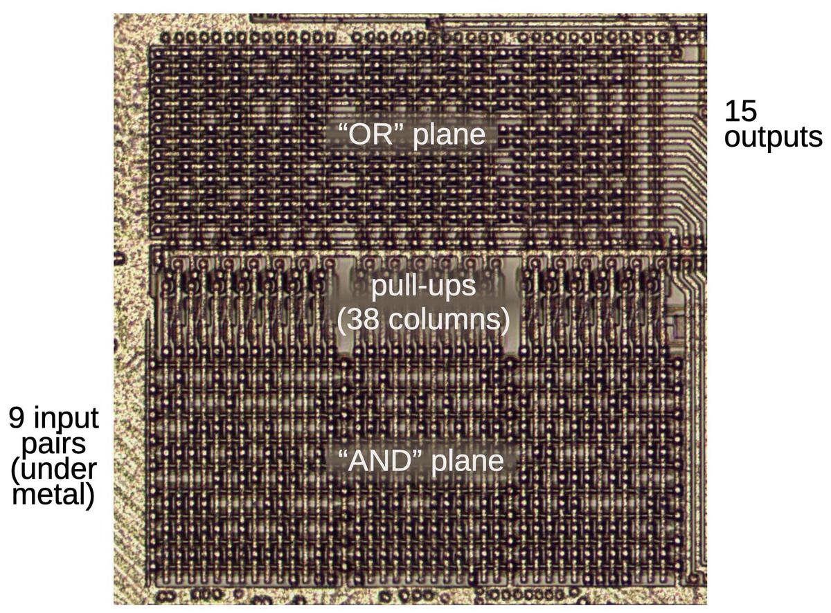
The Group Decode ROM takes an 8-bit instruction as input, along with an interrupt signal. It produces 15 outputs that control how the instruction is handled. In this section I'll discuss the physical implementation of the Group Decode ROM; the various outputs are discussed in a later section.
Although the Group Decode ROM is called a ROM, its implementation is really a PLA (Programmable Logic Array),
two levels of highly-structured logic gates.1
The idea of a PLA is to create two levels of NOR gates, each in a grid.
This structure has the advantages that it implements the logic densely and is easy to modify.
Although physically two levels of NOR gates, a PLA can be thought of as an AND layer followed by an OR layer.
The AND layer matches particular bit patterns and then the OR layer combines multiple values from the first
layer to produce arbitrary outputs.
Since the output values are highly structured, a PLA implementation is considerably more efficient than a ROM, since in a sense it combines multiple entries. In the case of the Group Decode ROM, using a ROM structure would require 256 columns (one for each 8-bit instruction pattern), while the PLA implementation requires just 36 columns, about 1/7 the size.
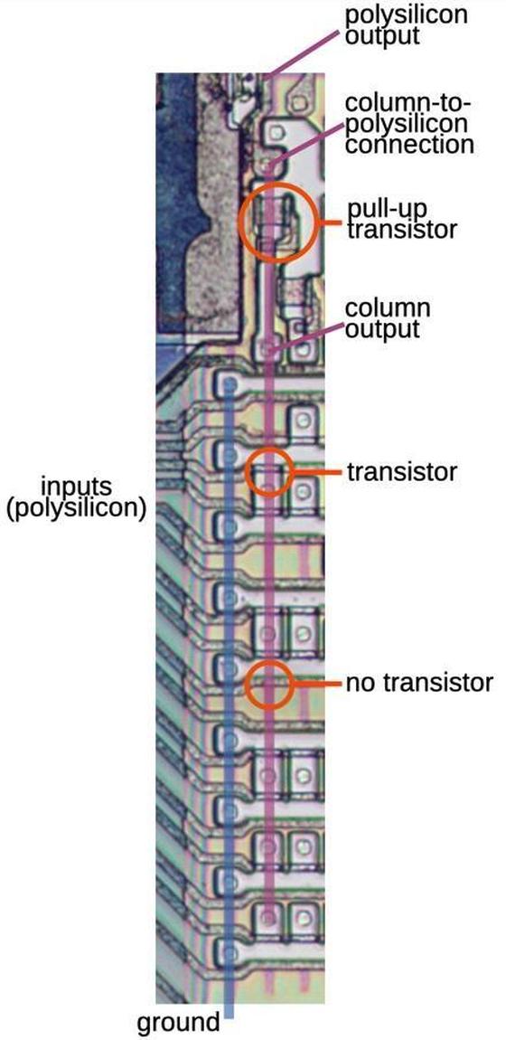
The diagram below shows how one column of the Group Decode ROM is wired in the "AND" plane. In this die photo, I removed the metal layer with acid to reveal the polysilicon and silicon underneath. The vertical lines show where the metal line for ground and the column output had been. The basic idea is that each column implements a NOR gate, with a subset of the input lines selected as inputs to the gate. The pull-up resistor at the top pulls the column line high by default. But if any of the selected inputs are high, the corresponding transistor turns on, connecting the column line to ground and pulling it low. Thus, this implements a NOR gate. However, it is more useful to think of it as an AND of the complemented inputs (via De Morgan's Law): if all the inputs are "correct", the output is high. In this way, each column matches a particular bit pattern.
The structure of the ROM is implemented through the silicon doping pattern, which is visible above. A transistor is formed where a polysilicon wire crosses a doped silicon region: the polysilicon forms the gate, turning the transistor on or off. At each intersection point, a transistor can be created or not, depending on the doping pattern. If a particular transistor is created, then the corresponding input must be 0 to produce a high output.
At the top of the diagram above, the column outputs are switched from the metal layer to polysilicon wires and become the inputs to the upper "OR" plane. This plane is implemented in a similar fashion as a grid of NOR gates. The plane is rotated 90 degrees, with the inputs vertical and each row forming an output.
Intermediate decoding in the Group Decode ROM
The first plane of the Group Decode ROM categorizes instructions into 36 types based on the instruction bit pattern.2
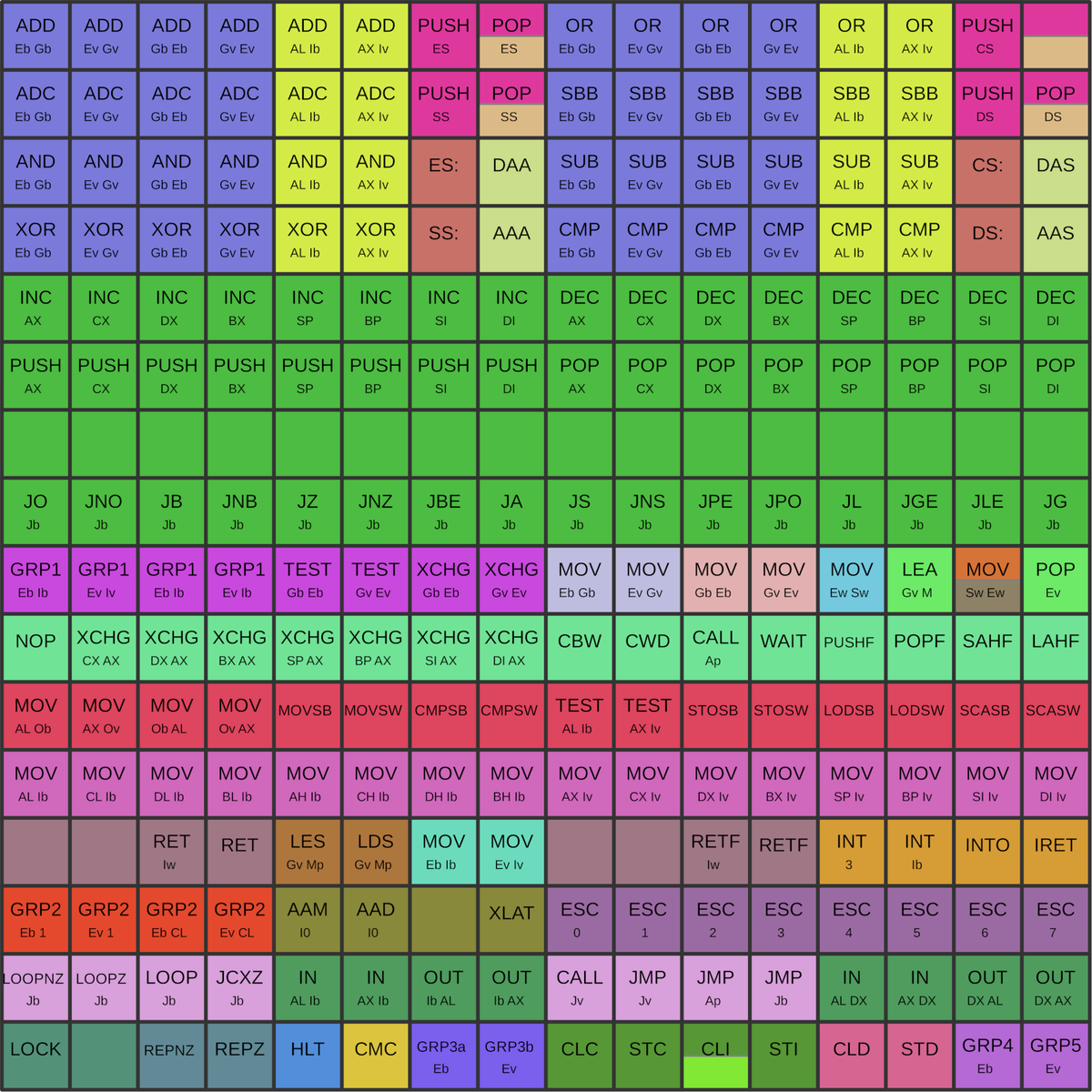
The table below shows the 256 instruction values, colored according to their categorization.3
For instance, the first blue block consists of the 32 ALU instructions
corresponding to the bit pattern 00XXX0XX, where X indicates that the bit can be 0 or 1.
These instructions are all decoded and executed in a similar way.
Almost all instructions have a single category, that is, they activate a single column line in the Group Decode ROM. However, a few instructions activate two lines and have two colors below.
Note that the instructions do not have arbitrary numeric opcodes, but are assigned in a way that makes decoding simpler. Because these blocks correspond to bit patterns, there is little flexibility. One of the challenges of instruction set design for early microprocessors was to assign numeric values to the opcodes in a way that made decoding straightforward. It's a bit like a jigsaw puzzle, fitting the instructions into the 256 available values, while making them easy to decode.
Outputs from the Group Decode ROM
The Group Decode ROM has 15 outputs, one for each row of the upper half. In this section, I'll briefly discuss these outputs and their roles in the 8086. For an interactive exploration of these signals, see this page, which shows the outputs that are triggered by each instruction.
Out 0 indicates an IN or OUT instruction.
This signal controls the M/IO (S2) status line, which distinguishes between a memory read/write and an I/O read/write.
Apart from this, memory and I/O accesses are basically the same.
Out 1 indicates (inverted) that the instruction has a Mod R/M byte and performs a read/modify/write on its argument. This signal is used by the Translation ROM when dispatching
an address handler (details).
(This signal distinguishes between, say, ADD [AX],BX and MOV [AX],BX.
The former both reads and writes [AX], while the latter only writes to it.)
Out 2 indicates a "group 3/4/5" opcode, an instruction where the second byte specifies the particular instruction, and thus decoding needs to wait for the second byte. This controls the loading of the microcode address register.
Out 3 indicates an instruction prefix (segment, LOCK, or REP).
This causes the next byte to be decoded as a new instruction, while blocking interrupt handling.
Out 4 indicates (inverted) a two-byte ROM instruction (2BR), i.e. an instruction is handled by the microcode ROM, but requires the second byte for decoding. This is an instruction with a Mod R/M byte. This signal controls the loader indicating that it needs to fetch the second byte. This signal is almost the same as output 1 with a few differences.
Out 5 specifies the top bit for an ALU operation. The 8086 uses a 5-bit field to specify an ALU operation.
If not specified explicitly by the microcode, the field uses bits 5 through 3 of the opcode.
(These bits distinguish, say, an ADD instruction from AND or SUB.)
This control line sets the top bit of the ALU field for instructions such as DAA, DAS, AAA, AAS, INC, and DEC that fall into a different set from the "regular" ALU instructions.
Out 6 indicates an instruction that sets or clears a condition code directly: CLC, STC, CLI, STI, CLD, or STD (but not CMC). This signal is used by the flag circuitry to update the condition code.
Out 7 indicates an instruction that uses the AL or AX register, depending on the instruction's size bit.
(For instance MOVSB vs MOVSW.)
This signal is used by the register selection circuitry, the M register specifically.
Out 8 indicates a MOV instruction that uses a segment register.
This signal is used by the register selection circuitry, the N register specifically.
Out 9 indicates the instruction has a d bit, where bit 1 of the instruction swaps the source and destination.
This signal is used by the register selection circuitry, swapping the roles of the M and N registers according to the d bit.
Out 10 indicates a one-byte logic (1BL) instruction, a one-byte instruction that is implemented in logic, not microcode. These instructions are the prefixes, HLT, and the condition-code instructions.
This signal controls the loader, causing it to move to the next instruction.
Out 11 indicates instructions where bit 0 is the byte/word indicator. This signal controls the register handling and the ALU functionality.
Out 12 indicates an instruction that operates only on a byte: DAA, DAS, AAA, AAS, AAM, AAD, and XLAT.
This signal operates in conjunction with the previous output to select a byte versus word.
Out 13 forces the instruction to use a byte argument if instruction bit 1 is set, overriding the regular byte/word pattern. Specifically, it forces the L8 (length 8 bits) condition
for the JMP direct-within-segment and the ALU instructions that are immediate with sign extension (details).
Out 14 allows a carry update. This prevents the carry from being updated by the INC and DEC operations.
This signal is used by the flag circuitry.
Columns
Most of the Group Decode ROM's column signals are used to derive the outputs listed above. However, some column outputs are also used as control signals directly. These are listed below.
Column 10 indicates an immediate MOV instruction. These instructions use instruction bit 3 (rather than bit 1) to select byte versus word, because the three low bits specify the register.
This signal affects the L8 condition described earlier and also causes the M register selection to be converted from a word register to a byte register if necessary.
Column 12 indicates an instruction with bits 5-3 specifying the ALU instruction.
This signal causes the X register to be loaded with
the bits in the instruction that specify the ALU operation. (To be precise, this signal prevents the X register
from being reloaded from the second instruction byte.)
Column 13 indicates the CMC (Complement Carry) instruction. This signal is used by the flags circuitry to complement the carry flag (details).
Column 14 indicates the HLT (Halt) instruction. This signal stops instruction processing by blocking the instruction queue.
Column 31 indicates a REP prefix. This signal causes the REPZ/NZ latch to be loaded with instruction bit 0 to
indicate if the prefix is REPNZ or REPZ. It also sets the REP latch.
Column 32 indicates a segment prefix. This signal loads the segment latches with the desired segment type.
Column 33 indicates a LOCK prefix. It sets the LOCK latch, locking the bus.
Column 34 indicates a CLI instruction. This signal immediately blocks interrupt handling to avoid an interrupt between the CLI instruction and when the interrupt flag bit is cleared.
Timing
One important aspect of the Group Decode ROM is that its outputs are not instantaneous.
It takes a clock cycle to get the outputs from the Group Decode ROM.
In particular, when instruction decoding starts, the timing signal FC (First Clock) is activated to indicate the first clock
cycle. However, the Group Decode ROM's outputs are not available until the Second Clock SC.
One consequence of this is that even the simplest instruction (such as a flag operation) takes two clock cycles, as does a prefix. The problem is that even though the instruction could be performed in one clock cycle, it takes two clock cycles for the Group Decode ROM to determine that the instruction only needs one cycle. This illustrates how a complex instruction format impacts performance.
The FC and SC timing signals are generated by a state machine called the Loader.
These signals may seem trivial, but there are a few complications.
First, the prefetch queue may run empty, in which case the FC and/or SC signal is delayed until the prefetch queue has a byte available.
Second, to increase performance, the 8086 can start decoding an instruction during the last clock cycle of the previous instruction.
Thus, if the microcode indicates that there is one cycle left, the Loader can proceed with the next instruction.
Likewise, for a one-byte instruction implemented in hardware (one-byte logic or 1BL), the loader proceeds
as soon as possible.
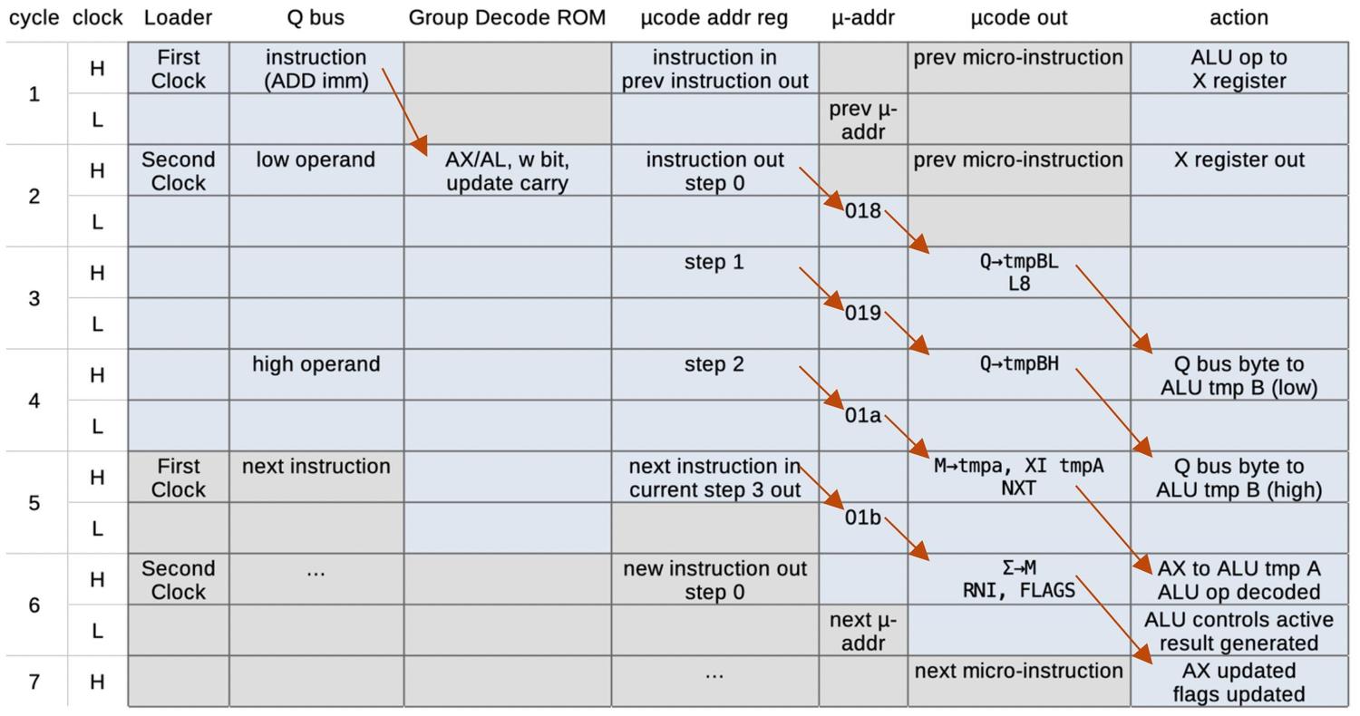
The diagram below shows the timing of an ADD instruction. Each line is half of a clock cycle.
Execution is pipelined: the instruction is fetched during the first clock cycle (First Clock).
During Second Clock, the Group Decode ROM produces its output. The microcode address register also generates
the micro-address for the instruction's microcode.
The microcode ROM supplies a micro-instruction during the third clock cycle and execution of the micro-instruction
takes place during the fourth clock cycle.
The Group Decode ROM's outputs during Second Clock control the decoding.
Most importantly, the ADD imm instruction used microcode; it is not a one-byte logic instruction (1BL).
Moreover, it does not have a Mod R/M byte, so it does not need two bytes for decoding (2BR).
For a 1BL instruction, microcode execution would be blocked and the next instruction would be immediately fetched.
On the other hand, for a 2BR instruction, the loader would tell the prefetch queue that it was done with the
second byte during the second half of Second Clock.
Microcode execution would be blocked during the third cycle and the fourth cycle would execute a microcode
subroutine to determine the memory address.
For more details, see my article on the 8086 pipeline.
Interrupts
The Group Decode ROM takes the 8 bits of the instruction as inputs, but it has an additional input indicating that an interrupt is being handled. This signal blocks most of the Group Decode ROM outputs. This prevents the current instruction's outputs from interfering with interrupt handling. I wrote about the 8086's interrupt handling in detail here, so I won't go into more detail in this post.
Conclusions
The Group Decode ROM indicates one of the key differences between CISC processors (Complex Instruction Set Computer) such as the 8086 and the RISC processors (Reduced Instruction Set Computer) that became popular a few years later. A RISC instruction set is designed to make instruction decoding very easy, with a small number of uniform instruction forms. On the other hand, the 8086's CISC instruction set was designed for compactness and high code density. As a result, instructions are squeezed into the available opcode space. Although there is a lot of structure to the 8086 opcodes, this structure is full of special cases and any patterns only apply to a subset of the instructions. The Group Decode ROM brings some order to this chaotic jumble of instructions, and the number of outputs from the Group Decode ROM is a measure of the instruction set's complexity.
The 8086's instruction set was extended over the decades to become the x86 instruction set in use today.
During that time, more layers of complexity were added to the instruction set.
Now, an x86 instruction can be up to 15 bytes long with multiple prefixes.
Some prefixes change the register encoding or indicate a completely different instruction set such as VEX (Vector Extensions) or SSE (Streaming SIMD Extensions).
Thus, x86 instruction decoding is very difficult, especially when trying to decode multiple instructions in parallel.
This has an impact in modern systems, where x86 processors typically have 4 complex instruction decoders while Apple's ARM processors have 8 simpler decoders; this is said to give Apple a performance benefit.
Thus, architectural decisions from 45 years ago are still impacting the performance of modern processors.
I've written numerous posts on the 8086 so far and plan to continue reverse-engineering the 8086 die so follow me on Twitter @kenshirriff or RSS for updates. I've also started experimenting with Mastodon recently as @[email protected]. Thanks to Arjan Holscher for suggesting this topic.
Notes and references
-
You might wonder what the difference is between a ROM and a PLA. Both of them produce arbitrary outputs for a set of inputs. Moreover, you can replace a PLA with a ROM or vice versa. Typically a ROM has all the input combinations decoded, so it has a separate row for each input value, i.e. 2N rows. So you can think of a ROM as a fully-decoded PLA.
Some ROMs are partially decoded, allowing identical rows to be combined and reducing the size of the ROM. This technique is used in the 8086 microcode, for instance. A partially-decoded ROM is fairly similar to a PLA, but the technical distinction is that a ROM has only one output row active at a time, while a PLA can have multiple output rows active and the results are OR'd together. (This definition is from The Architecture of Microprocessors p117.)
The Group Decode ROM, however, has a few cases where multiple rows are active at the same time (for instance the segment register
POPinstructions). Thus, the Group Decode ROM is technically a PLA and not a ROM. This distinction isn't particularly important, but you might find it interesting. ↩ -
The Group Decode ROM has 38 columns, but two columns (11 and 35) are unused. Presumably, these were provided as spares in case a bug fix or modification required additional decoding. ↩
-
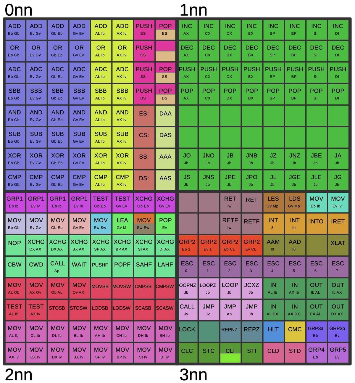
Like the 8008 and 8080, the 8086's instruction set was designed around a 3-bit octal structure. Thus, the 8086 instruction set makes much more sense if viewed in octal instead of hexadecimal. The table below shows the instructions with an octal organization. Each 8×8 block uses the two low octal digits, while the four large blocks are positioned according to the top octal digit (labeled). As you can see, the instruction set has a lot of structure that is obscured in the usual hexadecimal table.
The 8086 instruction set, put in a table according to the octal opcode value.For details on the octal structure of the 8086 instruction set, see The 80x86 is an Octal Machine. ↩
3 comments:
Thinking about how complicated is decoding on 8086, the decoding on current x86 processors must be a real nightmare, taking into account that there is more than 2000 instructions
Eliminate what is merely operand variation (B/W/D/Q, SH/SS/SD/PH/PS/PD, etc.) and you drop to a few hundred.
Eliminate what is merely operation variation (ADD/SUB/MUL/DIV, SHL/SHR/ROL/ROR, condition codes, etc.) and you drop further.
Ken's article nicely illustrates it... and yes, what worked for the 8086 way back when, still works for x86 like a charm today.
So no, x86 decoding is not this ugly nightmare that everyone who has never designed an x86 decoder makes it out to be. :-)
Note that the same is true for its often bashed variable length encoding, i.e. the "x86 decode is width- and power-limited" myth.
Case in point: look at the 3-wide decoder block in recent/current/upcoming Atom cores... and how it can be replicated 1x, 2x, 3x, etc.
Long story short: x86 decode isn't terrible... once you are skilled in the art. Heck, it will be interesting to see what ML can do for it...
Why is pop ev instruction on 0x8f opcode, why not GRP5?
Post a Comment