In this article, I take a close look at the "standard cells" used in the 386, the logic blocks that were arranged and wired by software. Reverse-engineering these circuits shows how standard cells implement logic gates, latches, and other components with CMOS transistors. Modern integrated circuits still use standard cells, much smaller now, of course, but built from the same principles.
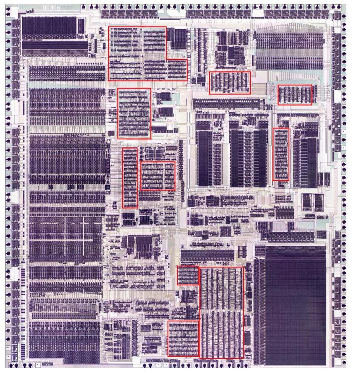
The photo below shows the 386 die with the automatic-place-and-route regions highlighted in red. These blocks of unstructured logic have cells arranged in rows, giving them a characteristic striped appearance. In comparison, functional blocks such as the datapath on the left and the microcode ROM in the lower right were designed manually to optimize density and performance, giving them a more solid appearance. As for other features on the chip, the black circles around the border are bond wire connections that go to the chip's external pins. The chip has two metal layers, a small number by modern standards, but a jump from the single metal layer of earlier processors such as the 286. The metal appears white in larger areas, but purplish where circuitry underneath roughens its surface. For the most part, the underlying silicon and the polysilicon wiring on top are obscured by the metal layers.
Early processors in the 1970s were usually designed by manually laying out every transistor individually, fitting transistors together like puzzle pieces to optimize their layout. While this was tedious, it resulted in a highly dense layout. Federico Faggin, designer of the popular Z80 processor, describes finding that the last few transistors wouldn't fit, so he had to erase three weeks of work and start over. The closeup of the resulting Z80 layout below shows that each transistor has a different, complex shape, optimized to pack the transistors as tightly as possible.2
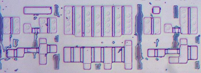
Standard-cell logic is an alternative that is much easier than manual layout.3 The idea is to create a standard library of blocks (cells) to implement each type of gate, flip-flop, and other low-level component. To use a particular circuit, instead of arranging each transistor, you use the standard design. Each cell has a fixed height but the width varies as needed, so the standard cells can be arranged in rows. For example, the die photo below three cells in a row: a latch, a high-current inverter, and a second latch. This region has 24 transistors in total with PMOS above and NMOS below. Compare the orderly arrangement of these transistors with the Z80 transistors above.
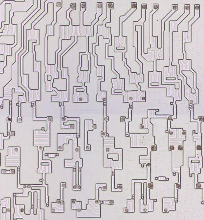
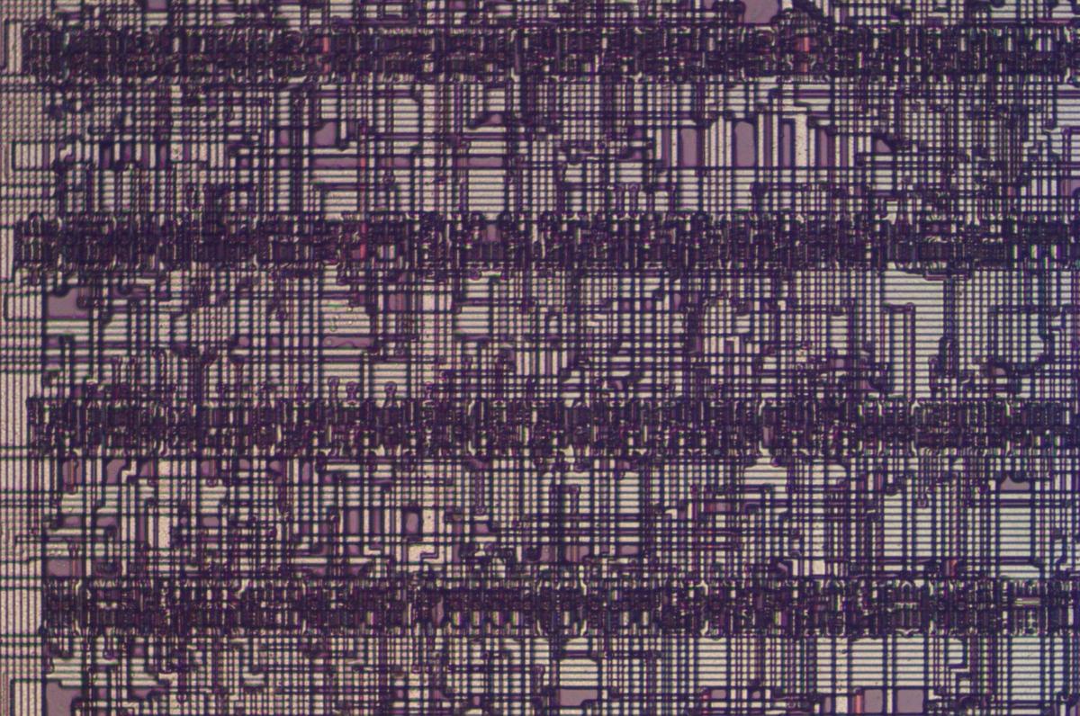
The space between rows is used as a "wiring channel" that holds the wiring between the cells. The photo below zooms out to show four rows of standard cells (the dark bands) and the wiring in between. The 386 uses three layers for this wiring: polysilicon and the upper metal layer (M2) for vertical segments and the lower metal layer (M1) for horizontal segments.
To summarize, with standard cell logic, the cells are obtained from the standard cell library as needed, defining the transistor layout and the wiring inside the cell. However, the locations of each cell (placing) need to be determined, as well as how to arrange the wiring (routing). As will be seen, placing and routing the cells can be done manually or automatically.
Use of standard cells in the 386
Fairly late in the design process, the 386 team decided to use automatic place and route for parts of the chip. By using automatic place and route, 2,254 gates (consisting of over 10,000 devices) were placed and routed in seven weeks. (These numbers are from a paper "Automatic Place and Route Used on the 80386", co-written by Pat Gelsinger, now the CEO of Intel. I refer to this paper multiple times, so I'll call it APR386 for convenience.4) Automatic place and route was not only faster, but it avoided the errors that crept in when layout was performed manually.5
The "place" part of automatic place and route consists of determining the arrangement of the standard cells into rows to minimize the distance between connected cells. Running long wires between cells wastes space on the die, since you end up with a lot of unnecessary metal wiring. But more importantly, long paths have higher resistance, slowing down the signals. Placement is a difficult optimization problem that is NP-complete. Moreover, the task was made more complicated by weighting paths by importance and electrical characteristics, classifying signals as "normal", "fast", or "critical". Paths were also weighted to encourage the use of the thicker M2 metal layer rather than the lower M1 layer.
The 386 team solved the placement problem with a program called Timberwolf, developed by a Berkeley grad student. As one member of the 386 team said, "If management had known that we were using a tool by some grad student as a key part of the methodology, they would never have let us use it." Timberwolf used a simulated annealing algorithm, based on a simulated temperature that decreased over time. The idea is to randomly move cells around, trying to find better positions, but gradually tighten up the moves as the "temperature" drops. At the end, the result is close to optimal. The purpose of the temperature is to avoid getting stuck in a local minimum by allowing "bad" changes at the beginning, but then tightening up the changes as the algorithm progresses.
Once the cells were placed in their positions, the second step was "routing", generating the layout of all the wiring. A suitable commercial router was not available in 1984, so Intel developed its own. As routing is a difficult problem (also NP-complete), they took an iterative heuristic approach, repeatedly routing until they found the smallest channel height that would work. (Thus, the wiring channels are different sizes as needed.) Then they checked the R-C timing of all the signals to find any signals that were too slow. Designers could boost the size of the associated drivers (using the variety of available standard cells) and try the routing again.
Brief CMOS overview
The 386 was the first processor in Intel's x86 line to be built with a technology called CMOS instead of using NMOS. Modern processors are all built from CMOS because CMOS uses much less power than NMOS. CMOS is more complicated to construct, though, because it uses two types of transistors—NMOS and PMOS—so early processors were typically NMOS. But by the mid-1980s, the advantages of switching to CMOS were compelling.
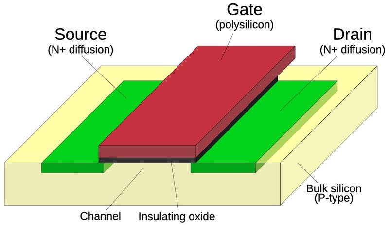
The diagram below shows how an NMOS transistor is constructed. The transistor can be considered a switch between the source and drain, controlled by the gate. The source and drain regions (green) consist of silicon doped with impurities to change its semiconductor properties, forming N+ silicon. The gate consists of a layer of polysilicon (red), separated from the silicon by a very thin insulating oxide layer. Whenever polysilicon crosses active silicon, a transistor is formed. A PMOS transistor has similar construction except it swaps the N-type and P-type silicon, consisting of P+ regions in a substrate of N silicon.
The NMOS and PMOS transistors are opposite in their construction and operation. An NMOS transistor turns on when the gate is high, while a PMOS transistor turns on when the gate is low. An NMOS transistor is best at pulling its output low, while a PMOS transistor is best at pulling its output high. In a CMOS circuit, the transistors work as a team, pulling the output high or low as needed; this is the "Complementary" in CMOS. (The behavior of MOS transistors is complicated, so this description is simplified, just enough to understand digital circuits.)
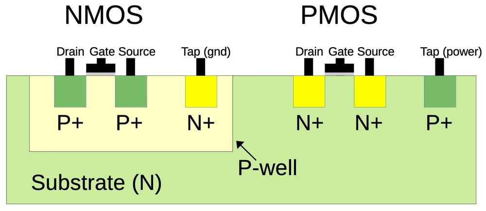
One complication is that NMOS transistors are built on P-type silicon, while PMOS transistors are built on N-type silicon. Since the silicon die itself is N silicon, the NMOS transistors need to be surrounded by a tub or well of P silicon.6 The cross-section diagram below shows how the NMOS transistor on the left is embedded in a well of P-type silicon.
For proper operation, the silicon that surrounds transistors needs to be connected to the appropriate voltage through "tap" contacts.7 For PMOS transistors, the substrate is connected to power through the taps, while for NMOS transistors the well region is connected to ground through the taps. The chip needs to have enough taps to keep the voltage from fluctuating too much; each standard cell typically has a positive tap and a ground tap.
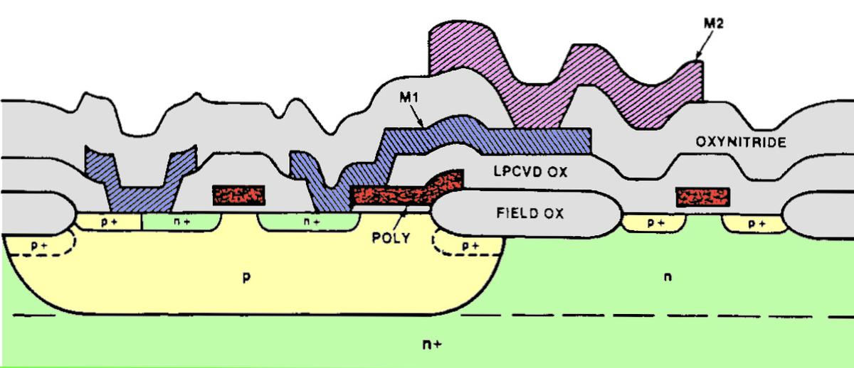
The actual structure of the integrated circuit is much more three-dimensional than the diagram above, due to the thickness of the various layers. The diagram below is a more accurate cross-section. The 386 has two layers of metal: the lower metal layer (M1) in blue and the upper metal layer (M2) in purple. Polysilicon is colored red, while the insulating oxide layers are gray.
This complicated three-dimensional structure makes it harder to interpret the microscope images. Moreover, the two metal layers obscure the circuitry underneath. I have removed various layers with acids for die photos, but even so, the images are harder to interpret than those of simpler chips. If the die photos look confusing, don't be surprised.
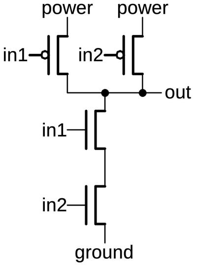
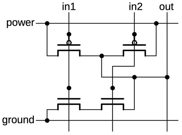
A logic gate in CMOS is constructed from NMOS and PMOS transistors working together. The schematic below shows a NAND gate with two PMOS transistors in parallel above and two NMOS transistors in series below. If both inputs are high, the two NMOS transistors turn on, pulling the output low. If either input is low, a PMOS transistor turns on, pulling the output high. (Recall that NMOS and PMOS are opposites: a high voltage turns an NMOS transistor on while a low voltage turns a PMOS transistor on.) Thus, the CMOS circuit below produces the desired output for the NAND function.
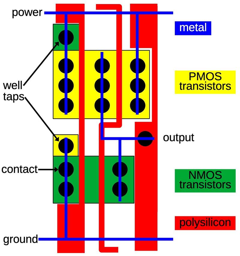
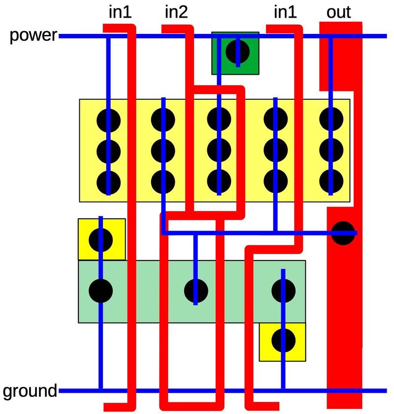
The diagram below shows how this NAND gate is implemented in the 386 as a standard cell.9 A lot is going on in this cell, but it boils down to four transistors, as in the schematic above. The yellow region is the P-type silicon that forms the two PMOS transistors; the transistor gates are where the polysilicon (red) crosses the yellow region.8 (The middle yellow region is the drain for both transistors; there is no discrete boundary between the transistors.) Likewise, the two NMOS transistors are at the bottom, where the polysilicon (red) crosses the active silicon (green). The blue lines indicate the metal wiring for the cell. I thinned these lines to make the diagram clearer; in the actual cell, the metal lines are as thick as they can be without touching, so they cover most of the cell. The black circles are contacts, connections between the metal and the silicon or polysilicon. Finally, the well taps are the opposite type of silicon, connected to the underlying silicon well or substrate to keep it at the proper voltage.
Wiring to a cell's inputs and output takes place at the top or bottom of the cell, with wiring in the channels between rows of cells. The polysilicon input and output lines are thickened at the top and bottom of the cell to allow connections to the cell. The wiring between cells can be done with either polysilicon or metal. Typically the upper metal layer (M2) is used for vertical wiring, while the lower metal layer (M1) is used for horizontal runs. Since each standard cell only uses M1, vertical wiring (M2) can pass over cells. Moreover, a cell's output can also use a vertical metal wire (M2) rather than the polysilicon shown. The point is that there is a lot of flexibility in how the system can route wires between the cells. The power and ground wires (M1) are horizontal so they can run from cell to cell and a whole row can be powered from the ends.
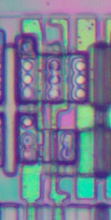
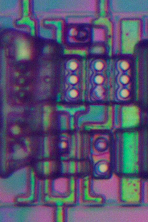
The photo below shows this NAND cell with the metal layers removed by acid, leaving the silicon and the polysilicon. You can match the features in the photo with the diagram above. The polysilicon appears green due to thin-film effects. At the bottom, two polysilicon lines are connected to the inputs.
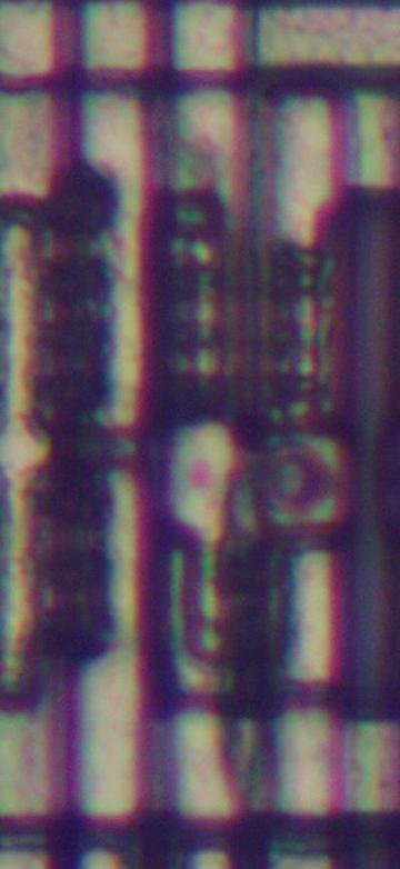
The photo below shows how the cell appears in the original die. The two metal layers are visible, but they hide the polysilicon and silicon underneath. The vertical metal stripes are the upper (M2) wiring while the lower metal wiring (M1) makes up the standard cell. It is hard to distinguish the two metal layers, which makes interpretation of the images difficult. Note that the metal wiring is wide, almost completely covering the cell, with small gaps between wires. The contacts are visible as dark circles. Is hard to recognize the standard cells from the bare die, as the contact pattern is the only distinguishing feature.
One of the interesting features of the 386's standard cell library is that each type of logic gate is available in multiple drive strengths. That is, cells are available with small transistors, large transistors, or multiple transistors in parallel. Because the wiring and the transistor gates have capacitance, a delay occurs when changing state. Bigger transistors produce more current, so they can switch the values on a wire faster. But there are two disadvantages to bigger transistors. First, they take up more space on the die. But more importantly, bigger transistors have bigger gates with more capacitance, so their inputs take longer to switch. (In other words, increasing the transistor size speeds up the output but slows the input, so overall performance could end up worse.) Thus, the sizes of transistors need to be carefully balanced to achieve optimum performance.10 With a variety of sizes in the standard cell library, designers can make the best choices.
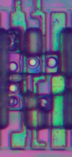
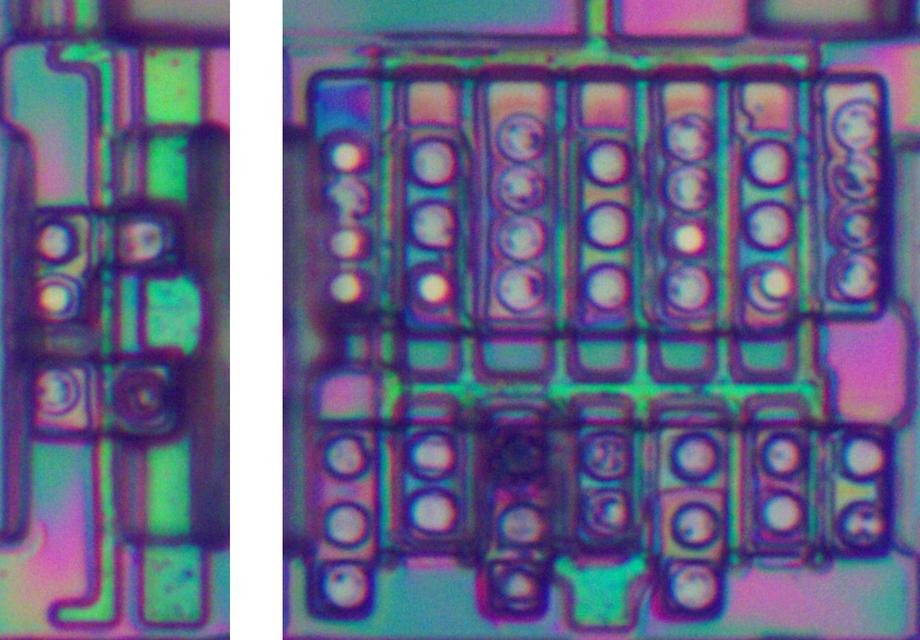
The image below shows a small NAND gate. The design is the same as the one described earlier, but the transistors are much smaller. (Note that there is one row of metal contacts instead of two or three.) The transistor gates are about half as wide (measured vertically) so the NAND gate will produce about half the output current.11
Since the standard cells are all the same height, the maximum size of a transistor is limited. To provide a larger drive strength, multiple transistors can be used in parallel. The NAND gate below uses 8 transistors, four PMOS and four NMOS, providing twice as much current.
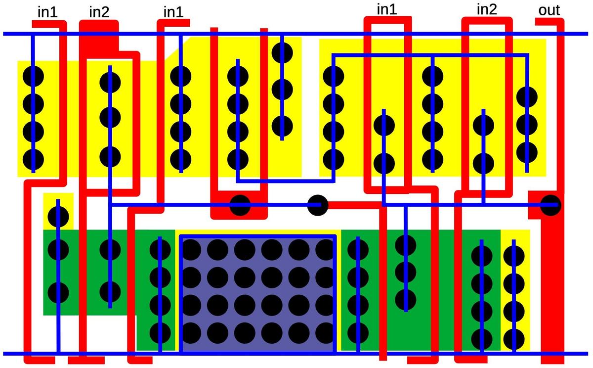
The diagram below shows the structure of the large NAND gate, essentially two NAND gates in parallel. Note that input 1 must be provided separately to both halves by the routing outside the cell. Input 2, on the other hand, only needs to be supplied to the cell once, since it is wired to both halves inside the cell.
Inverters are also available in a variety of drive strengths, from very small to very large, as shown below. The inverter on the left uses the smallest transistors, while the inverter on the right not only uses large transistors but is constructed from six inverters in parallel. One polysilicon input controls all the transistors.
A more complex standard cell is XOR. The diagram below shows an XOR cell with large drive current. (There are smaller XOR cells). As with the large NAND gate, the PMOS transistors are doubled up for more current. The multiple input connections are handled by the routing outside the cell. Since the NMOS transistors don't need to be doubled up, there is a lot of unused space in the lower part of the cell. The extra space is used for a very large tap contact, consisting of 24 contacts to ground the well.
XOR is a difficult gate to build with CMOS. The cell above implements it by combining a NOR gate and an AND-NOR gate, as shown below. You can verify that if both inputs are 0 or both inputs are 1, the output is forced low as desired. In the layout above, the NOR gate is on the left, while the AND-NOR gate has the AND part on the right. A metal wire down the center connects the NOR output to the AND-NOR input. The need for two sub-gates is another reason why the XOR cell is so large.
I'll describe one more cell, the latch, which holds one bit and is controlled by a clock signal. Latches are heavily used in the 386 whenever a signal needs to be remembered or a circuit needs to be synchronous. The 386 has multiple types of standard cell latches including latches with set or reset controls and latches with different drive strengths. Moreover, two latches can be combined to form an edge-triggered flip-flop standard cell.
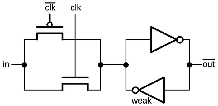
The schematic below shows the basic latch circuit, the most common type in the 386. On the right, two inverters form a loop. This loop can stably hold a 0 or 1 value. On the left, a PMOS transistor and an NMOS transistor form a transmission gate. If the clock is high, both transistors will turn on and pass the input through. If the clock is low, both transistors will turn off and block the input. The trick to the latch is that one inverter is weak, producing just a small current. The consequence is that the input can overpower the inverter output, causing the inverter loop to switch to the input value. The result is that when the clock is high, the latch will pass the input value through to the output. But when the clock is low, the latch will hold its previous value. (The output is inverted with respect to the input, which is slightly inconvenient but reduces the size of the latch.)
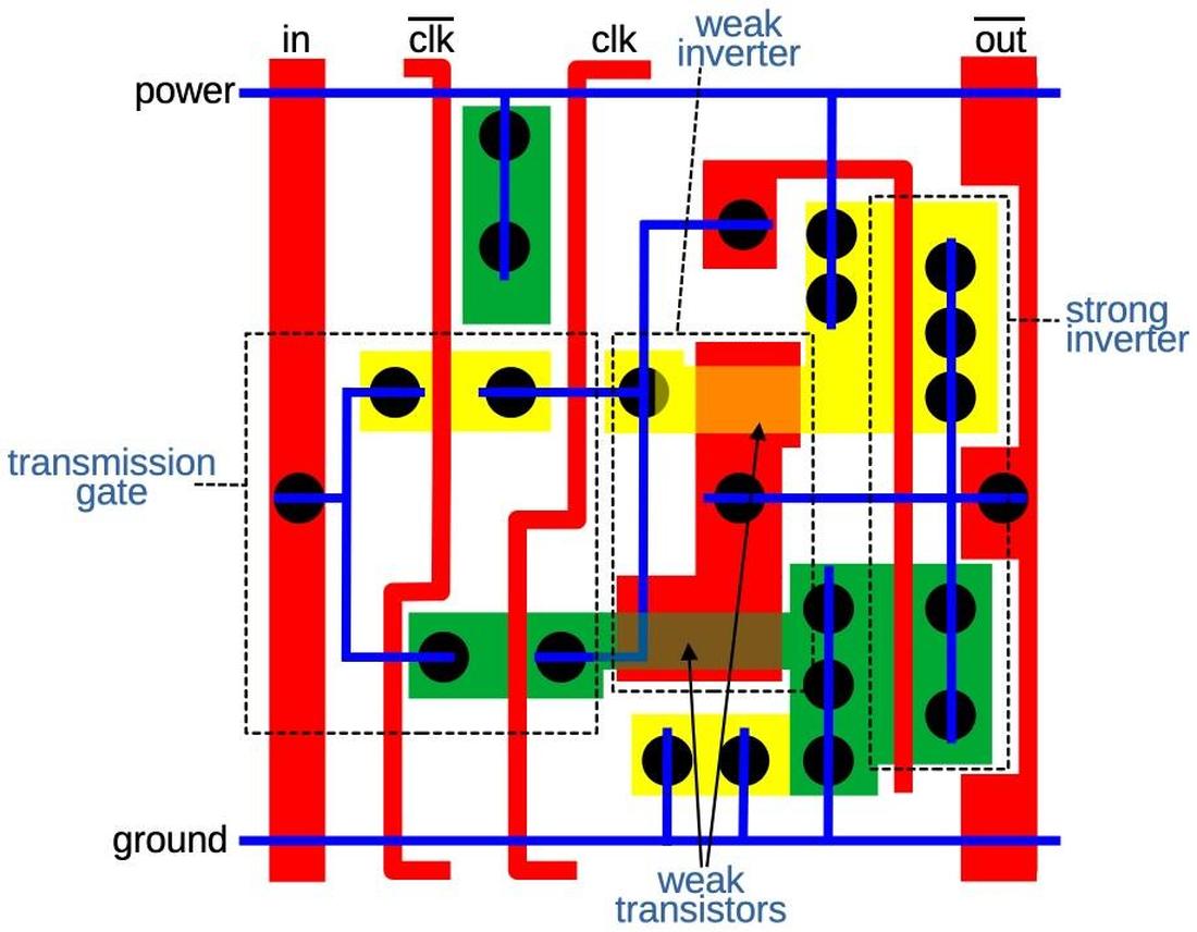
The standard cell layout of the latch (below) is complicated, but it corresponds to the schematic. At the left are the PMOS and NMOS transistors that form the transmission gate. In the center is the weak inverter, with its output to the left. The weak transistors are in the middle; they are overlapped by a thick polysilicon region, creating a long gate that produces a low current.12 At the right is the inverter that drives the output. The layout of this circuit is clever, designed to make the latch as compact as possible. For example, the two inverters share power and ground connections. Notice how the two clock lines pass from top to bottom through gaps in the active silicon so each line only forms one transistor. Finally, the metal line in the center connects the transmission gate outputs and the weak inverter output to the other inverter's input, but asymmetrically at the top so the two inverters don't collide.
To summarize, I examined many (but not all) of the standard cells in the 386 and found about 70 different types of cells. These included the typical logic gates with various drive strengths: inverters, buffers, XOR, XNOR, AND-NOR, and 3- and 4-input logic gates. There are also transmission gates including ones that default high or low, as well as multiplexers built from transmission gates. I found a few cells that were surprising such as dual inverters and a combination 3-input and 2-input NAND gate. I suspect these consist of two standard cells that were merged together, since they seem too specialized to be part of a standard cell library.
The APR386 paper showed six of the standard cells in the 386 with the diagram below. The small and large inverters are the same as the ones described above, as is the NAND gate NA2B. The latch is similar to the one described above, but with larger transistors. The APR386 paper also showed a block of standard cells, which I was able to locate in the 386.13
Intel's standard cell line
Intel productized its standard cells around 1986 as a 1.5 µm library using Intel's CMOS technology (called CHMOS III).14 Although the library had over 100 cell types, it was very limited compared to the cells used inside the 386. The library included logic gates, flip-flops, and latches as well as scalable registers, counters, and adders. Most gates only came in one drive strength. Even inverters only came in "normal" and "high" drive strength. I assume these cells are the same as the ones used in the 386, but I don't have proof. The library also included larger devices such as a cell-compatible 80C51 microcontroller and PC peripheral chips such as the 8259 programmable interrupt controller and the 8254 programmable interval timer. I think these were re-implemented using standard cells.
Intel later produced a 1.0 µm library using CHMOS IV, for use "both by ASIC customers and Intel's internal chip designers." This library had a larger collection of drive strengths. The 1.0 µm library included the 80C186 and associated peripheral chips.
Layout techniques in the 386
In this section, I'll look at the active silicon regions, making the cells themselves more visible. In the photos below, I dissolved the metal and polysilicon, leaving the active silicon. (Ignore the irregular greenish shapes; these are oxide that wasn't fully removed.)
The photo below shows the silicon for three rows of standard cells using automatic place and route. You can see the wide variety of standard cell widths, but the height of the cells is constant. The transistor gates are visible as the darker vertical stripes across the silicon. You may be able to spot the latch in each row, distinguished by the long, narrow transistors of the weak inverters.
In the first row, the larger PMOS transistors are on top, while the smaller NMOS transistors are below. This pattern alternates from row to row, so the second row has the NMOS transistors on top and the third row has the PMOS transistors on top. The height of the wiring channel between the cells is variable, made as small as possible while fitting the wiring.
The 386 also contains regions of standard cells that were apparently manually placed and routed, as shown in the photo below. Using standard cells avoids the effort of laying out each transistor, so it is still easier than a fully custom layout. These cells are in rows, but the rows are now double rows with channels in between. The density is higher, but routing the wires becomes more challenging.
For critical circuitry such as the datapath, the layout of each transistor was optimized. The register file, for example, has a very dense layout as shown below. As you can see, the density is much higher than in the previous photos. (The three photos are at the same scale.) Transistors are packed together with very little wasted space. This makes the layout difficult since there is little room for wiring. For this particular circuit, the lower metal layer (M1) runs vertically with signals for each bit while the upper metal layer (M2) runs horizontally for power, ground, and control signals.15
The point of this is that the 386 uses a variety of different design techniques, from dense manual layout to much faster automated layout. Different techniques were used for different parts of the chip, based on how important it was to optimize. For example, circuits in the datapath were typically repeated 32 times, once for each bit, so manual effort was worthwhile. The most critical functional blocks were the microcode ROM (CROM), large PLAs, ALU, TLB (translation lookaside buffer), and the barrel shifter.16
Conclusions
Standard cell logic and automatic place and route have a long history before the 386, back to the early 1970s, so this isn't an Intel invention.17 Nonetheless, the 386 team deserves the credit for deciding to use this technology at a time when it was a risky decision. They needed to develop custom software for their placing and routing needs, so this wasn't a trivial undertaking. This choice paid off and they completed the 386 ahead of schedule. The 386 ended up being a huge success for Intel, moving the x86 architecture to 32-bits and defining the dominant computer architecture for the rest of the 20th century.
If you're interested in standard cell logic, I wrote about standard cell logic in an IBM chip. I plan to write more about the 386, so follow me on Twitter @kenshirriff or RSS for updates. I'm also on Mastodon occasionally as @[email protected]. Thanks to Pat Gelsinger and Roxanne Koester for providing helpful papers.
Notes and references
-
The decision to use automatic place and route is described on page 13 of the Intel 386 Microprocessor Design and Development Oral History Panel, a very interesting document on the 386 with discussion from some of the people involved in its development. ↩
-
Circuits that had a high degree of regularity, such as the arithmetic/logic unit (ALU) or register storage were typically constructed by manually laying out a block to implement a bit and then repeating the block as needed. Because a circuit was repeated 32 times for the 32-bit processor, the additional effort was worthwhile. ↩
-
An alternative layout technique is the gate array, which doesn't provide as much flexibility as a standard cell approach. In a gate array (sometimes called a master slice), the chip had a fixed array of transistors (and often resistors). The chip could be customized for a particular application by designing the metal layer to connect the transistors as needed. The density of the chip was usually poor, but gate arrays were much faster to design, so they were advantageous for applications that didn't need high density or produced a relatively small volume of chips. Moreover, manufacturing was much faster because the silicon wafers could be constructed in advance with the transistor array and warehoused. Putting the metal layer on top for a particular application could then be quick. Similar gate arrays used a fixed arrangement of logic gates or flip-flops, rather than transistors. Gate arrays date back to 1967. ↩
-
The full citation for the APR386 paper is "Automatic Place and Route Used on the 80386" by Joseph Krauskopf and Pat Gelsinger, Intel Technology Journal, Spring 1986. I was unable to find it online. ↩
-
Once the automatic place and route process had finished, the mask designers performed some cleanup along with compaction to squeeze out wasted space, but this was a relatively minor amount of work.
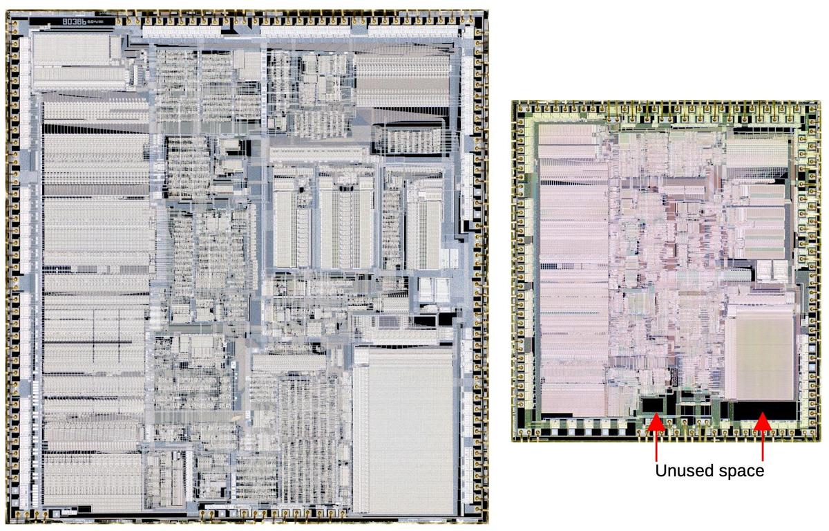
While manual optimization has benefits, it can also be overdone. When the manufacturing process improved, the 80386 moved from a 1.5 µm process to a 1 µm process. The layout engineers took advantage of this switch to optimize the standard cell circuitry, manually squeezing out some extra space. Unfortunately, optimizing one block of a die doesn't necessarily make the die smaller, since the size is constrained by the largest blocks. The result is that the optimized 80386 has blocks of empty space at the bottom (visible as black rectangles) and the standard-cell optimization didn't provide any overall benefit. (As the Pentium Pro chief architect Robert Colwell explains, "Removing the state of Kansas does not make the perimeter of the United States any smaller.")
Comparison of the 1.5 µm die and the 1 µm die at the same scale. Photos courtesy of Antoine Bercovici.At least compaction went better for the 386 than for the Pentium. Intel performed a compaction on the Pentium shortly before release, attempting to reduce the die size. The engineers shrunk the floating point divider, removing some lookup table cases that they proved were unnecessary. Unfortunately, the proof was wrong, resulting in floating point errors in a few cases. This caused the infamous Pentium FDIV bug, a problem that became highly visible to the general public. Replacing the flawed processors cost Intel 475 million dollars. And it turned out that shrinking the floating point divider had no effect on the overall die size.
Coincidentally, early models of the 386 had an integer multiplication bug, but Intel fixed this with little cost or criticism. The 386 bug was an analog issue that only showed up unpredictably with a combination of argument values, temperature, and manufacturing conditions. ↩
-
This chip is built on a substrate of N-type silicon, with wells of P-type silicon for the NMOS transistors. Chips can be built the other way around, starting with P-type silicon and putting wells of N-type silicon for the PMOS transistors. Another approach is the "twin-well" CMOS process, constructing wells for both NMOS and PMOS transistors. ↩
-
The bulk silicon voltage makes the boundary between a transistor and the bulk silicon act as a reverse-biased diode, so current can't flow across the boundary. Specifically, for a PMOS transistor, the N-silicon substrate is connected to the positive supply. For an NMOS transistor, the P-silicon well is connected to ground. A P-N junction acts as a diode, with current flowing from P to N. But the substrate voltages put P at ground and N at +5, blocking any current flow. The result is that the bulk silicon can be considered an insulator, with current restricted to the N+ and P+ doped regions. If this back bias gets reversed, for example, due to power supply fluctuations, current can flow through the substrate. This can result in "latch-up", a situation where the N and P regions act as parasitic NPN and PNP transistors that latch into the "on" state. This shorts power and ground and can destroy the chip. The point is that the substrate voltages are very important for the proper operation of the chip. ↩
-
I'm using the standard CMOS coloring scheme for my diagrams. I'm told that Intel uses a different color scheme internally. ↩
-
The schematic below shows the physical arrangement of the transistors for the NAND gate, in case it is unclear how to get from the layout to the logic gate circuit. The power and ground lines are horizontal so power can pass from cell to cell when the cells are connected in rows. The gate's inputs and outputs are at the top and bottom of the cell, where they can be connected through the wiring channels. Even though the transistors are arranged horizontally, the PMOS transistors (top) are in parallel, while the NMOS transistors (bottom) are in series.
Schematic of the NAND gate as it is arranged in the standard cell. -
The 1999 book Logical Effort describes a methodology for maximizing the performance of CMOS circuits by correctly sizing the transistors. ↩
-
Unfortunately, the word "gate" is used for both transistor gates and logic gates, which can be confusing. ↩
-
You might expect that these transistors would produce more current since they are larger than the regular transistors. The reason is that a transistor's current output is proportional to the gate width divided by the length. Thus, if you make the transistor bigger in the width direction, the current increases, but if you make the transistor bigger in the length direction, the current decreases. You can think of increasing width as acting as multiple transistors in parallel. Increasing length, on the other hand, makes a longer path for current to get from the source to the drain, weakening it. ↩
-
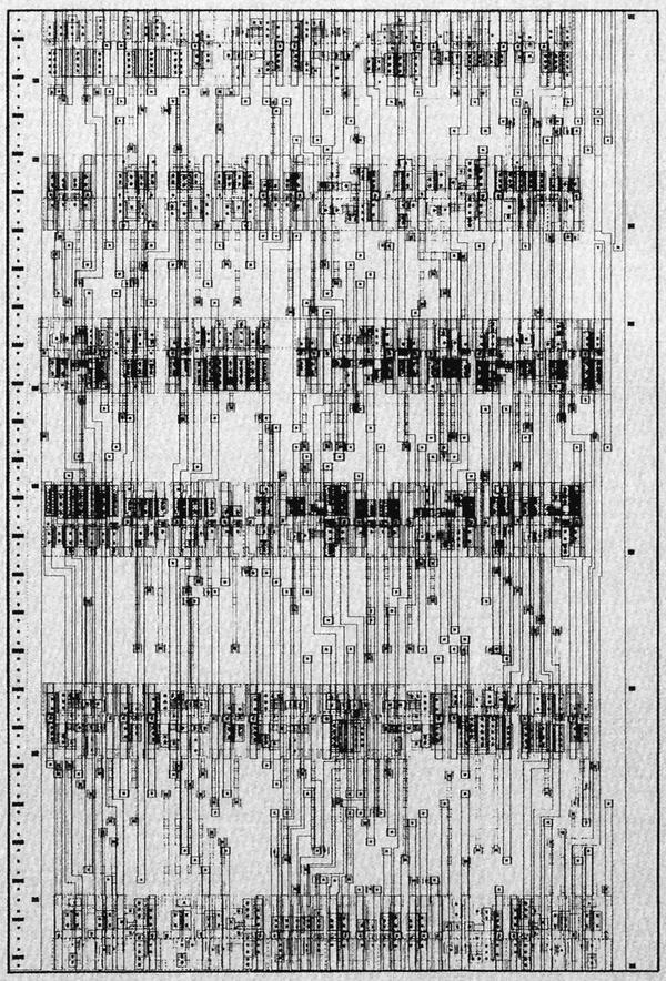
The APR386 paper discusses the standard-cell layout in detail. It includes a plot of a block of standard-cell circuitry (below).
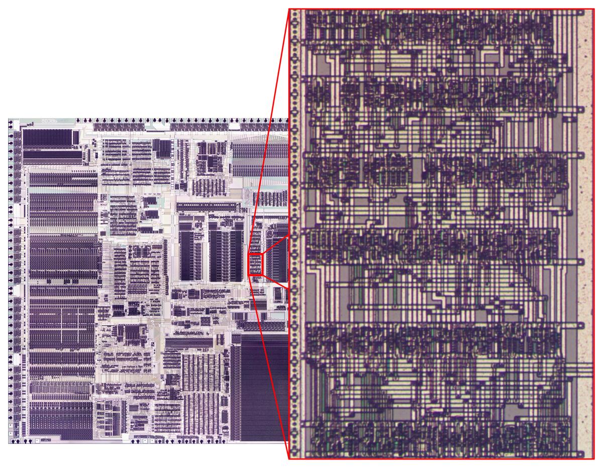
A block of standard-cell circuitry from APR386.After carefully studying the 386 die, I was able to find the location of this block of circuitry (below). The two regions match exactly; they look a bit different because the M1 metal layer (horizontal) doesn't show up in the plot above.
The same block of standard cells on the 386 die. -
Intel's CHMOS III standard cells are documented in Introduction to Intel Cell-Based Design (1988). The CHMOS IV library is discussed in Design Methodology for a 1.0µ Cell-based Library Efficiently Optimized for Speed and Area. The paper Validating an ASIC Standard Cell Library covers both libraries. ↩
-
For details on the 386's register file, see my earlier article. ↩
-
Source: "High Performance Technology Circuits and Packaging for the 80386", Jan Prak, Proceedings, ICCD Conference, Oct. 1986. ↩
-
I'll provide more history on standard cells in this footnote. RCA patented a bipolar standard cell in 1971, but this was a fixed arrangement of transistors and resistors, more of a gate array than a modern standard cell. Bell Labs researched standard cell layout techniques in the early 1970s, calling them Polycells, including a 1973 paper by Brian Kernighan. By 1979 A Guide to LSI Implementation discussed the standard cell approach and it was described as well-known in this patent application. Even so, Electronics called these design methods "futuristic" in 1980.
Standard cells became popular in the mid-1980s as faster computers and improved design software made it practical to produce semi-custom designs that used standard cells. Standard cells made it to the cover of Digital Design in August 1985, and the article inside described numerous vendors and products. Companies like Zymos and VLSI Technology (VTI) focused on standard cells. Traditional companies such as Texas Instruments, NCR, GE/RCA, Fairchild, Harris, ITT, and Thomson introduced lines of standard cell products in the mid-1980s. ↩


6 comments:
Thank you for the article. It brings back fun memories from nearly 30 years ago about working with the Magic layout tool and standard cells.
Is place & route as easy as NP-complete? That implies a polynomial-time way to verify that a given layout is optimal.
Ken,
A few minutes with Google will tell you that place and route is NP Complete for many restricted cases and NP Hard for unrestricted cases. But honestly, being able to verify a layout is optimal isn't the problem. The problem is finding an optimal layout in the first place.
The diagram “Simplified structure of the CMOS circuits” isn't right. I believe the substrates/body are the wrong type and the nmos/pmos labels are reversed.
Actually yes! I had the opportunity to work with skywater130nm tech in Magic. Indeed brings back memories!
This is so good; bridging CMOS Design with physical design for learners. Thanks a lot Ken!
Post a Comment