In 1979, Intel introduced the 8088 microprocessor, a variant of the 16-bit 8086 processor. IBM's decision to use the 8088 processor in the IBM PC (1981) was a critical point in computer history, leading to the dominance of the x86 architecture that continues to the present. One way that the 8086 and 8088 increased performance was by prefetching: the processor fetches instructions from memory before they are needed, so the processor can execute them without waiting on the relatively slow memory. I've been reverse-engineering the 8088 from die photos and this blog post discusses what I've uncovered about the prefetch circuitry.
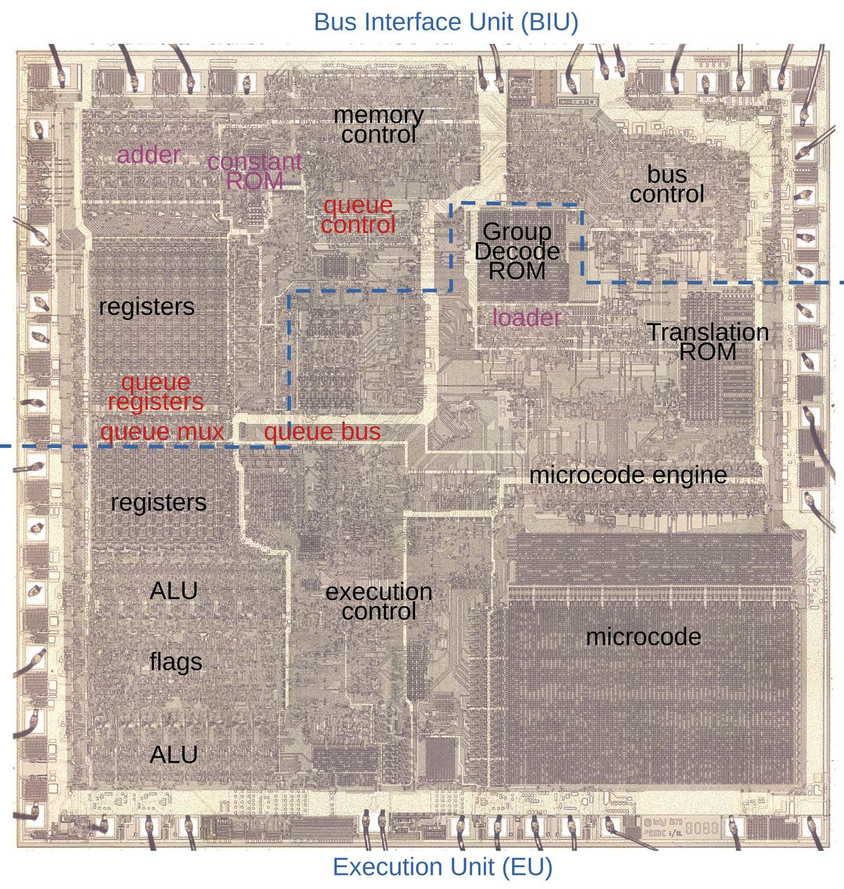
The die photo below shows the 8088 microprocessor under a microscope. The metal layer on top of the chip is visible, with the silicon and polysilicon mostly hidden underneath. Around the edges of the die, bond wires connect pads to the chip's 40 external pins. I've labeled the key functional blocks; this article focuses on the prefetch queue components highlighted in red. The components in purple also play a role, and will be discussed below. Architecturally, the chip is partitioned into a Bus Interface Unit (BIU) at the top and an Execution Unit (EU) below. The BIU handles memory accesses, while the Execution Unit (EU) executes instructions. In particular, the BIU fetches instructions, which are transferred from the prefetch queue to the Execution Unit via the queue bus.
The 8086 and 8088 processors present the same 16-bit architecture to the programmer. The key difference is that the 8088 has an 8-bit data bus for communication with memory and I/O, rather than the 16-bit bus of the 8086. The 8088's narrower bus reduced performance, since the processor only transfers one byte at a time rather than two. However, the 8-bit bus enabled cheaper computer hardware. The 8-bit bus was also a better match for hardware based on the older but popular 8-bit Intel 8080 and 8085 processors, allowing the reuse of 8-bit I/O circuitry for instance. Much of the IBM PC was based on the little-known IBM DataMaster, a computer built around the Intel 8085. Thus, selecting the 8088 processor was a natural choice for the IBM PC.
For the most part, the 8086 and 8088 are very similar internally, apart from trivial but numerous layout changes on the die. The biggest differences are in the Bus Interface Unit, the circuitry that communicates with memory and I/O devices, since this circuitry handles 16 bits in the 8086 versus 8 bits in the 8088. There are a few microcode differences between the two chips. One interesting change is that for performance reasons the 8088 has a smaller prefetch queue than the 8086 (four bytes instead of six). (I wrote about the 8086's prefetch circuity earlier.)
Prefetching and the architecture of the 8086 and 8088
The 8086 and 8088 were introduced at an interesting point in microprocessor history, when memory was becoming slower than the CPU. For the first microprocessors, the speed of the CPU and the speed of memory were comparable.2 However, as processors became faster, the speed of memory failed to keep up. The 8086 was probably the first microprocessor to prefetch instructions to improve performance. While modern microprocessors have megabytes of fast cache3 to act as a buffer between the CPU and much slower main memory, the 8088 has just 4 bytes of prefetch queue. However, this was enough to substantially increase performance.
Prefetching had a major impact on the design of the 8086 and thus the 8088. Earlier processors such as the 6502, 8080, or Z80 were deterministic: the processor fetched an instruction, executed the instruction, and so forth. Memory accesses corresponded directly to instruction fetching and execution and instructions took a predictable number of clock cycles. This all changed with the introduction of the prefetch queue. Memory operations became unlinked from instruction execution since prefetches happen as needed and when the memory bus is available.
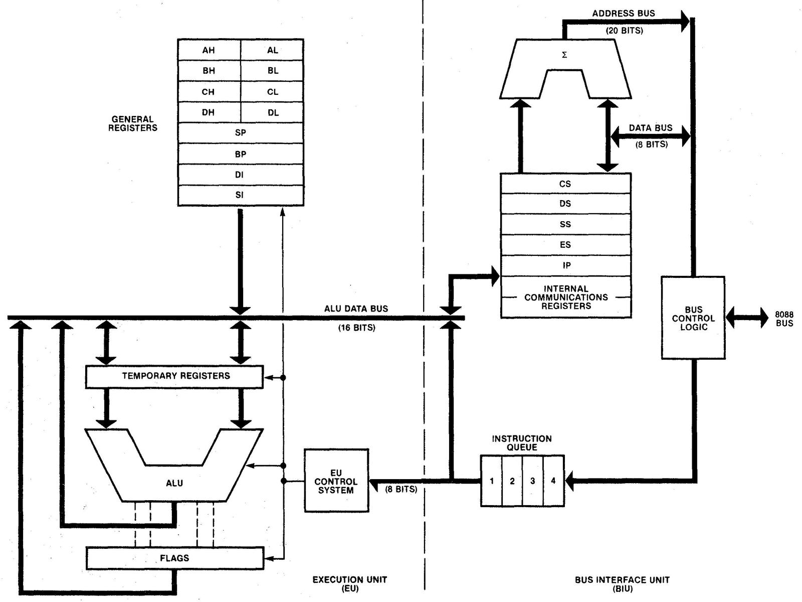
To handle memory operations and instruction execution independently, the implementors of the 8086 and 8088 divided the processors into two processing units: the Bus Interface Unit (BIU) that handles memory accesses, and the Execution Unit (EU) that executes instructions. The Bus Interface Unit contains the instruction prefetch queue; it supplies instructions to the Execution Unit via the Q (queue) bus. The BIU also contains an adder (Σ) for address calculation, adding the segment register base to an address offset, among other things. The Execution Unit is what comes to mind when you think of a processor: it has most of the registers, the arithmetic/logic unit (ALU), and the microcode that implements instructions. The segment registers (CS, DS, SS, ES) and the Instruction Pointer (IP) are in the Bus Interface Unit since they are directly involved in memory accesses, while the general-purpose registers are in the Execution Unit.
It may seem inefficient for the Bus Interface Unit to have its own adder instead of using the ALU, but there are reasons for the separate adder. First, every memory access uses the adder at least once to add the segment base and offset. The adder is also used to increment the PC or index registers. Since these operations are so frequent, they would create a bottleneck if they used the ALU. Second, since the Execution Unit and the Bus Interface Unit run asynchronously with respect to each other, it would be complicated to share the ALU without conflicts.
Prefetching had another major but little-known effect on the 8086 architecture: the designers were considering making the 8086 a two-chip microprocessor. Prefetching, however, required a one-chip design because the number of control signals required to synchronize prefetching across two chips exceeded the package pins available. This became a compelling argument for the one-chip design that was used for the 8086.4 (The unsuccessful Intel iAPX 432, which was under development at the same time, ended up being a two-chip processor: one to fetch and decode instructions, and one to execute them.)
Implementing the queue
The 8088's instruction prefetch queue is implemented with four 8-bit queue registers along with two hardware "pointers" into the queue. One two-bit counter keeps track of the current read position from 0 to 3, i.e. the queue register that will provide the next instruction byte. The second counter keeps track of the current write position, i.e. the queue register that will receive the next instruction from memory.5 As bytes are fetched from the queue, the read pointer advances. As bytes are added to the queue, the write pointer advances.
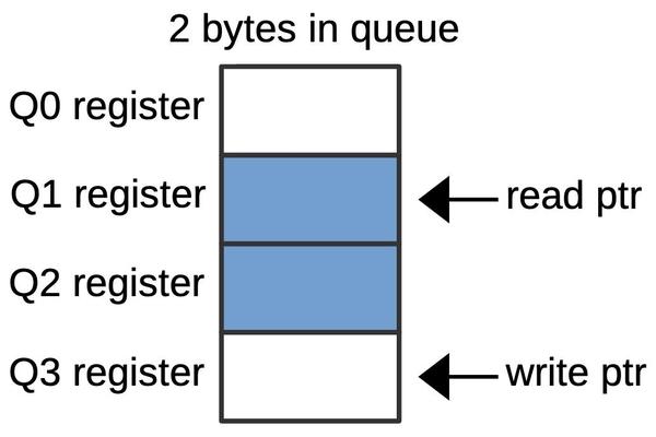
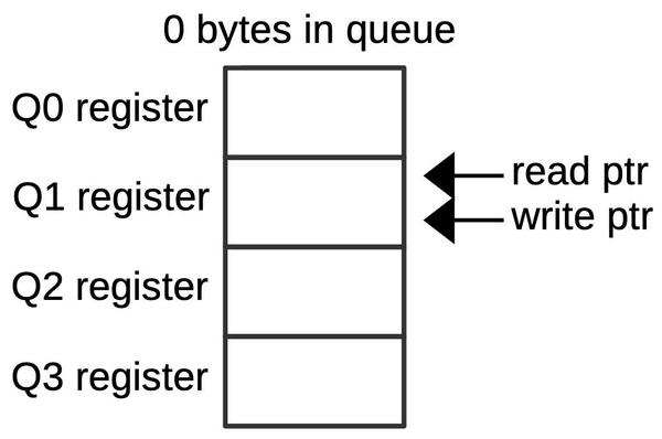
The diagram below shows an example queue configuration with two prefetched bytes. The middle two queue registers (Q1 and Q2) hold data. The read pointer indicates that the Execution Unit will get its next byte from Q1. The write pointer indicates that the next prefetched byte will go into Q3.
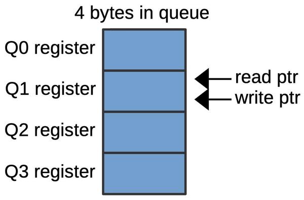
The diagram below shows how the queue pointers can wrap around. In this configuration, two more bytes have been written to the queue (Q3 and Q0), so the queue is full. The write pointer now points to Q1, the same as the read pointer.
There is an important ambiguity, however. Suppose that four bytes are read from the queue, so the read pointer advances four positions, wrapping around back to Q1. The queue is now empty, as shown below, but the pointers have the same position as the full case above. Thus, if the read pointer and the write pointer both point to the same position, the queue may be empty or full. To distinguish these cases, a flip-flop is set if the queue enters the empty state. This flip-flop generates a signal that Intel called MT (empty).
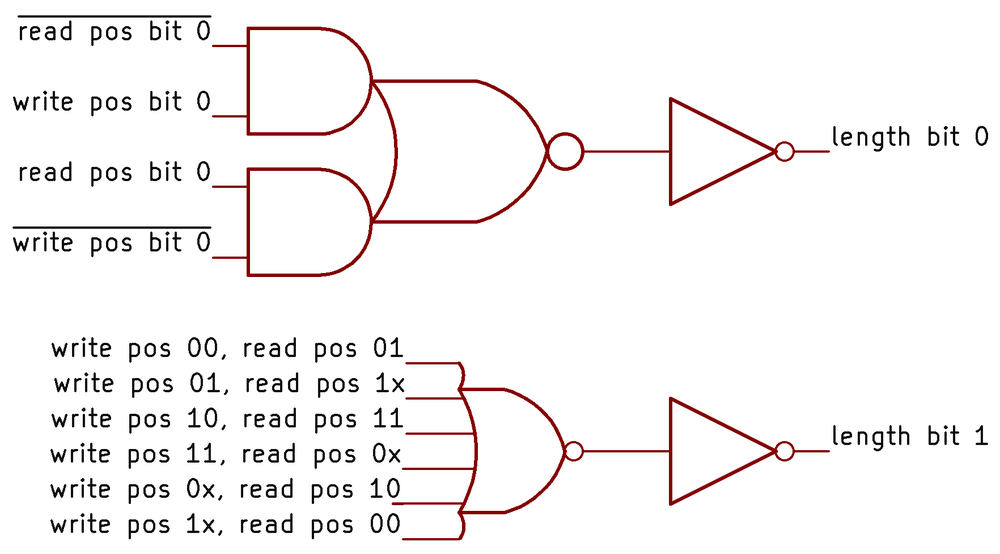
To determine how many bytes are in the queue, the queue circuitry uses a two-bit queue length value, along with the MT flip-flop value to distinguish the empty state. Conceptually, the queue length is generated by subtracting the read position from the write position. However, the implementation does not use a standard subtraction circuit, but instead uses hardcoded logic to determine the two bits of the length, as shown below.
The low bit of the length is the XOR of the two positions. In NMOS logic (used by the 8088), an AND-NOR gate is easy to implement, while an XOR gate is difficult. Thus, XOR is implemented as shown in the top circuit. (You can verify that if one input is 1 and the other is 0, the output is 1.) The high-order bit of the length is also based on an AND-NOR gate, one with six inputs. Each input is a combination of read and write positions that yields an output bit 1; each input is computed by a NOR gate, which I haven't drawn.6 As a result, the amount of logic circuitry to compute the length is fairly large.
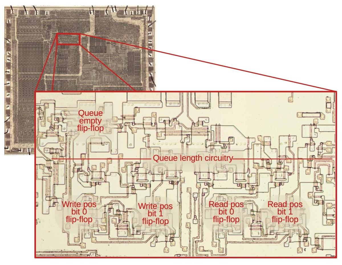
The diagram below zooms in on the queue control circuitry on the die, with the main flip-flops and circuitry labeled. The circuitry in the middle computes the queue length with the 6-input NOR gate stretched across the whole region. The flip-flops for the read and write positions are in the lower region. Despite the relative simplicity of the queue circuits, they take up a substantial part of the die. Compared to modern chips, the density of the 8088 is very low; you can almost see the flip-flops with the naked eye. But this isn't all the circuitry as prefetching also required queue registers and memory cycle control circuitry. Thus, prefetching was a moderately expensive feature for the 8088, as far as die area.
The loader
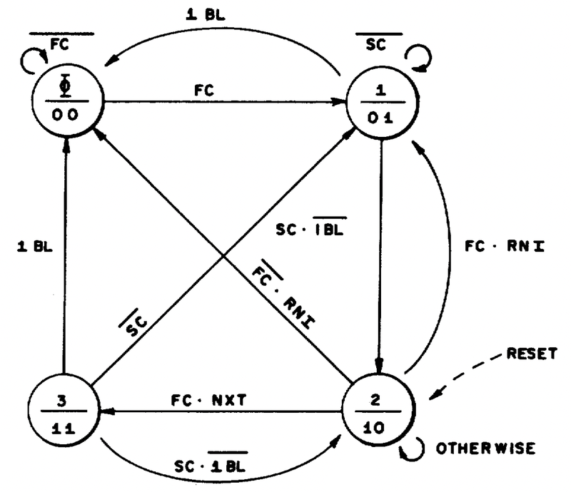
To decode and execute an instruction, the Execution Unit must get instruction bytes from the Bus Interface Unit, but this is not entirely straightforward. The main problem is that the queue can be empty, in which case instruction decoding must block until a byte is available from the queue. The second problem is that instruction decoding is relatively slow so it is pipelined. For maximum performance, the decoder needs a new byte before the current instruction is finished. A circuit called the "loader" solves these problems by providing synchronization between the prefetch queue and the instruction decoder. The loader uses a small state machine to efficiently fetch bytes from the queue at the right time and to provide timing signals to the decoder and microcode engine.
In more detail, as the loader requests the first two instruction bytes from the prefetch queue, it generates two timing signals that control the microcode execution. The FC (First Clock) indicates that the first instruction byte is available, while the SC (Second Clock) indicates the second instruction byte. Note that the First Clock and Second Clock are not necessarily consecutive clock cycles because the prefetch queue could be empty or contain just one byte, in which case the First Clock and/or Second Clock would be delayed. The instruction decoding circuitry and the microcode engine are controlled by the First Clock and Second Clock signals, so they remain synchronized with the bytes supplied by the prefetch queue.
At the end of a microcode sequence, the Run Next Instruction (RNI) micro-operation causes the loader to fetch the next machine instruction. However, fetching and decoding the next instruction is a bit slow so microcode execution would be blocked for a cycle. In many cases, this slowdown can be avoided: if the microcode knows that it is one micro-instruction away from finishing, it issues a Next-to-last (NXT) micro-operation so the loader can start loading the next instruction. This achieves a degree of pipelining in most cases; fetching the next instruction is overlapped with finishing the execution of the previous instruction.
The diagram above shows the state machine for the loader. I won't explain it in detail, but essentially it keeps track of whether it is waiting for a First Clock byte or a Second Clock byte, and if it is performing a fetch in advance (NXT) or at the end of an instruction (RNI). The state machine is implemented with two flip-flops to support its four states.
Microcode and the prefetch queue
The loader takes care of fetching an instruction that consists of an opcode byte and a Mod R/M (addressing mode) byte. However, many instructions have additional bytes or don't follow this format For example, an opcode such as "ADD AX" can be followed by an 8- or 16-bit immediate value, adding that value to the AX register. Or a "move memory to AX" instruction can be followed by a 16-bit memory address The microcode uses a separate mechanism for fetching these instruction bytes from the queue. Specifically, each micro-instruction contains a source register and a destination register that specify a data move. By specifying "Q" (the queue) as the source, a byte is fetched from the prefetch queue. If the queue is empty, microcode execution blocks until the Bus Interface Unit loads a byte into the prefetch queue. Thus, the complexity of instruction fetching and the prefetch queue is invisible to the microcode.7
A jump, subroutine call, or other control flow change causes the prefetch queue to be flushed since the queue contents
are no longer useful.
This is accomplished in microcode with the FLUSH micro-instruction, which resets the queue read and write pointers and
sets the MT (empty) flip-flop.
Note that the queue is flushed even if the target address is in the queue, for example if you jump one byte ahead.
One complication due to the prefetch queue is that the processor's Instruction Pointer points to the next instruction to
be fetched, not the next instruction to be executed.
This becomes a problem for a subroutine call, which needs to push the return address.
It is also a problem for a relative jump, which is computed from the current instruction.
The solution is the CORR micro-instruction, which corrects the Instruction Pointer by subtracting the queue length to
determine the current execution position.
This is implemented by the Bus Interface Unit, which holds correction constants in the Constant ROM, and subtracts them
using the address adder (not the ALU).8
The queue registers
The 8086 and 8088 partition the registers into upper registers (in the Bus Interface Unit) and lower registers (in the Execution Unit). The upper registers are the registers associated with memory accesses (e.g. Instruction Pointer, segment registers) while the lower registers are more general purpose (e.g. AX, BX, SI, SP). The upper registers are connected to two 16-bit internal buses: the B bus and the C bus.
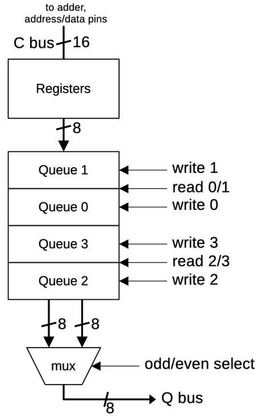
The queue registers are physically part of the upper registers, but are wired into the buses slightly differently, as shown below. In particular, the 8088's queue registers are written 8 bits at a time from the C bus. (In contrast, the 8086's queue registers can be written 16 bits at a time to support two-byte prefetches.) When accessing the queue, the queue registers are read 16 bits at a time, but only one byte is transferred to the Q bus for instruction processing.9
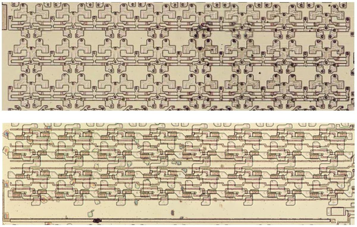
The diagram below shows how the queue registers appear on the die, comparing the six-byte prefetch queue in the 8086 (top) to the four-byte 8088 queue (bottom). The 8086 prefetch registers are structured as three rows of 16-bit registers, while the 8088 prefetch registers are structured as four rows of 8-bit registers. In both cases, each bit is stored in a cross-coupled pair of inverters. The bit lines (not present) are vertical, while the control lines to select a register are horizontal. The layout is different between the processors to support 16-bit versus 8-bit writes. Note the empty space at the bottom of the 8088 registers. Because the rest of the chips are mostly the same, the 8088 couldn't be "compacted" to avoid this wasted space.
Intel used simulations to determine the best queue sizes for the 8086 and 8088, balancing the performance cost of prefetching against the benefit. (The cost is that prefetching makes the bus unavailable for other memory or I/O operations.) The prefetch queue is discarded on a jump instruction or other change of control flow, causing the prefetched bytes to be wasted. Thus, as the queue gets longer, the chance of discarding a prefetched byte becomes larger, so the potential benefit of prefetching becomes smaller. Since the 8088 prefetches one byte at a time, compared to two bytes at a time on the 8086, prefetching on the 8088 costs twice as much as on the 8086 in terms of bus cycles used per byte. This changes the tradeoffs in favor of a shorter queue.
Because of the difference in queue lengths, the queue control circuitry is different between the 8086 and 8088. In particular, the 8086 needs three-bit counters for the read and write positions, while the 8088 uses two-bit counters. Because of this, the length computation circuitry is also different between the processors.
I plan to continue reverse-engineering the 8088 die so follow me on Twitter @kenshirriff or RSS for updates. I've also started experimenting with Mastodon recently as @oldbytes.space@kenshirriff. If you're interested in the 8086, I wrote about the 8086 die, its die shrink process and the 8086 registers earlier.
Notes and references
-
Steve Furber, co-creator of the ARM chip, mentions that "The first integrated CPUs were coincidentally quite well matched to semiconductor memory speeds, and were therefore built without caches. This can now be seen as a temporary aberration." See VLSI Risc Architecture and Organization p77. To make this concrete, the Apple II (1977) used a MOS 6502 processor running at about 1 megahertz while its 4116 DRAM chips could perform an access in 250 nanoseconds (4 times the clock speed). The 8088 processor ran at 5-10 MHz which meant that 250 ns DRAM chips were slower than the clock speed. Nowadays, processors run at 4 GHz but DRAM access speed is about 50 nanoseconds (1/200 the clock speed). ↩
-
Modern processors use caches to improve memory performance. Accessing data from a cache is faster than accessing it from main memory, but the tradeoff is that caches are much smaller than main memory. The prefetch queues in the 8086 and 8088 are similar to a cache in some ways, but there are some key differences. First, the prefetch queue is strictly sequential. If you jump ahead two bytes, even if the prefetch queue has those instruction bytes, the processor can't use them. Second, the prefetch queue can't reuse bytes. If you have a 6-byte loop, even though all the code fits in the prefetch queue, it will be reloaded every time. Third, the prefetch queue doesn't provide any consistency. If you modify an instruction in memory a couple of bytes ahead of the PC, the 8086 or 8088 will run the old instruction if it's in the queue. ↩
-
The design decisions for the 8086 prefetch cache (and many other aspects of the chip) are described in: J. McKevitt and J. Bayliss, "New options from big chips," in IEEE Spectrum, vol. 16, no. 3, pp. 28-34, March 1979, doi: 10.1109/MSPEC.1979.6367944. Prefetch provided a 50% performance benefit to the 8086. ↩
-
The queue read process doesn't use an explicit read operation. Instead, the selected queue register continuously puts its value onto the queue bus. When the Execution Unit uses this byte, it sends an increment signal to the queue to advance the read pointer. If the queue empty (MT) flip-flop is set, the Execution Unit will wait until a byte is ready. ↩
-
The NOR gates are used as AND gates, following DeMorgan's laws. For example to produce a 1 output for write position 00 and read position 01, the logic is:
NOR(write bit 1', write bit 0', read bit 1', read bit 0). Note that the bits into the NOR gate are all inverted from the "desired" values; if they are all 0, the NOR output is 1. Thus, there are also some inverters on the inputs. ↩ -
Arbitrary memory reads and writes are performed directly on memory, bypassing the prefetch queue. The 8086/8088 do not provide consistency; if you modify an instruction byte in memory and the byte is in the queue, the processor will execute the old byte. (This type of self-modifying code can be used to determine the queue length, distinguishing the 8086 from the 8088 in software.) ↩
-
The Constant ROM is used for more than just address correction. For example, it is also used to increment the Instruction Pointer after a prefetch. Other constants are used for the 8088's string operations, which act on a block of memory. The index registers are incremented or decremented by 1 for bytes or 2 for words. When popping a value from the stack, the stack pointer is decremented using the Constant ROM. ↩
-
Are the 8088's queue registers 16 bits wide or 8 bits wide? It's ambiguous, since the registers are written 8 bits at a time, but read 16 bits at a time. This implementation was probably selected to support the 8088's 8-bit bus while reusing as much of the 8086 design as possible. In particular, the 8088 can only prefetch one byte at a time, so writes need to happen a byte at a time. Thus, there are four control lines selecting which queue byte is written. (The 8088 could write to half of a 16-bit register but that would require moving the prefetched byte to the correct half of a 16-bit bus.) On the read side, it would make sense to have four read lines, selecting one byte from the 8088's queue. However, since the 8086 already had a multiplexer to select one byte from two, the 8088 designers probably felt it was easier to keep that circuit. And with the smaller queue on the 8088, there was no need to try to save space by removing the circuit. Thus, the queue has two read-select lines and a multiplexer control line. All these lines are controlled by the write position and read position flip-flops. ↩
11 comments:
Self-modifying code was relatively common in the early days of the IBM PC, and sometimes it would rely on the fact that a jump would discard the prefetch queue, to ensure that the CPU executed a modified instruction. Because of this, current versions of the x86 still guarantee that self-modified code will be visible to the CPU's execution pipeline immediately after any branch -- see section 8.1.3 of volume 3A of the "Intel(R) 64 and IA-32 Architectures Software Developer's Manual".
Equally some copy protection schemes would write into the prefetch queue (just ahead of the PC) so that if you were single stepping you would branch somewhere off into the weeds
What's the purpose of this, it's an archeology with little usability?
Anonymous: yes :-)
It's of great utility value to people like me, who are interested to know just what was going through the minds of the people who designed this wacky architecture :)
It's great to see a quote from Steve Furber! I hate to question part of the premise at the beginning of the blog post, but I understood that the prefetch queue on the 8086 and 8088 existed because the CPU was often slower than RAM, and in this way, differs from a cache (where RAM is slower than the CPU).
Firstly, when I think about DRAM accesses, as Steve Furber says, even 1977's 250ns RAM would match quite well with the 8086/8088, because it took 4 cycles to fetch a byte or word. I understand that the address is valid at T1.5, and data is read at T(3+n).5 where n is the number of wait states. This means an original 5MHz 8086 needs 400ns or faster RAM doesn't it?
However, the Execution unit, can of course sometimes process instructions faster than the bus can read them: at up to 2 or 3 cycles per instruction vs 4 cycles per bus fetch. But when the EU is doing that, it becomes bus & memory speed limited, so the prefetch queue doesn't help. Instead, the execution rate slows down to the bus bandwidth (a long sequence of 2 or 3 cycle ALU operations). And on an 8088 that's 8 cycles per 2 byte ALU operation (pretty much everything apart from inc/dec).
Thirdly, a cache helps primarily with the principle of locality, but the BIU doesn't. For example, a loop small enough to fit in the 8086's queue, e.g.
lp: add al,[SI]
inc si
loop lp
Forces a BIU flush. Even rep movsw will force prefetch queue reloads simply by observing the 20-odd cycles needed per loop (and the fact that it can be interrupted). That's different to the 68010 whose similar length 3 x 16-bit word cache is specifically designed to speed up move.w (as)+,(ad)+ dbra dn,lp type loops.
Surely, what the prefetch queue helps with is when the CPU is slower than the memory and the bus timing, i.e. when it has internal cycles, e.g. MUL/DIV or shift,cl or an EA calculation (BX+SI); then the bus can fetch future instructions during the calculation, and even a fairly simple EA is enough to fetch a couple of 16-bit words before it's ready to perform the memory fetch/store.
The real question for me is why is the 8088 faster with a 4-byte queue rather than a 6-byte queue as on the earlier 8086? As you say, it's because the prefetch queue soaks up bandwidth so when there's a change in the control flow, the BIU could have wasted cycles delaying some prior data memory requests, if they had been made after an instruction fetch had started.
But isn't another reason due to instruction alignment? The 8086 has a 16-bit bus, so sometimes a 6-byte queue is only as good as a 4-byte queue if you load a pair of instructions that are misaligned (the first and last bytes get discarded) and most instructions are about 2 bytes (reg ALU, simple load/stores or short jumps). And 50% of the time that will be the case. Couldn't it be argued that the 8086 needs a 6-byte queue to achieve what the 8088 can do with 4 bytes and those 6 bytes are the limit of the liability of the BIU (which could explain why even though bus cycles are faster, the 80188 queue remains at 4 bytes, while the 80186 and 80286 queues remain at 6 bytes and why the '386 queue is 12 bytes... after the bug fix. This makes sense if we assume the RAM could already keep up, and the prefetch queue exists to soak up internal cycles.).
Since the 8088 and 8086 post-queue logic appears to be essentially the same, once the queue is MT, does the 8088 have to wait for all 16 bits to be pre-fetched before the first byte can be drawn from the queue? If so, a sequence of instructions such as XCHG AX,BX, INC CX might take 4+4+3+2 clocks. If the first byte could be drawn from the queue immediately after it was fetched, the delay might be 4+4+2 with the execution time of the XCHG AX,BX being overlapped by the second fetch.
Hypothetically speaking:
How feasible would it be to reimplement this design, 100% logic gate level in a big enough FPGA? I'm not talking about re-designing, faking the output or whatever, i mean 100% logic gate level of accuracy?
Hola donde puedo encontrar el esquema interno del 8088
Hola me gustaría saber cómo tener el esquematico interno del 8088 tu lo tienes
Merci 👍
Post a Comment