Ferroelectric memory (FRAM) is an interesting storage technique that stores bits in a special "ferroelectric" material. Ferroelectric memory is nonvolatile like flash memory, able to hold its data for decades. But, unlike flash, ferroelectric memory can write data rapidly. Moreover, FRAM is much more durable than flash and can be be written trillions of times. With these advantages, you might wonder why FRAM isn't more popular. The problem is that FRAM is much more expensive than flash, so it is only used in niche applications.
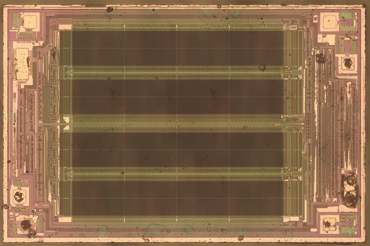
This post takes a look inside an FRAM chip from 1999, designed by a company called Ramtron. The die photo above shows this 64-kilobit chip under a microscope; the four large dark stripes are the memory cells, containing tiny cubes of ferroelectric material. The horizontal greenish bands are the drivers to select a column of memory, while the vertical greenish band at the right holds the sense amplifiers that amplify the tiny signals from the memory cells. The eight whitish squares around the border of the die are the bond pads, which are connected to the chip's eight pins.1 The logic circuitry at the left and right of the die implements the serial (I2C) interface for communication with the chip.2
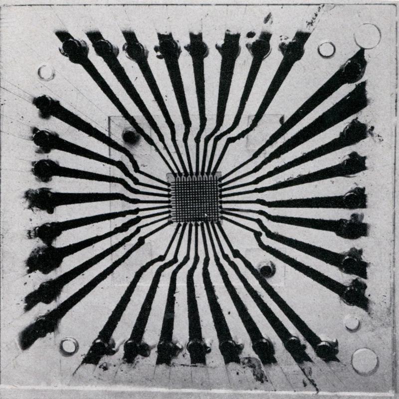
The history of ferroelectric memory dates back to the early 1950s.3 Many companies worked on FRAM from the 1950s to the 1970s, including Bell Labs, IBM, RCA, and Ford. The 1955 photo below shows a 256-bit ferroelectric memory built by Bell Labs. Unfortunately, ferroelectric memory had many problems,4 limiting it to specialized applications, and development was mostly abandoned by the 1970s.
Ferroelectric memory had a second chance, though. A major proponent of ferroelectric memory was George Rohrer, who started working on ferroelectric memory in 1968. He formed a memory company, Technovation, which was unsuccessful, and then cofounded Ramtron in 1984.5 Ramtron produced a tiny 256-bit memory chip in 1988, followed by much larger memories in the 1990s.
How FRAM works
Ferroelectric memory uses a special material with the property of ferroelectricity. In a normal capacitor, applying an electric field causes the positive and negative charges to separate in the dielectric material, making it polarized. However, ferroelectric materials are special because they will retain this polarization even when the electric field is removed. By polarizing a ferroelectric material positively or negatively, a bit of data can be stored. (The name "ferroelectric" is in analogy to "ferromagnetic", even though ferroelectric materials are not ferrous.)
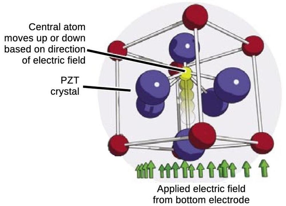
This FRAM chip uses a ferroelectric material called lead zirconate titanate or PZT, containing lead, zirconium, titanium, and oxygen. The diagram below shows how an applied electric field causes the titanium or zirconium atom to physically move inside the crystal lattice, causing the ferroelectric effect. (Red atoms are lead, purple are oxygen, and yellow are zirconium or titanium.) Because the atoms physically change position, the polarization is stable for decades; in contrast, the capacitors in a DRAM chip lose their data in milliseconds unless refreshed. FRAM memory will eventually wear out, but it can be written trillions of times, much more than flash or EEPROM memory.
To store data, FRAM uses ferroelectric capacitors, capacitors with a ferroelectric material as the dielectric between the plates. Applying a voltage to the capacitor will create an electric field, polarizing the ferroelectric material. A positive voltage will store a 1, and a negative voltage will store a 0.
Reading a bit from memory is a bit tricky. A positive voltage is applied, forcing the material into the 1 state. If the material was already in the 1 state, minimal current will flow. But if the material was in the 0 state, more current will flow as the capacitor changes state. This allows the 0 and 1 states to be distinguished.
Note that reading the bit destroys the stored value. Thus, after a read, the 0 or 1 value must be written back to the capacitor to restore its previous state. (This is very similar to the magnetic core memory that was used in the 1960s.)6
The FRAM chip that I examined uses two capacitors per bit, storing opposite values. This approach makes it easier to distinguish a 1 from a 0: a sense amplifier compares the two tiny signals and generates a 1 or a 0 depending on which is larger. The downside of this approach is that using two capacitors per bit reduces the memory capacity. Later FRAMs increased the density by using one capacitor per bit, along with reference cells for comparison.7
A closer look at the die
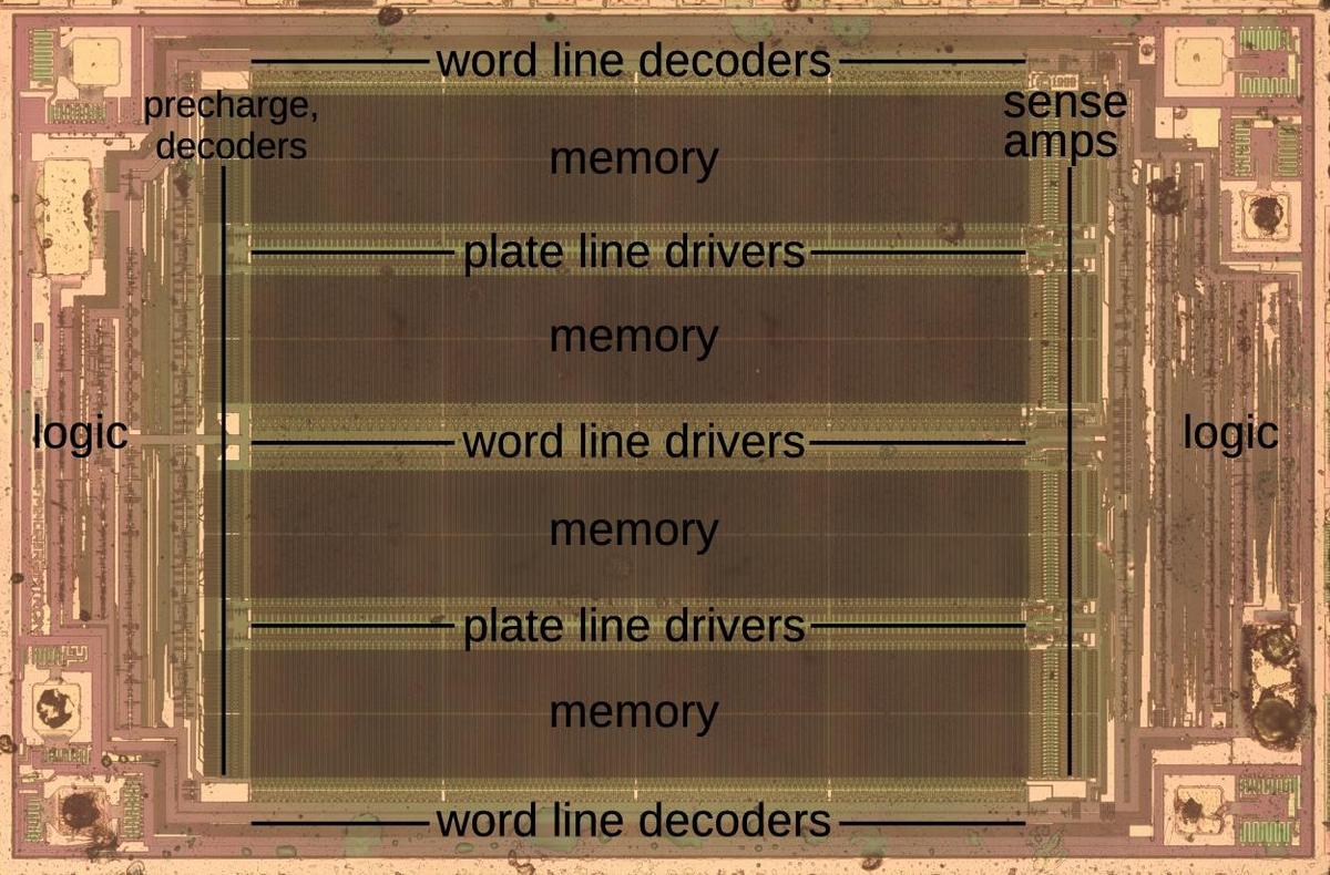
The diagram below shows the main functional blocks of the chip.8 The memory itself is partitioned into four blocks. The word line decoders select the appropriate column for the address and the drivers generate the pulses on the word and plate lines. The signals from that column go to the sense amplifiers on the right, where the signals are converted to bits and written back to memory. On the left, the precharge circuitry charges the bit lines to a fixed voltage at the start of the memory cycle, while the decoders select the desired byte from the bit lines.
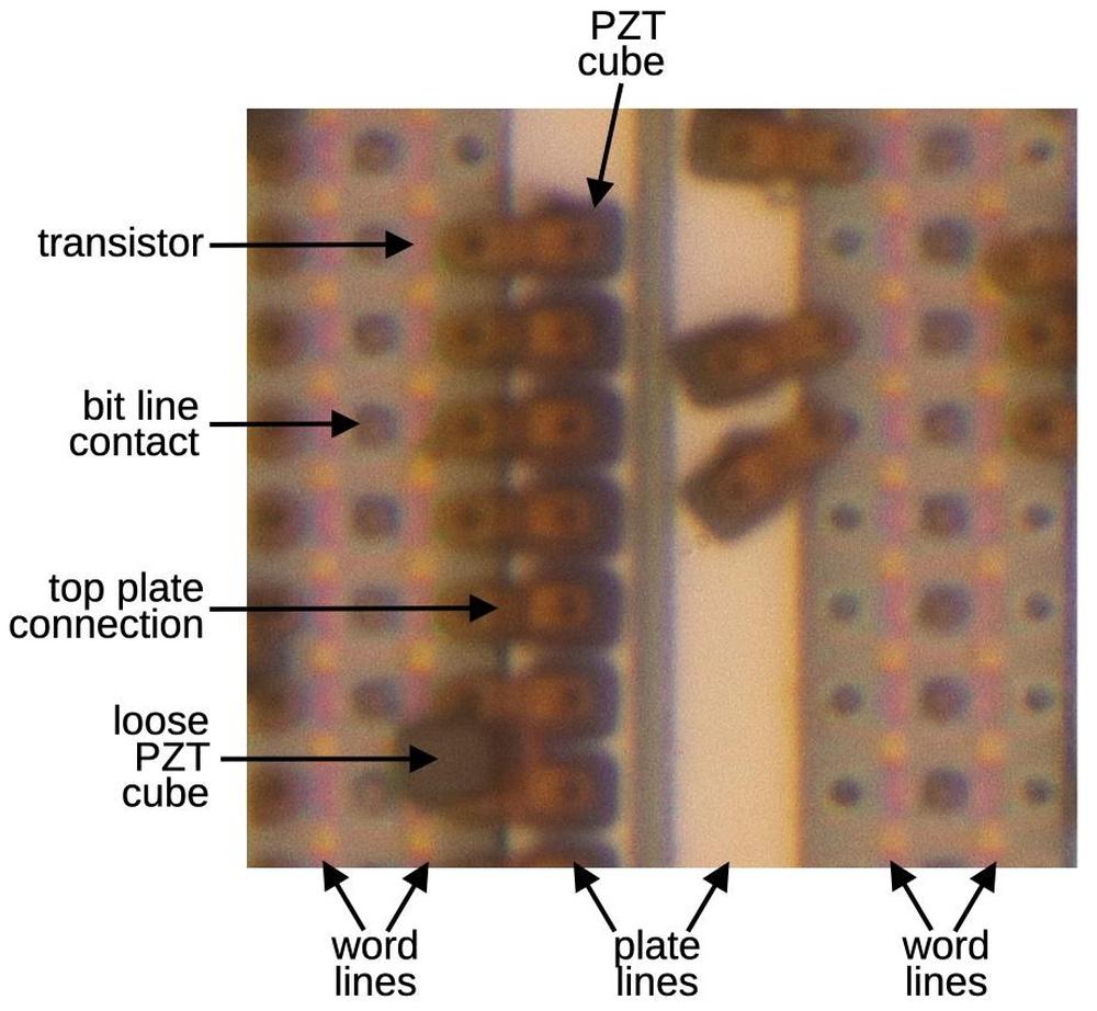
The diagram below shows a closeup of the memory. I removed the top metal layer and many of the memory cells to reveal the underlying structure. The structure is very three-dimensional compared to regular chips; the gray squares in the image are cubes of PZT, sitting on top of the plate lines. The brown rectangles labeled "top plate connection" are also three-dimensional; they are S-shaped brackets with the low end attached to the silicon and the high end contacting the top of the PZT cube. Thus, each PZT cube forms a capacitor with the plate line forming the bottom plate of the capacitor, the bracket forming the top plate connection, and the PZT cube sandwiched in between, providing the ferroelectric dielectric. (Some cubes have been knocked loose in this photo and are sitting at an angle; the cubes form a regular grid in the original chip.)
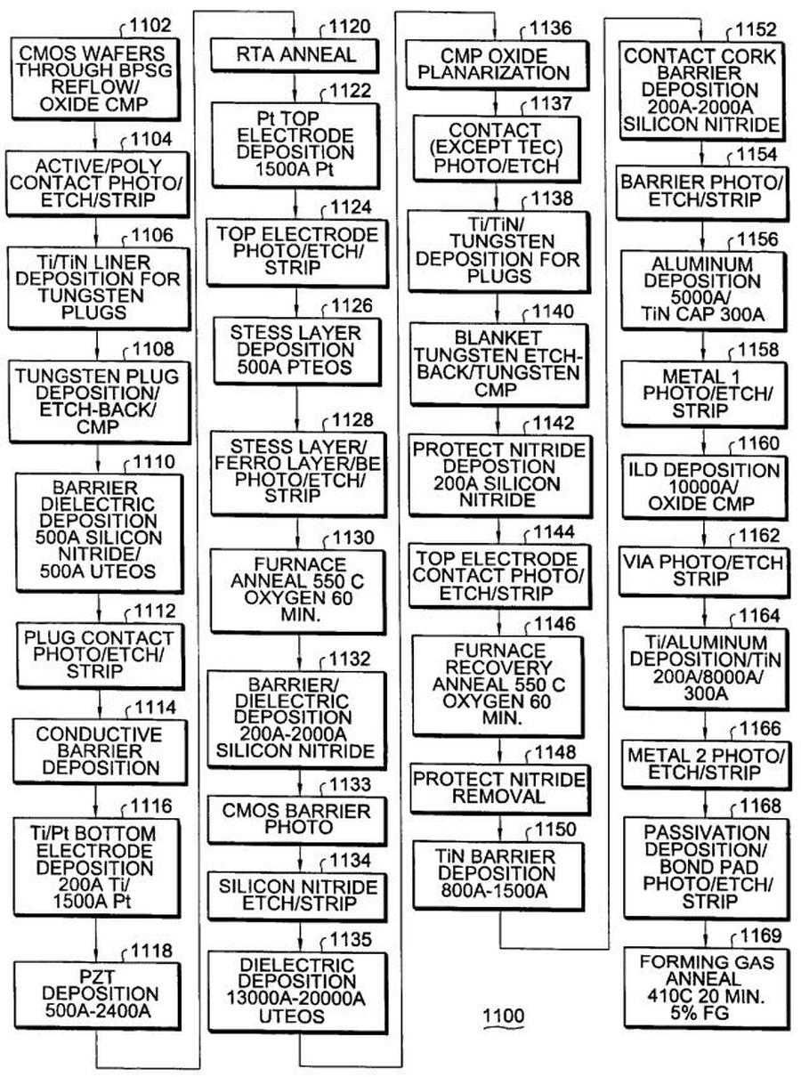
The physical design of the chip is complicated and quite different from a typical planar integrated circuit. Each capacitor requires a cube of PZT sandwiched between platinum electrodes, with the three-dimensional contact from the top of the capacitor to the silicon. Creating these structures requires numerous steps that aren't used in normal integrated circuit fabrication. (See the footnote9 for details.) Moreover, the metal ions in the PZT material can contaminate the silicon production facility unless great care is taken, such as using a separate facility to apply the ferroelectric layer and all subsequent steps.10 The additional fabrication steps and unusual materials significantly increase the cost of manufacturing FRAM.
Each top plate connection has an associated transistor, gated by a vertical word line.11 The transistors are connected to horizontal bit lines, metal lines that were removed for this photo. A memory cell, containing two capacitors, measures about 4.2 µm × 6.5 µm. The PZT cubes are spaced about 2.1 µm apart. The transistor gate length is roughly 700 nm. The 700 nm node was introduced in 1993, while the die contains a 1999 copyright date, so the chip appears to be a few years behind the cutting edge as far as node.
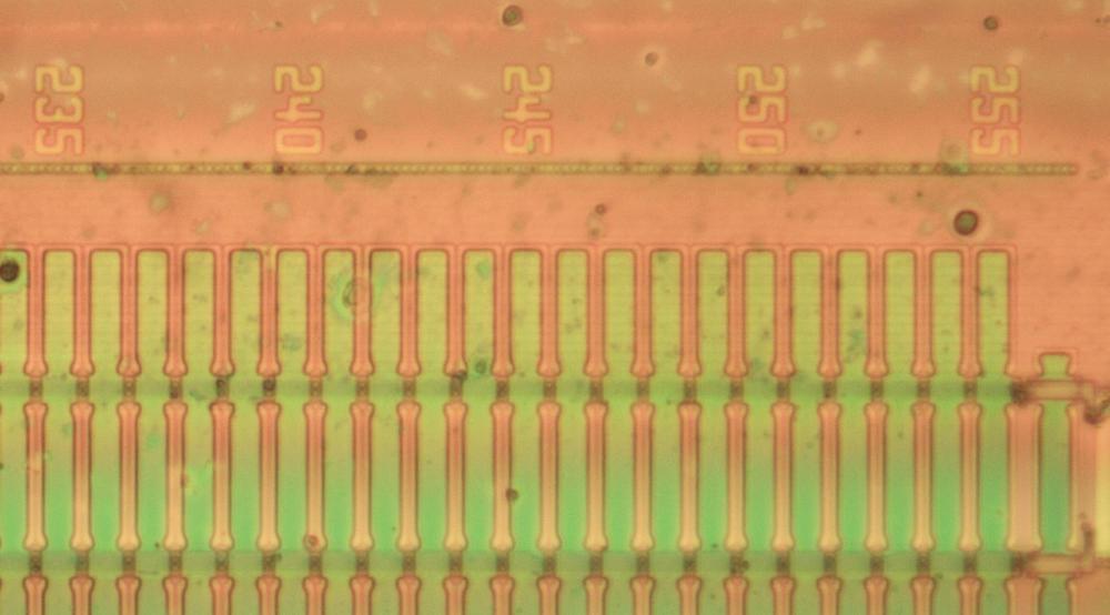
The memory is organized as 256 capacitors horizontally by 512 capacitors vertically, for a total of 64 kilobits (since each bit requires two capacitors). The memory is accessed as 8192 bytes. Curiously, the columns are numbered on the die, as shown below.
The photo below shows the sense amplifiers to the right of the memory, with some large transistors to boost the signal. Each sense amplifier receives two signals from the pair of capacitors holding a bit. The sense amplifier determines which signal is larger, deciding if the bit is a 0 or 1. Because the signals are very small, the sense amplifier must be very sensitive. The amplifier has two cross-connected transistors with each transistor trying to pull the other signal low. The signal that starts off larger will "win", creating a solid 0 or 1 signal. This value is rewritten to memory to restore the value, since reading the value erases the cells. In the photo, a few of the ferroelectric capacitors are visible at the far left. Part of the lower metal layer has come loose, causing the randomly strewn brown rectangles.
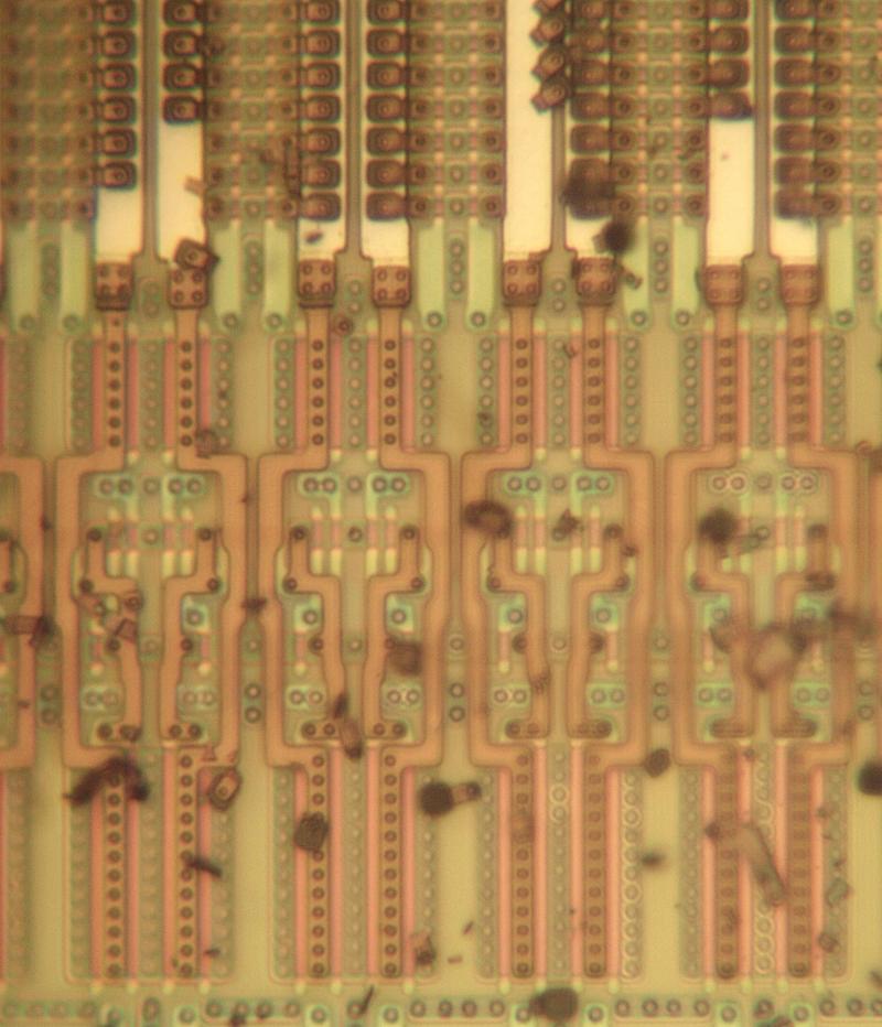
The photo below shows eight of the plate drivers, below the memory cells. This circuit generates the pulse on the selected plate line. The plate lines are the thick white lines at the top of the image; they are platinum so they appear brighter in the photo than the other metal lines. Most of the capacitors are still present on the plate lines, but some capacitors have come loose and are scattered on the rest of the circuitry. Each plate line is connected to a metal line (brown), which connects the plate line to the drive transistors in the middle and bottom of the image. These transistors pull the appropriate plate line high or low as necessary. The columns of small black circles are connections between the metal line and the silicon of the transistor underneath.
Finally, here's the part number and Ramtron logo on the die.
Conclusions
Ferroelectric RAM is an example of a technology with many advantages that never achieved the hoped-for success. Many companies worked on FRAM from the 1950s to the 1970s but gave up on it. Ramtron tried again and produced products but they were not profitable. Ramtron had hoped that the density and cost of FRAM would be competitive with DRAM, but unfortunately that didn't pan out. Ramtron was acquired by Cypress Semiconductor in 2012 and then Cypress was acquired by Infineon in 2019. Infineon still sells FRAM, but it is a niche product, for instance satellites that need radiation hardness. Currently, FRAM costs roughly $3/megabit, almost three orders of magnitude more expensive than flash memory, which is about $15/gigabit. Nonetheless, FRAM is a fascinating technology and the structures inside the chip are very interesting.
For more, follow me on Mastodon as @[email protected] or RSS. (I've given up on Twitter.) Thanks to CuriousMarc for providing the chip, which was used in a digital readout (DRO) for his CNC machine.
Notes and references
-
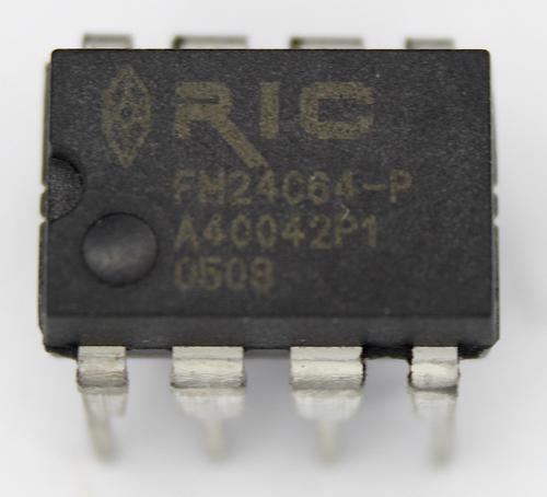
The photo below shows the chip's 8-pin package.
The chip is packaged in an 8-pin DIP. "RIC" stands for Ramtron International Corporation. -
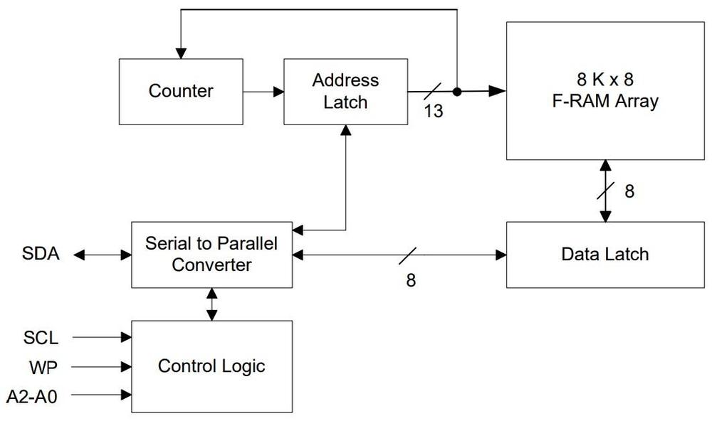
The block diagram shows the structure of the chip, which is significantly different from a standard DRAM chip. The chip has logic to handle the I2C protocol, a serial protocol that uses a clock and a data line. (Note that the address lines A0-A2 are the address of the chip, not the memory address.) The WP (Write Protect) pin, protects one quarter of the chip from being modified. The chip allows an arbitrary number of bytes to be read or written sequentially in one operation. This is implemented by the counter and address latch.
Block diagram of the FRAM chip. From the datasheet. -
An early description of ferroelectric memory is in the October 1953 Proceedings of the IRE. This issue focused on computers and had an article on computer memory systems by J. P. Eckert of ENIAC fame. In 1953, computer memory systems were primitive: mercury delay lines, electrostatic CRTs (Williams tubes), or rotating drums. The article describes experimental memory technologies including ferroelectric memory, magnetic core memory, neon-capacitor memory, phosphor drums, temperature-sensitive pigments, corona discharge, or electrolytic diodes. Within a couple of years, magnetic core memory became successful, dominating storage until semiconductor memory took over in the 1970s, and most of the other technologies were forgotten. ↩
-
A 1969 article in Electronics discussed ferroelectric memories. At the time, ferroelectric memories were used for a few specialized applications. However, ferroelectric memories had many issues: slow write speed, high voltages (75 to 150 volts), and expensive logic to decode addresses. The article stated: "These considerations make the future of ferroelectric memories in computers rather bleak." ↩
-
Interestingly, the "Ram" in Ramtron comes from the initials of the cofounders: Rohrer, Araujo, and McMillan. Rohrer originally focused on potassium nitrate as the ferroelectric material, as described in his patent. (I find it surprising that potassium nitrate is ferroelectric since it seems like such a simple, non-exotic chemical.) An extensive history of Ramtron is here. A Popular Science article also provides information. ↩
-
Like core memory, ferroelectric memory is based on a hysteresis loop. Because of the hysteresis loop, the material has two stable states, storing a 0 or 1. While core memory has a hysteresis loop for magnetization with respect to the magnetic field, ferroelectric memory The difference is that core memory has hysteresis of the magnetization with respect to the applied magnetic field, while ferroelectric memory has hysteresis of the polarization with respect to the applied electric field. ↩
-
The reference cell approach is described in Ramtron patent 6028783A. The idea is to have a row of reference capacitors, but the reference capacitors are sized to generate a current midway between the 0 current and the 1 current. The reference capacitors provide the second input to the sense amplifiers, allowing the 0 and 1 bits to be distinguished. ↩
-
Ramtron's 1987 patent describes the approximate structure of the memory. ↩
-
The diagram below shows the complex process that Ramtron used to create an FRAM chip. (These steps are from a 2003 patent, so they may differ from the steps for the chip I examined.)
Ramtron's process flow to create an FRAM die. From Patent 6613586.Abbreviations: BPSG is borophosphosilicate glass. UTEOS is undoped tetraethylorthosilicate, a liquid used to deposit silicon dioxide on the surface. RTA is rapid thermal anneal. PTEOS is phosphorus-doped tetraethylorthosilicate, used to create a phosphorus-doped silicon dioxide layer. CMP is chemical mechanical planarization, polishing the die surface to be flat. TEC is the top electrode contact. ILD is interlevel dielectric, the insulating layer between conducting layers. ↩
-
See the detailed article Ferroelectric Memories, Science, 1989, by Scott and Araujo (who is the "A" in "Ramtron"). ↩
-
Early FRAM memories used an X-Y grid of wires without transistors. Although much simpler, this approach had the problem that current could flow through unwanted capacitors via "sneak" paths, causing noise in the signals and potentially corrupting data. High-density integrated circuits, however, made it practical to associate a transistor with each cell in modern FRAM chips. ↩


16 comments:
Hmm. Ferroelectric memory would be perfect in high-radiation environments, such as nuclear energy or spaceflight.
My former company had an ARM based reference design that offered a Ramtron FRAM memory module on it for development purposes. Same 8KiB capacity, it was just another device on the I2C bus you could use for data storage that didn't wear out. It was a surface mount part, and I'm not really sure why we included it - other than as an infinite write non volatile memory device. There was also a regular I2C EEPROM on the board. I never expected those FRAM devices to ever fail.
Even in rad hard applications FRAM has been supplanted by MRAM. Or at least it has been for aerospace.
I've found FRAM chips in photocopiers and other interesting places. I've designed it into several embedded products since it has a practically infinite cycle life and has no need for a flash translation layer or wear leveling. This provides constant access time performance and reduced code complexity. It also allows the system state to be written constantly and handle power loss beautifully. These systems also had NOR flash for large storage, like firmware. I also support using FRAM for low-volume or hobby projects where the engineering effort saved by using a hardcoded memory map outweighs the chip cost. One thing I've never used, but is quite interesting, is the MSP430 TI produced with the internal SRAM replaced with FRAM. This allowed the chip to enter effectively a shutdown state and resume without losing any memory or register contents.
I implemented a triple micro controllers
sharing 2 of 64mX8 (= 64meg x16) parallel Ramtron memory. Nothing else was fast enough, non volatile and I needed very fast (nanosecond) 16 bit real time access. Other static ram needed power, flash was well too slow & dram was a joke. Now Dram is fast enough, but flash is still relatively slow.
I suspect massive dram production killed fram because production could never ramp up to the numbers needed to make it viable both in delivery time & cost.
What fram is suited for is very fast low power (battery) data gathering. No need to do anything with the raw data it is stored!
Something has gone wrong in footnote 6. Maybe a pasting error?
Ramtron make the FM1806 which is a byte-wide 32 KiByte part with a 70 ns access time. Timing, control signals, and pinout make it a viable replacement for regular SRAMs. It can be used for making 8-bit retro systems that can re-write themselves without special software (effectively making the device a mix of RAM and ROM on a byte level without having to have two devices and decoding).
One FRAM application that many people encountered without knowing it is in the game cartridge of Sonic the Hedgehog 3 for the Sega Megadrive (Sega Genesis in the US). The console itself provided no ability to save the progress of a game, so each cartridge had to implement this itself. I think Sonic 3 was unique in using FRAM (Ramtron FM1208S) -- all other cartridges used either SRAM with a coin cell battery or (later) serial EPROM. With four million copies sold, presumably Sega got a good deal on the chips.
With a microscope like that you've gotta take a look at Optane PRAM by Intel.
The worst thing about a FRAM chip is you have to change the oil filter every 5,000 miles.
FRAM technology isn't completely dead; TI still uses it as a replacement for Flash on some of their MSP430 family chips. It'd be interesting to see how different their version of it is from the original
You say that flash is $15/gigabit. That makes me wonder whether you mean $15/terabit, or whether the "flash" thumb drives that are sold at prices commensurate with the latter costing are a different technology from what you are talking about....?
Actually, Texas Instruments provides the MSP430 mpu that includes ferroram instead of flash, for program storage. https://en.wikipedia.org/wiki/TI_MSP430
Intel Optane technically use a version of FRAM - and it's honestly not as reliable as you think especially at node smaller than 40 nanometers, partly why they abandoned Optane and the fact that Infineon still struggles to expand FRAMs over 32 megabytes. FRAM however is excellent for lower power data logging with microcontrollers writing to it repeatedly, and not to mention some game cartridges.
Lastly, MRAM is starting to replace FRAM completely for reliability reasons (it easily outlasts FRAM in term of rewrite endurance and doesn't have false write problems that FRAMs still suffer from), not to mention much cheaper to make.
That's something I'm playing with. I found some DIP packaged ones and had the idea to breadboard a CPU, Ben Eater style, using the FRAM as both RAM and ROM with some simple logic to keep the CPU from writing the ROM block. Much quicker to reprogram than a PROM, and saves a chip.
They're interesting chips, with very low power usage. I wrote some code for one that uses a chunk of the FRAM as (non volatile) RAM (this is supported), so it can carry state through a total power outage. The efficiency of some of these chips is amazing: wearable glucose monitors use the RF430 which can either be powered by NFC or a tiny 7mm button cell with a capacity of 1.55V @ 24mAH for two weeks.
Post a Comment