On the surface, a microprocessor's registers seem like simple storage, but not in the 8085 microprocessor.
Reverse-engineering the 8085 reveals many interesting tricks that make the registers fast and compact.
The picture below shows that the registers and associated control circuitry occupy a large fraction of the chip, so efficiency is important. Each bit is implemented with a surprisingly compact circuit.
The instruction set is designed to make register accesses efficient.
An indirection trick allows quick register exchanges. Many register operations use the unexpected but efficient data path of going through the ALU.
While the 8085's register complement is tiny compared to current processors, it has a solid register set by 1977 standards - about twice as many registers as the 6502. The 8085 has a 16-bit program counter, a 16-bit stack pointer, 16-bit BC, DE, and HL register pairs, and the 8-bit accumulator. The 8085 also has little-known hidden registers that are invisible to the programmer but used internally: the WZ register pair, and two 8-bit registers for the ALU: ACT and TMP.

Photograph of the 8085 chip showing components relevant to register operations.
The register file is in the lower left quadrant of the chip. It contains the 6 register pairs and associated circuitry. Underneath the registers is the 16-bit address latch and increment/decrement circuit. The register file is controlled by a set of control lines on the right, which are driven by register control logic circuits and the register control PLA.
The current instruction is loaded into the instruction register (upper right) via the data bus.
In the upper left is the 8-bit arithmetic-logic unit (ALU), with the accumulator and two temporary registers (ACT and TMP).
The 8085 has only 40 pins (visible around the edge of the image) to communicate with the outside world, a tiny number compared to current microprocessors with more than 1000 pins.
For memory accesses, the 8085 reads or writes 8 bits of data using a 16-bit memory address (for a maximum of 64K of memory).
In the image above, memory addresses flow through the 16-bit address bus (abus) provides memory addresses, while data flows through the chip over the 8-bit data bus (dbus).
The 8 A pins handle half of the address, while the 8 AD pins are used both for the other half of the address and for data (at different times). This frees up pins for other uses, but makes computers using the 8085 slightly more complicated. In comparison, the 6502 is more straightforward, with separate pins for address and data.
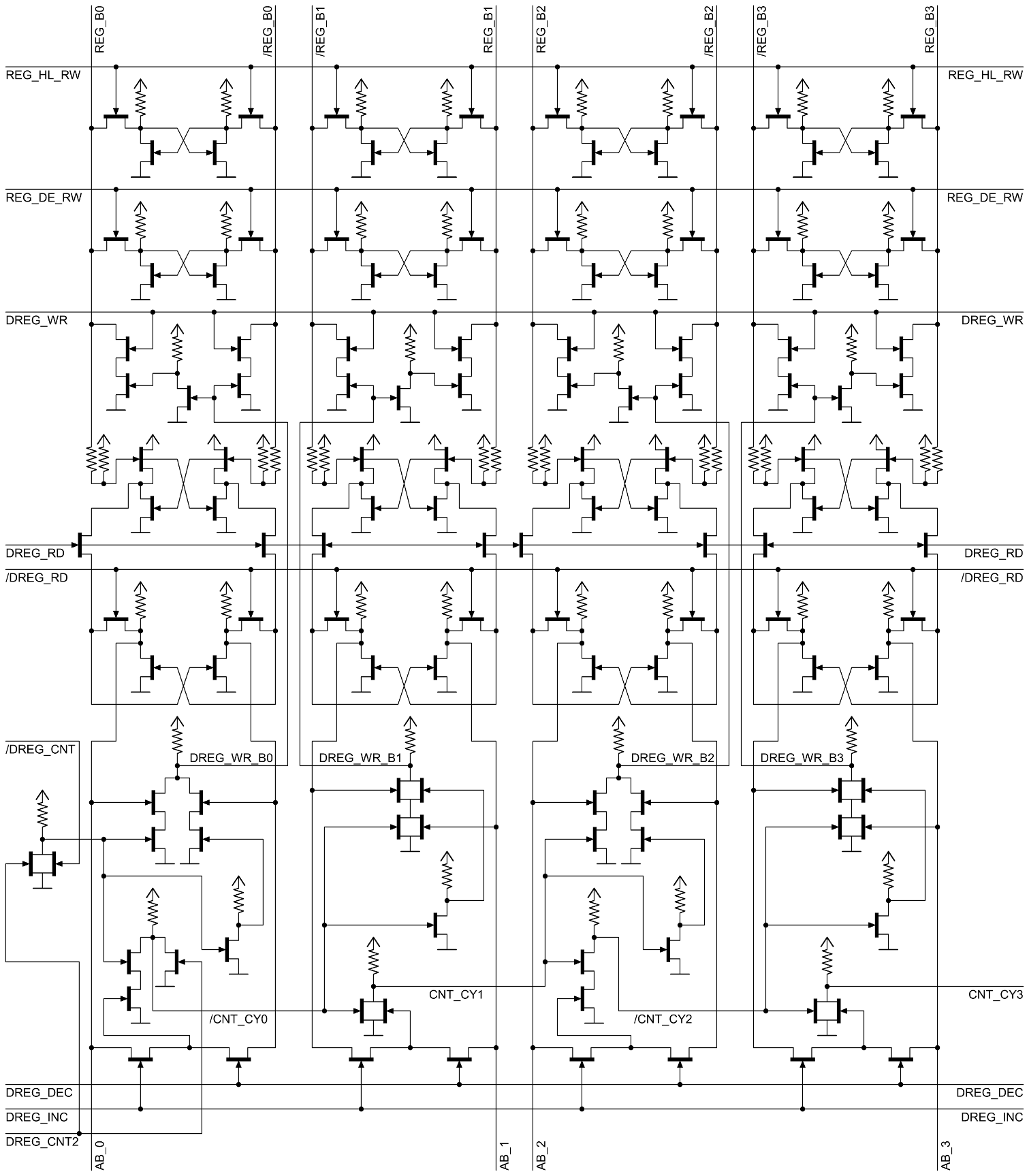
Overall architecture of the register file
The diagram below shows the implementation of the 8085 register file in the same layout as on the actual chip. The 8-bit data bus is at the top, and the 16-bit address bus is at the bottom. The register control lines are on the right.
In the middle are the registers, arranged as pairs of 8-bit registers.
Note that the registers are arranged "backwards" with the high-order bit on the right and the low-order bit on the left. The 16-bit program counter and stack pointer are first. Next is the WZ temporary register, and underneath it the BC register pair. The HL and DE register pairs are at the bottom - these registers do not have fixed locations, but can swap roles during execution. A 16-bit register bus (regbus) provides access to the registers.
Underneath the registers is the address latch, which holds a 16-bit value that is written to the address bus. This value is also the input to the 16-bit increment/decrement circuit. The output of the incrementer/decrementer can be written back to the registers.
The triangles indicate tri-state buffers, basically switches that control the flow of data. Buffers containing a + are amplifiers to boost the weak signals from the registers. Buffers containing a S are superbuffers, that provide extra current to send data across the long data bus.

Architecture diagram of the 8085 register file, as it is implemented on the chip. The register file is connected to the data bus at top, and address bus at bottom. The control lines are along the right.
The picture below zooms in on the chip image above, showing the register file in detail. The components in silicon exactly map onto the diagram above. Note the repeated patterns for the 16-bit circuits. The large transistors used as high-current drivers are clearly visible. The transistors in each bit of register storage are much smaller.

A closeup of the 8085 microprocessor, showing the details of the register file and the locations of the major components.
Storing bits in the register file
The implementation of the 8085 registers is unusual in several ways. The registers don't have explicit read and write modes; instead the register will be overwritten if there is a stronger signal on the bus. Instead of having a bus with one wire for each bit, the 8085 uses a sort of differential bus, with two wires for each bit: one wire transmits the value, and the other transmits the complement of the value.
Each bit consists of two inverters in a feedback loop, with pass transistors to connect the inverters to the bus. An unusual feature of this is the lack of any circuit to break the feedback loop when modifying the register (unlike the 6502). Instead, the 8085 uses a "might makes right" technique - if a stronger signal is written to the bus, it will overwrite a register connected to the bus.
The transistors driving the register bus are about twice as large as the transistors in the inverters, so they can forcibly overwrite the inverter loop.
One consequence of this register implementation is that a register can't be copied directly to another register, since there's nothing to distinguish the source register from the destination register - each register could potentially damage the other's bits. To get around this, the 8085 uses an interesting trick - copies are actually done through the ALU, as will be explained later.

One bit of a register in the 8085 register file. Each bit is stored in two inverters in a feedback loop. The register bus uses two lines of opposite polarity for each bit. Access to the register is controlled by the reg_rw control line, which connects the inverters to the bus, allowing the value to be read or written.
The image below zooms in on the chip closer, showing the silicon for six individual register bits. The schematic for one bit is overlaid, as are some of the metal lines providing power, ground, and the register bus. Each bit consists of two transistors for the inverters, two depletion pullup transistors for the inverters (shown as resistors), and two pass transistors connecting the bit to the register bus. The pink regions are transistors, with the green strips the gates (
details).

Detail of the 8085 chip showing six bits in the 8085's register file. Bit 2 of the stack pointer is shown with schematic. The two transistors form two inverters in a feedback loop. The light blue lines are the metal layer wires connected to bit 2. The program counter is in the upper half of the image.
To read a register, an amplifier circuit is used to boost the signal from the differential register bus to write it to the dbus or address latch. I assume this is a tradeoff to make the register file smaller. Each inverter pair can be made as small as possible, but then requires amplification to produce a signal strong enough for use elsewhere in the chip.
The amplification circuit that drives the data bus is more complex than I'd expect, probably because of the extra power to drive the bus (details and schematic).
The incrementer/decrementer
The 16-bit incrementer/decrementer at the bottom of the register file is used for multiple purposes. It increments the program counter as instructions execute, increments and decrements the stack pointer as needed, and supports the 16-bit increment and decrement instructions.
An interesting feature of the incrementer is it also supports incrementing by 2, which is used to quickly skip over the two byte address in a call or jump not taken. This allows these operations to complete faster on the 8085 than the 8080.

Two bits of the 16-bit increment/decrement circuit in the 8085. Odd bits and even bits use a different circuit for efficiency. The carry out from even bits is complemented.
The incrementer/decrementer is implemented by a chain of adders with ripple carry - the carry from each bit flows into the adder for the next bit. (The above schematic shows two bits, and is repeated 8 times in the full circuit.) The DREG_INC and DREG_DEC control lines select increment or decrement. One performance trick is that alternating bits are implemented with different circuits and the carry out of even bits is inverted. This avoids the inverters that would otherwise be needed to flip the carry back to its regular state. This saves space, but even more importantly it speeds up carry propagation. Because the carry has to propagate bit-by-bit through all 16 bits to generate the final result, adding an inverter to each bit would slow it down significantly.
The carry out is used to compute the undocumented K flag value (details).
In comparison, the 6502 has a 16-bit incrementer (no decrement) used exclusively by the program counter. To reduce the carry propagation speed, this incrementer uses a carry-skip. That is, the carry out of the low-order byte is immediately generated and fed into the high-order byte. Thus the carries only need to propagate through 8-bits, the two bytes working in parallel. (The carry is easily generated by ANDing together the low-order bits. If they are all 1, there will be a carry into the high-order byte.)
The WZ Temporary registers
The WZ register pair in the 8085 is used for temporary storage, but is invisible to the programmer. Internally, the WZ register pair is implemented like the other register pairs.
The primary use of WZ is to hold operands from a two or three byte instruction until it can be used.
The WZ registers are used to hold 16-bit addresses for LDA, STA, LHLD, JMP, CALL, and RST instructions. The registers hold the port for IN and OUT. The WZ register pair can also temporarily hold information read from memory. The registers hold the address popped off the stack for RET. For XTHL, the registers hold the value from the stack.
Register decoding and the instruction set
The instruction set of the 8085 is organized so an instruction can be quickly and easily decoded to determine the instruction to use.
The underlying structure for most 8085 instructions is the octal bit pattern bbDDDSSS, where destination bits DDD and/or source bits SSS select the register usage. The move (
MOV) instructions follow this structure.
Other instructions (e.g.
INR) use just the DDD bits to select the register, while math instructions use the three SSS bits.
Some instructions only use DDD or SSS, and some instructions operate on register pairs so they don't use the lowest bit. This instruction pattern is visible if the instructions are arranged in an
instruction table according to their octal values.
The three bits select the register as follows:
| D2D1D0 | Register |
|---|
| 000 | B |
| 001 | C |
| 010 | D |
| 011 | E |
| 100 | H |
| 101 | L |
| 110 | M |
| 111 | A |
M indicates a memory operation and is treated as a pseudo-register in the instruction set. Some instructions (e.g. INX) use the top two bits to select a register pair: BC, DE, HL, or "special" (stack pointer or accumulator).
Note that in the table above the low-order bit selects a register out of a register pair.
This instruction set structure allows simple logic to control the registers.
A multiplexer pulls out the right group of three bits, depending on the instruction and the cycle in the instruction
(link to schematic).
These three bits are then used to pick the specific register control lines to activate at each step.
The registers are controlled by about 18 control lines that affect the movement of data and the operation of the incremented/decrementer. The following table summarizes the control lines.
/RREG_RD | Reads the right-hand side register bus onto the data bus.
This implements the multiplexing of 16-bit registers onto the 8-bit data bus. |
/LREG_RD | Reads the left-hand side register bus onto the data bus. |
LREG_WR | Writes the data bus to the left-hand side register bus.
This implements the demultiplexing of the 8-bit data bus to the 16-bit registers. |
RREG_WR | Writes the data bus to the right-hand side register bus. |
REG_PC_RW | Connects the PC to the register bus. |
REG_SP_RW | Connects the SP to the register bus. |
REG_WZ_RW | Connects the WZ register pair to the register bus. |
REG_BC_RW | Connects the BC register pair to the register bus. |
REG_HL_RW | Connects the HL (DE) register pair to the register bus. |
REG_DE_RW | Connects the DE (HL) register pair to the register bus. |
DREG_WR | Writes the output of the incrementer/decrementer to the register bus. |
DREG_RD | Reads the register bus into the address latch. |
/DREG_RD | Inverted DREG_RD. |
DREG_DEC | Incrementer/decrementer performs decrement. |
DREG_INC | Incrementer/decrementer performs increment. |
CARRY_OUT | The carry/borrow out from the incrementer/decrementer. |
DREG_CNT | Increment/decrement by 1. |
DREG_CNT2 | Increment/decrement by 2. |
The first step in register control is the register control PLA, which generates 19 control signals based on the instruction type and the cycle step. The register control logic (between the register file and the PLA) mixes in the register selection bits as appropriate (and a few other inputs) to generate the register control lines listed above.
For instance, REG_BC_RW control line is activated if the PLA indicates a register access and the register bits are 00x. The RREG_RD control line is activated for a single-register read instruction if the register bits are xx0, and LREG_RD is activated if the bits are xx1. Both control lines are activated at the same time if the PLA indicates a register pair read.
The DE/HL exchange trick
The XCHG instruction exchanges the contents of the HL register pair with the contents of the DE register pair in a single M-cycle. You might wonder how the registers can be exchanged so quickly. It turns out that this instruction is implemented with a trick - an extra level of indirection.
Although most 8085 architecture diagrams label one register pair as DE and another as HL, this isn't exactly true.
In fact, the 8085 has two register pairs and either one can be the DE or HL pair. A status flip flop keeps track of which pair is DE and which is HL. As Pavel Zima figured out, the XCHG instruction doesn't move any data; it simply toggles the flip flop. The data remains in the same place, but the DE register is now HL and vice versa. Thus, the XCHG instruction is completed quickly. The consequence is every use of DE or HL uses this flip flop to determine which register to access
(link to schematic).
Using the ALU to move registers
You wouldn't expect the ALU (arithmetic-logic unit) to take part in a register-to-register move, but it happens in the 8085. Many register operations take advantage of the ALU's temporary registers.
The ALU doesn't directly operate on the accumulator and input register. Instead, the accumulator is copied to the ACT (Accumulator Temporary) register and the other input is copied to the TMP register. This way, the result can be written to the accumulator without the race condition that would occur if the accumulator were an input and output at the same time.
For register moves, the source value is copied to the TMP register, the ACT register is set to 0, and the ALU performs an OR operation
(ALU details), writing the result (i.e. the source value) to the dbus. This result can then be stored to the register file during a later cycle.
The register file in action
The step-by-step operation of the register file is surprisingly complex. One complication is that the register file and buses must handle stepping the program counter, fetching the instruction, and performing any register moves, without interference. A second complication is that register moves go through the ALU as described above.
Stepping through an operation in detail will show the complexity of the register operations. The following shows the data flow for a MOV B,E instruction, which copies the contents of the E register into the B register.
To understand this table, a bit of background on 8085 instruction timing. An instruction cycle is broken down into one or more M (machine) cycles, where an 8-bit memory access can be done in one M cycle. Each M cycle is broken down into several T-states, where each T-state corresponds to one clock cycle. Each clock cycle has a low phase and a high phase.
The single-byte register-to-register MOV instruction takes one M cycle (M1), 4 T cycles, or 8 clock phases. Each clock phase is a separate line in the table. To make things more complicated, the activity for an instruction isn't entirely within its own instruction cycle. To improve performance, the 8085 uses simple pipelining, where the M1 opcode fetch of the next instruction overlaps with completion of the previous instruction.
The MOV B, E instruction (which copies the E register to the B register) is illustrated in the table below. The PC is copied to the incrementer latch at the end of the previous operation, and then is written to the address pins during the T1 cycle. The PC is updated with the incremented value at the end of the T2 cycle.
The instruction opcode is fetched in the T3 cycle, and at this point execution can start on the instruction. It's not until the T1 cycle of the next instruction that the register file swings into action. The E register is written to the dbus at the end of the T1 cycle. Then the ALU's TMP register is loaded from the dbus. The ALU's other argument, the ACT register is 0 at this point, and the ALU is configured to perform an OR operation. At the end of the (next instruction's) T3 cycle, the result of the ALU operation (i.e. the E register) is stored in the B register via the dbus. Meanwhile, the next instruction is getting fetched (grayed out).
| Cycle | T/clock | PC action | Register action |
|---|
| T4/0 | | |
| T4/1 | PC → inc latch | |
M1
opcode fetch | T1/0 | inc latch → address pins | |
| T1/1 | inc latch → address pins | |
| T2/0 | | |
| T2/1 | inc → PC | |
| T3/0 | | data pins → dbus → instruction reg |
| T3/1 | | |
| T4/0 | | |
| T4/1 | PC → inc latch | |
M1
opcode fetch | T1/0 | inc latch → address pins | |
| T1/1 | inc latch → address pins | E reg → dbus |
| T2/0 | | dbus → TMP reg |
| T2/1 | inc → PC | |
| T3/0 | | data pins → dbus → instruction reg |
| T3/1 | | ALU → dbus → B reg |
Each step in the table above is activated by the appropriate register control lines. For instance, in T2/1, the PC is updated by triggering the reg_pc_rw and dreg_wr lines.
Conclusion
The 8085 has a complex register set, and it uses some interesting tricks to reduce the size of the chip and to optimize some operations. The register set is much harder to understand than I expected, but with careful examination it reveals its secrets.
Credits: The chip images are from visual6502.org. The visual6502 team did the hard work of dissolving chips in acid to remove the packaging and then taking many close-up photographs of the die inside. Pavel Zima converted these photographs into mask layer images, a transistor net, an 8085 simulator, and register file schematics (top, bottom).


