Reverse engineering the ARM1 processor's microinstructions

This article looks at how the ARM1 processor executes instructions. Unexpectedly, the ARM1 uses microcode, executing multiple microinstructions for each instruction. This microcode is stored in the instruction decode PLA, shown below. RISC processors generally don't use microcode, so I was surprised to find microcode at the heart of the ARM1. Unlike most microcoded processors, the microcode in the ARM1 is only a small part of the control circuitry.

Die photo of the ARM1 processor. Courtesy of Computer History Museum.

Die photo of the ARM1 processor. Courtesy of Computer History Museum.

I should warn the reader in advance that this article is more terse than my usual articles and intended for the small group of people interested in very low-level details of the ARM1. For the average reader I'd recommend my article Reverse engineering the ARM1 instead.

The microinstructions

Each instruction in the ARM1 is broken down into 1 to 4 microinstructions. These microinstructions are stored in the instruction decode PLA (which acts as a ROM).[1] The ARM1's microcode is stored as 42 rows of 36-bit microinstructions. The 42 rows are split into 18 classes of instructions, each consisting of 1 to 4 microinstructions. (The microcode sequencer supports looping, allowing it to handle the bulk data transfer instructions LDM and STM which can take up to 17 cycles.)

To explain the microinstruction format, I'll use the LDR instruction as an example. The LDR (Load Register) instruction accesses the memory address stored in a base register Rn plus a constant offset from the instruction and stores the result into a destination register Rd, also updating the base register. (This is similar to the C code: Rd = *Rn++;)[2] The ARM1 takes three cycles (i.e. three microinstructions) to perform this LDR operation. In the first cycle, the ALU adds the offset to the register to compute the address. The second cycle is used to fetch the word from memory. In the third cycle, the data is transferred to the destination register.

The diagram below shows the bit pattern for the LDR instruction. The PLA uses the highlighted bits (4, 20, 24-27) to determine the instruction class; the lighter bits are irrelevant for selecting the LDR instruction and are ignored. The cond bits specify a condition; if the condition is false, the instruction is skipped. The P, U, B, and W bits control different options for the LDR instruction. The Rn and Rd fields specify the base address register and the destination register. Finally, the 12-bit Offset field specifies the offset added to the base address.

Structure of the LDR (Load Register) instruction. Highlighted bits are used for instruction decoding; dark bits indicate LDR. Rn is the base register and Rd is the destination register.

Structure of the LDR (Load Register) instruction. Highlighted bits are used for instruction decoding; dark bits indicate LDR. Rn is the base register and Rd is the destination register.

Of the 32 instruction bits, only the 6 highlighted bits are used to select the microinstruction. As a result, microinstructions correspond to classes of instructions and the control outputs from the PLA are somewhat generic, e.g. "store to a register" rather than "store to register R12". Hardwired control logic looks at other bits in the instruction to pick a specific register, to pick a specific ALU operation, or to tweak exactly what the instruction does. For example, for LDR the microcode ignores the P, U, B and W bits and the hardwired control logic uses them. For registers, the microinstruction indicates which instruction bits specify the register and the hardwired register control logic uses those bits to select the register.

Contents of the microcode PLA

The raw data from the PLA for the LDR immediate instruction is given below, showing the 36 output bits forming a microinstruction for each cycle of the instruction.

Cycle numberPLA output
0001010101001000000100001100010100001
1101011010001000000001000111010100100
2010101101001000001010010110010010000

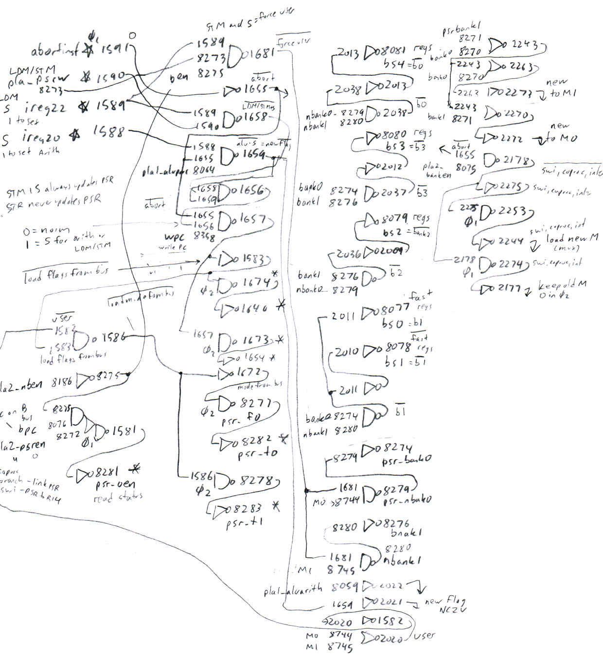
Since the raw PLA output is fairly meaningless, I have broken it down into fields and done a small amount of decoding. The image below shows the decoded contents of the instruction decode PLA; click for full-size. Each row corresponds to one clock cycle in an instruction and each column is one of the 22 fields generated by the 36 bits of the PLA. The PLA handles 18 different instruction groups, indicated on the left.

Contents of the ARM1 microcode PLA (thumbnail).

Contents of the ARM1 microcode PLA (thumbnail).

The rows Initialization and Interrupt are not instructions per se, but triggered by other PLA inputs. The Initialization micro-instruction is an idle step used when the pipeline does not have a valid instruction (at startup or after R15 modification). It is triggered if the iregval signal (8156) from the Pipeline State circuit is 0. The Interrupt microinstructions handle an interrupt or fault and are triggered by the intseq signal (8118) from the Trap Control circuit. The Reserved rows correspond to undocumented instructions, probably load and store with register-specified shift. The first Reserved row is unique in that the microcode sequence forks; this is cycle number 0 for both of the next Reserved blocks. It is unclear why these instructions were implemented but not documented.

Example microinstructions

The diagram below illustrates the three microinstructions that make up the load register immediate (LDR) instruction, with explanations on some of the important fields. The first microinstruction computes the address: the indicated fields instruct the ALU to add or subtract the 12-bit offset value from the instruction, and put the value on the address bus. The ALU control logic uses the U (up/down) and P (pre/posts) bits in the instruction to determine if the offset should be added or subtracted or ignored. This illustrates that the microinstruction only partially defines the instruction; the hardcoded control logic also makes decisions based on the instruction. The microinstruction also specifies that the sequencer should move to the next microinstruction.

The instruction decode PLA contents for the LDR (Load Register) immediate instruction. Each row corresponds to a clock cycles and shows the activity during one cycle. Each column indicates a control signal.

The instruction decode PLA contents for the LDR (Load Register) immediate instruction. Each row corresponds to a clock cycles and shows the activity during one cycle. Each column indicates a control signal.

The next microinstruction instructs the ALU to update the offset register. As before, the ALU control logic determines if the update requires an add or subtract. The register control logic determines if the register should be updated. The microinstruction also indicates that the fetched data should be read in.

The final microinstruction stores the fetched result in a register. It specifies Rd as the destination register and indicates a register write. The microinstruction tells the sequencer this is the end of the instruction.

Fields in the microinstruction

This section describes the fields that make up the microinstruction. I am still working out all the details, so this is not 100% accurate. Refer to the floorplan diagram below to see the components involved.

Floorplan of the ARM1 chip, from ARM Evaluation System manual. (Bus labels are corrected from original.)

Floorplan of the ARM1 chip, from ARM Evaluation System manual. (Bus labels are corrected from original.)

seqs: sequencer control

This field specifies the cycle number for the next microinstruction. It is used by the Sequence Controller. It has the following values:

FieldLabelMeaning
0ENDEnd of the instruction
1NEXTMove to next cycle in sequence
2IF23If not pencz, next cycle is 2; if pencz, next cycle is 3.
3IF1EIf not pencz, next cycle is 1; if pencz, ends the instruction.

The pencz signal from the priority encoder indicates all registers have been processed for a LDM/STM instruction.

For more information, see Reverse engineering ARM1 instruction sequencing.

Signal numbers: 8310, 8309. I've put this field first to make control flow clearer, but it is physically after rws in the PLA.

dinin: data in to B bus

This field indicates the value on the data pins should be read in to the B bus. It is used by the data bus controls.

Signal number: 8111

sctls: shifter controls

This field specifies the shifter action at a high level. The Shift Decode block uses this field in combination with other instruction bits and values to determine the specific shift direction and amount.

FieldShifter action
0Rs
1DP instruction
2ASL 2*instruction
3byte to word
4no shift
5ASL 2 bits
6nop (unused)
7nop

For more details, see Decoding barrel-shifter commands.

Signal numbers: 8288, 8287, 8286. Note that bits 2 and 1 are reversed coming out of the PLA.

aluac: ALU latch A bus

This signal latches the A bus value as an ALU input. The ALU control logic generates latch controls 2370, 2371 from this signal. For more details, see The ALU control logic.

Signal number: 8058

aluctls: ALU mode controls

This field selects the ALU mode. The ALU decoder uses this field to generate the ALU control signals.

FieldOperationInstructions
0add/rsb for base register update / addressLDM/STM/Data processing
1add for branch/fault destinationB/SWI
2add/sub/nop for address computationLDR/STR
3mov for register update, nop for abortLDM/LDR
4add/rsb/mov for address computationLDM/STM
5add/sub for base register updateLDR/STR
6rsb for link address updateBL / SWI
7op specified by instructionData processing

For more details, see The ALU control logic.

Signal numbers: 8062, 8061, 8060

aluenb: ALU latch B bus

This signal latches the B bus value as an ALU input. The ALU control logic generates latch controls 7485, 7486 from this signal. For more details, see The ALU control logic.

Signal number: 8063

banken: update PSR mode

This signal causes the M0, M1, F and I flags in the PSR to be updated from the psrbank signals from the trap control circuit. This happens during fault handling. This signal is used by the flag circuitry. For more details, see The ARM1 processor's flags.

Signal number: 8075

psrw: PSR write

This signal indicates that the PSR is potentially being written by a LDM/STM block copy instruction. It controls writing the ALU bus to the flags, after some more logic. It also allows LDM/STM to access the user-mode registers via the S bit. This signal is used by the flag circuitry. For more details, see The ARM1 processor's flags.

Signal number: 8273

nben: data to B bus

This signal indicates that the register file should write to the B bus when nben is 0. This signal is used by the register control logic and the flag logic. For more details, see The ARM1 processor's flags and Inside the ARMv1 Register Bank.

Signal number: 8186; the signal is negative-active.

psren: PSR to B bus

When active, this signal enables writing the PSR to the B bus to save it during a trap. This signal is used by the flag logic. For more details, see The ARM1 processor's flags.

Signal number: 8272

abctls: register controls for A and B bus

This field controls which registers are read onto the A and B bus. This signal is used by the register control logic.

FieldA register selectorB register selector
0Instruction bits 16-19 (Rn)Instruction bits 0-3 (Rm)
1Instruction bits 8-11 (Rs)Instruction bits 12-15 (Rd)
2R15Instruction bits 16-19 (Rn)
3R15From priority encoder
4Instruction bits 16-19 (Rn)R14

For more details, see Inside the ARMv1 Register Bank — register selection.

Signal numbers: 8042, 8041, 8040

wctls: register write controls

This field selects which register gets written to, from the ALU bus. This signal is used by the register control logic.

FieldRegister selector
0Instruction bits 16-19 (Rn)
1Instruction bits 12-15 (Rd)
2From priority encoder
3R14 (link)

For more details, see Inside the ARMv1 Register Bank — register selection.

Signal numbers: 8356, 8355

opc: OPC opcode fetch signal

This signal goes to the OPC pin and indicates a new instruction is being fetched. It is also used by the pipeline state circuitry.

Signal number: 8630

pipebl: pipeline control

This signal is used by the pipeline state circuitry. It apparently indicates the end of the instruction, except for STM. It is high throughout branches and faults, perhaps to clear the pipeline.

Signal number: 8261

skpwen: register write enable controls

This field controls whether a write to the register file happens or not. It is used by the Instruction Skip circuitry which can block the write if the instruction is aborted. The following table is a rough draft.

FieldWrite condition
0None
1Not dataabort
2Writeback
3Instruction bit 24 (link)
4Writeback / P bit
5alureg
6skpawen0

Signal numbers: 8324, 8323, 8322

skpw15: register 15 write controls

This signal controls writes to the R15 (PC). It is used by the Instruction Skip circuitry, perhaps to clear the pipeline when R15 is updated.

Signal number: 8321

skparegs: address bus controls

This field controls what is written to the address bus. It is used by the Instruction Skip circuitry to generate the address bus controls. The following table is a rough draft.

FieldAddress source
0Trap address
1ALU bus
2incrementer (normal) or ALU bus (for R15 write)
3unincremented PC (normal) or ALU bus (for R15 write)
4ALU bus or PC or incrementer, depending on R15 write and priority encoder
5ALU bus or PC or incrementer, depending on R15 write and priority encoder
6incrementer
7unincremented PC (normal) or ALU bus (for R15 write)

For more details, see Inside the ARMv1 — the Read Bus B, ALU Output Bus, and Address Bus.

Signal numbers: 8320, 8319, 8318

undef: undefined instruction

This signal is generated for an undefined instruction (specifically a coprocessor instruction). It is used by the Trap Control circuitry to generate a fault.

Signal number: 8348

rws: read or write select

This signal controls the RW output; it is 1 for a read and 0 for a write. The Trap Control circuitry gates this (apparently to block writes on an address exception) and the signal then drives the RW pin.

Signal number: 8284

pencen: priority encoder A bus control

This field controls writing of the bit counter output (times 4) to the A bus. It can also set the two low bits, either for the constant 3, or to add 3 to the bit counter output. The constant 3 is used (with borrow) to subtract 4 from R14 during a branch with link, see page 233 of VLSI RISC Architecture and Organization. The modified bit counter output is used to compute the LDM/STM start address.

FieldBit counter action on A bus
0None
1Low bits set (3)
2Bit count
3Bit count, low bits set

Signal numbers: 8202, 8201

bws: enable byte/word select

This signal indicates that byte/word should be selected by instruction bit 22, for LDR/STR. This signal is used by the Data Control (field extraction) circuitry.

For more details, see Inside the ARMv1 Read Bus.

Signal number: 8082

dctls: data bus field extraction controls

This field controls which bits of the data bus or instruction are passed to the B bus. This field is used by the Data Control (field extraction) circuitry.

FieldSelected data bus field
0Select a byte or word depending on bw
124 bits (branch offset)
212 bits (LDR/STR offset)
3byte (immediate instr)

For field 0, the byte is specified by controls 8195 and 8194.

For more details, see Inside the ARMv1 Read Bus or pages 296 and 301 of VLSI Risc Architecture and Organization.

Signal numbers: 8105, 8104

Microcode in RISC?

Everyone "knows" that RISC processors don't use microcode.[3] So does the ARM1 have "real microcode"?

One of the ARM1 architects explains microcode: "A microcode address is formed from some or all of the contents of the instruction register, together with some state values which are internal to the micro-control unit. This address is decoded to drive a unique row of a matrix, the columns of which are the control signals for the datapath."[4] This description is a perfect fit for how the ARM1's control works, so it seems reasonable to consider the ARM1 to have microcode.

I think it's easiest to understand the ARM1's control logic by viewing it as microcode. However, there are couple reasons to consider it not "real microcode". One reason is that the ARM1 microcode is only a small part of the chip's control, as you can see in the die photo and floorplan earlier. The control signals are heavily modified by the instruction skip component and conditionals are handled by the conditional unit. This goes beyond vertical microcode, where logic expands the microcode's control signals; in the ARM1, this other circuitry can entirely override the control signals. In addition, the ARM1 uses separate circuitry (the priority encoder) to control the block data transfer instructions; the microcode just sits in a loop. (The ARM2 is similar with multiplication — a separate circuit controls multiplication.)

The ARM1's microcode is an order of magnitude smaller than other microcoded processors. The ARM1's microcode has a 42×36 microcode, for 1512 bits in total. The 8086 used a 504×21 microcode (over 10,000 bits) while the 68000 has a 544×17 microcode and 366×68 nanocode (over 34,000 bits).

Probably the biggest objection to calling the ARM1 microcoded is that the designers of the ARM chip didn't consider it that way.[4] Furber mentions that some commercial RISC processors use microcode, but doesn't apply that term to the ARM1. He describes ARM1's instruction decode as two-level structure. In the first level, the instruction decoder PLA differentiates instructions into classes with similar characteristics. The secondary decoding uses the information from the first level along with hardware to cope with all the possible operations. The first level is described as providing "broad hints" about which functions to choose, and the second level fills in the details with bits from the instruction.

Conclusion

So is the ARM1 microcoded or not? The instruction decoder is clearly made up of microinstructions executed sequentially or with branching. It makes sense to look at this as microcode. But on the other hand, the microcode is fairly simple and forms a small part of the total control circuitry. A large amount of hardcoded logic interprets the microinstruction outputs to generate the control signals. My conclusion is the ARM1 should be called "partially microcoded" or maybe "hybrid microcode / hardwired control".

This article owes a lot to Dave Mugridge's analysis of the ARM1, especially Inside the ARMv1 — instruction decoding and sequencing. Thanks to the Visual 6502 team for the ARM1 simulator and data used in my analysis.

Notes and references

[1] While a typical PLA acts as structured logic gates generating signals (as in the Z-80 or 6502), the ARM1's PLA is different. Exactly one row is active at a time, so the PLA functions more like a ROM. There's a discussion of ROMs as PLAs in section 7.3.2.2 of The Architecture of Microprocessors.

[2] My explanation of the LDR instruction is simplified, since the instruction provides a variety of addressing mechanisms. It also provides byte access as well as 32-bit word access. Full details are here.

[3] IBM's ROMP microprocessor is generally considered RISC, but uses a 256×34 control ROM. Likewise, the Intel i960 is usually considered RISC but uses microcode.

[4] ARM1 designer Furber's book VLSI RISC Architecture and Organization discusses the ARM1 and other RISC chips. Section 1.3.1 has an extensive discussion of microcode. He describes how the ARM1's block move and ARM2's multiplication operations are under the control of a separate hardware unit inside the chip, unlike how a microcoded implementation would operate. Section 4.7 describes the ARM1's control logic.

555 timer teardown: inside the world's most popular IC

This article is translated into Vietnamese at: Bên trong chíp định thời 555.

If you've played around with electronic circuits, you probably know[1] the 555 timer integrated circuit, said to be the world's best-selling integrated circuit with billions sold. Designed by analog IC wizard Hans Camenzind[2] in 1970, the 555 has been called one of the greatest chips of all time with whole books devoted to 555 timer circuits.

Given the popularity of the 555 timer, I thought it would be interesting to find out what's inside the 555 timer and how it works. While the 555 timer is usually sold as a black plastic IC, it is also available in a metal can, which can be cut open with a hacksaw[3] revealing the tiny die inside.

Inside the 555 timer. The tiny die in the package is connected to the 8 pins by wires.

Inside the 555 timer. The tiny die in the package is connected to the 8 pins by wires.

A brief explanation of the 555 timer

The 555 timer has hundreds of applications, operating as anything from a timer or latch to a voltage-controlled oscillator or modulator. The diagram below illustrates how the 555 timer operates as a simple oscillator. Inside the 555 chip, three resistors form a divider generating references voltages of 1/3 and 2/3 of the supply voltage. The external capacitor will charge and discharge between these limits, producing an oscillation. In more detail, the capacitor will slowly charge (A) through the external resistors until its voltage hits the 2/3 reference. At that point (B), the upper (threshold) comparator switches the flip flop off and the output off. This turns on the discharge transistor, slowly discharging the capacitor (C). When the voltage on the capacitor hits the 1/3 reference (D), the lower (trigger) comparator turns on, setting the flip flop and the output, and the cycle repeats. The values of the resistors and capacitor control the timing, from microseconds to hours.[4]

Diagram showing how the 555 timer can operate as an oscillator.

Diagram showing how the 555 timer can operate as an oscillator.

To summarize, the key components of the 555 timer are the comparators to detect the upper and lower voltage limits, the three-resistor divider to set these limits, and the flip flop to keep track of whether the circuit is charging or discharging. The 555 timer has two other pins (reset and control voltage) that I haven't covered above; they can be used for more complex circuits.

The structure of the integrated circuit

The photo below shows the silicon die of the 555 through a microscope. On top of the silicon, a thin layer of metal connects different parts of the chip. This metal is clearly visible in the photo as yellowish-white traces and regions. Under the metal, a thin, glassy silicon dioxide layer provides insulation between the metal and the silicon, except where contact holes in the silicon dioxide allow the metal to connect to the silicon. At the edge of the chip, thin wires connect the metal pads to the chip's external pins.

Die photo of the 555 timer.

Die photo of the 555 timer.

The different types of silicon on the chip are harder to see. Regions of the chip are treated (doped) with impurities to change the electrical properties of the silicon. N-type silicon has an excess of electrons (negative), while P-type silicon lacks electrons (positive). In the photo, these regions show up as a slightly different color surrounded by a thin black border. These regions are the building blocks of the chip, forming transistors and resistors.

NPN transistors inside the IC

Transistors are the key components in a chip. The 555 timer uses NPN and PNP bipolar transistors. If you've studied electronics, you've probably seen a diagram of an NPN transistor like the one below, showing the collector (C), base (B), and emitter (E) of the transistor, The transistor is illustrated as a sandwich of P silicon in between two symmetric layers of N silicon; the N-P-N layers make an NPN transistor. It turns out that transistors on a chip look nothing like this, and the base often isn't even in the middle!

Schematic symbol for an NPN transistor, along with an oversimplified diagram of its internal structure.

Schematic symbol for an NPN transistor, along with an oversimplified diagram of its internal structure.

The photo below shows one of the transistors in the 555 as it appears on the chip. The slightly different tints in the silicon indicate regions that has been doped to form N and P regions. The whitish-yellow areas are the metal layer of the chip on top of the silicon - these form the wires connecting to the collector, emitter, and base. You can spot an emitter on the chip by its "bullseye" structure, while the base rectangle surrounds the emitter.

An NPN transistor in the 555 timer chip. The collector (C), emitter (E) and base (B) are labeled, along with N and P doped silicon.

An NPN transistor in the 555 timer chip. The collector (C), emitter (E) and base (B) are labeled, along with N and P doped silicon.

Underneath the photo is a cross-section drawing illustrating how the transistor is constructed. There's a lot more than just the N-P-N sandwich you see in books, but if you look carefully at the vertical cross section below the 'E', you can find the N-P-N that forms the transistor. The emitter (E) wire is connected to N+ silicon. Below that is a P layer connected to the base contact (B). And below that is an N+ layer connected (indirectly) to the collector (C).[5] The transistor is surrounded by a P+ ring that isolates it from neighboring components.

PNP transistors inside the IC

You might expect PNP transistors to be similar to NPN transistors, just swapping the roles of N and P silicon. But for a variety of reasons, PNP transistors have an entirely different construction. They consist of a small circular emitter (P), surrounded by a ring shaped base (N), which is surrounded by the collector (P). This forms a P-N-P sandwich horizontally (laterally), unlike the vertical structure of the NPN transistors.

The diagram below shows one of the PNP transistors in the 555, along with a cross-section showing the silicon structure. Note that although the metal contact for the base is on the edge of the transistor, it is electrically connected through the N and N+ regions to its active ring in between the collector and emitter. A metal line is routed between the collector and base, but is not part of the transistor.

A PNP transistor in the 555 timer chip. Connections for the collector (C), emitter (E) and base (B) are labeled, along with N and P doped silicon. The base forms a ring around the emitter, and the collector forms a ring around the base.

A PNP transistor in the 555 timer chip. Connections for the collector (C), emitter (E) and base (B) are labeled, along with N and P doped silicon. The base forms a ring around the emitter, and the collector forms a ring around the base.

The output transistors in the 555 are much larger than the other transistors and have a different structure in order to produce the high-current output. The photo below shows one of the output transistors. Note the multiple interlocking "fingers" of the emitter and base, surrounded by the large collector.

A large, high-current NPN output transistor in the 555 timer chip. The collector (C), base (B) and emitter (E) are labeled.

A large, high-current NPN output transistor in the 555 timer chip. The collector (C), base (B) and emitter (E) are labeled.

How resistors are implemented in silicon

Resistors are a key component of analog chips. Unfortunately, resistors in ICs are large and inaccurate; the resistances can vary by 50% from chip to chip. Thus, analog ICs are designed so only the ratio of resistors matters, not the absolute values, since the ratios remain nearly constant.

A resistor inside the 555 timer. The resistor is a strip of P silicon between two metal contacts.

A resistor inside the 555 timer. The resistor is a strip of P silicon between two metal contacts.

The photo above shows a 1KΩ resistor in the 555, formed from a strip of P silicon (visible as an outline). Note that the resistor connects two metal wires and another metal wire crosses it. The resistor below is an L-shaped 100KΩ pinch resistor. A layer of N silicon on top of the pinch resistor makes the conductive region much thinner (i.e. pinches it), forming a much higher but less accurate resistance.

A pinch resistor inside the 555 timer. The resistor is a strip of P silicon between two metal contacts. An N layer on top pinches the resistor and increases the resistance.

A pinch resistor inside the 555 timer. The resistor is a strip of P silicon between two metal contacts. An N layer on top pinches the resistor and increases the resistance.

IC component: The current mirror

There are some subcircuits that are very common in analog ICs, but may seem mysterious at first. The current mirror is one of these. If you've looked at analog IC block diagrams, you may have seen the symbols below, indicating a current source, and wondered what a current source is and why you'd use one. The idea is you start with one known current and then you can "clone" multiple copies of the current with a simple transistor circuit, the current mirror.

Schematic symbols for a current source.

Schematic symbols for a current source.

The following circuit shows how a current mirror is implemented with two identical transistors.[6] A reference current passes through the transistor on the left. (In this case, the current is set by the resistor.) Since both transistors have the same emitter voltage and base voltage, they source the same current, so the current on the right matches the reference current on the left.

Current mirror circuit. The current on the right copies the current on the left.

Current mirror circuit. The current on the right copies the current on the left.

A common use of a current mirror is to replace resistors. As explained earlier, resistors inside ICs are both inconveniently large and inaccurate. It saves space to use a current mirror instead of a resistor whenever possible. Also, the currents produced by a current mirror are nearly identical, unlike the currents produced by two resistors.

Three transistors form a current mirror in the 555 timer chip. They all share the same base and two transistors share emitters.

Three transistors form a current mirror in the 555 timer chip. They all share the same base and two transistors share emitters.
The three transistors above form a current mirror with two outputs. Note the three transistors share the base connection, tied to the collector on the right, and the emitters on the right are tied together. The transistor on the left is a Widlar current source, a modified mirror that produces a smaller current. On the schematic, the two transistors on the right are drawn as a single two-collector transistor, Q19.

IC component: The differential pair

The second important circuit to understand is the differential pair, the most common two-transistor subcircuit used in analog ICs.[7] You may have wondered how a comparator compares two voltages, or an op amp subtracts two voltages. This is the job of the differential pair.

Schematic of a simple differential pair circuit. The current sink sends a fixed current I through the differential pair. If the two inputs are equal, the current is split equally between the two branches. Otherwise, the branch with the higher input voltage gets most of the current.

Schematic of a simple differential pair circuit. The current sink sends a fixed current I through the differential pair. If the two inputs are equal, the current is split equally between the two branches. Otherwise, the branch with the higher input voltage gets most of the current.

The schematic above shows a simple differential pair. The current sink at the bottom provides a fixed current I, which is split between the two input transistors. If the input voltages are equal, the current will be split equally into the two branches (I1 and I2). If one of the input voltages is a bit higher than the other, the corresponding transistor will conduct more current, so one branch gets more current and the other branch gets less. A small input difference is enough to direct most of the current into the "winning" branch, flipping the comparator on or off.

In the 555, the threshold comparator uses NPN transistors, while the trigger comparator uses PNP transistors. This allows the threshold comparator to work near the supply voltage and the trigger comparator to work near ground. The 555's comparators also use two transistors on each input (Darlington pair) to buffer the inputs.

The 555 schematic interactive explorer

The 555 die photo and schematic[8] below are interactive. Click on a component in the die or schematic, and a brief explanation of the component will be displayed. (For a thorough discussion of how the 555 timer works, see 555 Principles of Operation.)

For a quick overview, the large output transistors and discharge transistor are the most obvious features on the die. The threshold comparator consists of Q1 through Q8. The trigger comparator consists of Q10 through Q13, along with current mirror Q9. Q16 and Q17 form the flip flop. The three 5KΩ resistors forming the voltage divider are in the middle of the chip.[9] Urban legend says that the 555 is named after these three 5K resistors, but according to its designer 555 is just an arbitrary number in the 500 chip series

Click the die or schematic for details...

How I photographed the 555 die

Integrated circuit usually come in a black epoxy package which require inconveniently dangerous concentrated acid to open. Instead, I bought a 555 in a metal can (below). To examine the die, I used a metallurgical microscope. Unlike a standard microscope, the metallurgical microscope shines light down through the lens allowing it to work with opaque objects (such as chips). I stitched the photos together with Hugin (details).

The 555 timer in a metal can package. (Banana for scale)

The 555 timer in an eight-pin metal can package. (Banana for scale)

The failed improved 555

Given the popularity of the 555, it's surprising that it has several rookie design flaws; unbalanced comparators, large operating currents, an asymmetric output waveform, and temperature sensitivity.[10]

In 1997, Camenzind redesigned the 555 to create a much better chip that could run at much lower voltages. The improved chip was sold by Zetex as the ZSCT1555, but unfortunately was a flop. The continuing success of the original 555 and the failure of the improved successor can be viewed as an example of the worse is better principle.

Conclusion

I hope you've found this look inside the 555 timer chip interesting. Next time you're building a 555 project, you'll know exactly what's inside the chip. If you enjoyed this article, I've also reverse-engineered the 741 op amp and 7805 voltage regulator. Thanks to Eric Schlaepfer[11] for helpful comments.

Follow me on Twitter and you won't miss an article!

Notes and references

[1] The 555 timer is iconic enough to appear on mugs, bags, caps and t-shirts.

The 555 timer is popular enough to appear on t-shirts. Courtesy of EEVblog.

The 555 timer is popular enough to appear on t-shirts. Courtesy of EEVblog.

[2] The book Designing Analog Chips written by the 555's inventor Hans Camenzind is really interesting, and I recommend it if you want to know how analog chips work. Chapter 11 has an extensive discussion of the 555's history and operation. Page 11-3 claims the 555 has been the best-selling IC every year, although I don't know if that is still true. The free PDF is here or get the book.

[3] You can cut an IC can open with a plain hacksaw, but a jeweler's saw gives a much cleaner cut. I got a jeweler's saw on eBay for $14, and used the #2 blade. Make sure you cut near the top of the IC so you don't hit the die as I did.

[4] The brilliant part of the 555 timer is that the oscillation frequency depends only on the external resistors and capacitor and is insensitive to the supply voltage. If the supply voltage drops, the 1/3 and 2/3 references drop too, so you might expect the oscillations to be faster. But the lower voltage charges the capacitor more slowly, canceling this out and keeping the frequency constant.

This voltage insensitivity is so tricky that the chip's designer didn't figure it out until near the end of the 555's design, but it made a big difference. The original design was more complex and required nine pins, which is a terrible size for an IC since there are no packages between 8 and 14 pins. The final, simpler 555 design worked with 8 pins, making the chip's packaging much cheaper. (See page 11-3 of Designing Analog Chips for the full story.)

[5] You might have wondered why there is a distinction between the collector and emitter of a transistor, when the typical diagram of a transistor is symmetrical. As you can see from the die photo, the collector and emitter are very different in a real transistor. In addition to the very large size difference, the silicon doping is different. The result is a transistor will have poor gain if the collector and emitter are swapped.

[6] For more information about current mirrors, check wikipedia, any analog IC book, or chapter 3 of Designing Analog Chips.

[7] Differential pairs are also called long-tailed pairs. According to Analysis and Design of Analog Integrated Circuits differential pairs are "perhaps the most widely used two-transistor subcircuits in monolithic analog circuits." (p214) For more information about differential pairs, see wikipedia, any analog IC book, or chapter 4 of Designing Analog Chips.

[8] The 555 schematic used in this article is from the Philips datasheet.

[9] Note that the three resistors for the voltage divider are parallel and next to each other. This helps ensure they have the same resistance even if there are electrical variations across the silicon.

[10] I'm not criticizing the 555; Hans Camenzind points out the design flaws and attributes them to "the early period of IC design (and the inexperience of a rookie designer)"; see Designing Analog Chips, page 11-4. The design of a 555 replacement is discussed in detail in "Redesigning the old 555", IEEE Spectrum, September 1997. That article makes it clear how much much faster IC design is now than in 1970. It took months to create the layout of the 555 chip by hand and manually verify it for correctness. The new chip took two days to layout and 20 minutes to verify.

[11] Evil Mad Scientist sells a very cool discrete 555 timer kit, duplicating the 555 circuit on a larger scale with individual transistors and resistors — it actually works as a 555 replacement. Their 555 footstool is also worth a look.

Large-size 555 timer created by Evil Mad Scientist Lab.

Large-size 555 timer created by Evil Mad Scientist Lab.

Reverse engineering ARM1 instruction sequencing, compared with the Z-80 and 6502

When a computer executes a machine language instruction, it breaks down the instruction into smaller steps that are performed in sequence. For instance, a load instruction might first compute a memory address, then fetch a value from that address, and then store that value in a register. This article describes how the ARM1 processor implements instruction sequencing, performing the right steps in order. I also look briefly at the 6502 and Z-80 microprocessors and the different sequencing techniques they use.

The die photo below shows the ARM1 processor chip, with the relevant functional blocks highlighted. This article focuses on the instruction sequence controller which moves step-by-step through an instruction in sequence. The instruction decode section specifies the steps that need to be performed for each operation and communicates with the sequence controller. The priority encoder tells the sequence controller when to stop block transfer instructions.

The ARM1 processor, showing the instruction sequencer and other parts of the chip that interact with the sequencer.

The ARM1 processor, showing the instruction sequence controller and other parts of the chip that interact with the sequence controller.

You might wonder what relevance a processor from 1985 has today. The ARM1 processor is the ancestor to the immensely popular ARM processor architecture that is used in smartphones and many other systems. Billions of ARM processors have been sold and you probably have one in your pocket now executing the same instructions I discuss in this article. I've written multiple articles about reverse engineering different components of the ARM1; start with my first article for an overview of the chip.

ARM1 instructions and their sequencing

Instructions on the ARM1 range from simple instructions that take one cycle to more complex multi-cycle instructions.[1] Some instructions, such as adding the values in two registers, don't require sequencing because they complete in a single clock cycle. The ARM1 instruction to load a register from memory (LDR) is more complex, consisting of three steps and requiring three clock cycles.[2] In the first step, the memory address is computed. In the second step, the data word is fetched from memory. At the same time, the address register is updated. In the final step, the data is stored into a register. The instruction sequence controller is responsible for stepping through these three steps.

The most complex instructions on the ARM1 are the block data transfer instructions, which read or write multiple registers to memory. A 16-bit bitmask in the instruction specifies the registers to transfer. The number of steps used by the instruction is variable because the read/write step is repeated up to 16 times to copy the specified registers, To support this, the sequence controller implements conditional loops. The ARM1 contains a priority encoder circuit that scans through the register selection bits in order and signals the sequence controller when the transfers are done.

The sequence controller

The instruction sequence controller on the ARM1 is responsible for sequencing the steps of an instruction by providing a cycle number (0 to 3). It also must restart at the end of each instruction. It must repeat cycles as necessary for block transfers.[3]

To move between steps, the sequence controller has four sequence operations that it can perform each clock:

END: the instruction ends and an new instruction starts next step.
NEXT: the sequence controller moves to the next cycle number.
IF23: this conditional provides branching and looping for block data transfer —if not done, it stays on cycle 2; otherwise it goes to cycle 3.
IF1E: similar to IF23, if not done, it stays on cycle 1; otherwise it goes to the end cycle (0).

How does the sequence controller know which operation to perform? This information, along with the other control signals, is provided by the instruction decoder. The instruction decoder can be thought of as holding 42 microinstructions, each 36 bits wide.[4] The instruction decoder provides the appropriate microinstruction for each instruction type and cycle number. These microinstruction bits generate control signals for the chip.[5] Two bits in the microinstruction (seqs1 and seqs0) provide the operation to the sequence controller, indicating how to compute the next cycle number. Normally this will be NEXT, until the last microinstruction which specifies END. Thus, the instruction decoder and the sequence controller work together: the sequence controller's cycle number tells the instruction decoder which microinstruction to use, and the instruction decoder tells the sequence controller how to compute the next cycle number.

The sequence controller circuit

Schematic of the instruction sequencing circuit from the ARM1 processor.

Schematic of the instruction sequencing circuit from the ARM1 processor.

The schematic above shows the circuitry for the instruction sequence controller. The overall idea is the instruction decoder indicates how to compute the next cycle through signals seqs1 and seqs0. The sequence controller produces outputs seq1 and seq0, which tell the instruction decoder the next cycle number. The next cycle values are selected by two multiplexers, which pick one of the four input values based on the control inputs, as shown in the following table. The loop values depend on the pencz signal from the priority encoder, which indicates no more registers to process.

InputSeq1Seq0
00 (END)00
01 (NEXT)seq1' xor seq0'not seq0'
10 (IF23)1pencz
11 (IF1E)0not pencz

It's straightforward to verify that this logic implements the sequencing described earlier:

Input 00 (END) results in output cycle 0.
Input 01 (NEXT) increments the old cycle (seq1', seq0') by 1.
Input 10 (IF23) will output cycle 2 until pencz is triggered, and then output cycle 3.
Input 11 (IF1E) will output cycle 1 until pencz is triggered and then output cycle 0, the END cycle.

The schematic shows that the sequence controller circuit provides two other outputs. In cycle 0, the circuit outputs the newinst signal, indicating to the rest of the chip that a new instruction is starting. The abortinst signal indicates that the instruction should not be executed because its condition was not satisfied. It is based on the skip input, which comes from the conditional instruction circuit, and is set if the instruction should be skipped.[6] If the instruction should be skipped, abortinst is asserted in cycle 0, forcing the next cycle to be 0 and terminating the instruction after a single cycle. The abortinst signal is also used elsewhere to prevent the skipped instruction from having any effect. Thus, a skipped instruction is effectively a one-cycle NOP instruction.

The implementation of this circuit uses a two-phase clock and dynamic latches to move from step to step. The multi-triangle symbol in the schematic is a transmission gate, used frequently in the ARM1 to build dynamic latches. A transmission gate can be thought of as a switch that closes during the specified clock phase. When the switch opens, the charge stored on the capacitance of the wire holds the previous value, forming a dynamic latch. The clock itself is two phase: First the Φ1 signal is high and the Φ2 is low, and then they alternate. One transmission gate is open during Φ1 and the other is open during Φ2. You can think of it like people moving through double doors: when the first door is open, they can move through it, but must wait for the second door to open. In this manner, the signal progresses through the circuit under the control of the clock and the cycle count updates once per complete clock cycle.

Comparison with the 6502's control logic

This section briefly looks at the 6502 chip, which uses different techniques for sequencing instructions. The 6502 controls each instruction by stepping sequentially through a time step each clock cycle: T0 through T6. Some instructions are quick, ending after two cycles, while others can take all 7 cycles. Instead of a binary counter, the 6502 keeps track of the current T cycle with a shift register with a single active bit that indicates the current cycle (a ring counter). That is, a separate control line is activated during each T cycle, which makes the rest of the control logic easier to implement. When the last T cycle for a particular instruction is reached, the control logic generates a signal (inexplicably called METAL) to reset the shift register to T0 for the next instruction.[7]

Interesting 6502 fact: if you execute an illegal instruction known as KIL (kill), the T reset signal doesn't get generated and the timing bit falls off the end of the shift register. The 6502 ends up in no T state at all and stops generating control signals. This locks up the chip until a hardware reset is triggered.

Layout of the 6502 processor.

Layout of the 6502 processor. Die photo courtesy of Visual 6502.

The die photo above shows the layout of the 6502 processor. Note that the control logic (Decode PLA and Random control logic[8] ) takes up about half the chip. At the top, the PLA (Programmable Logic Array) implements the first step of decoding. Below that, the gate logic generates the control signals, using the PLA outputs. The datapath in the bottom part of the chip contains the registers, ALU (arithmetic logic unit), and buses. It performs the operations as instructed by the control signals.

The PLA is a structured collection of NOR gates, which is visible in the die photo as a regular grid. It takes as inputs the instruction and the timing state, and outputs 130 different control signals, which indicate a combination of a timing state and instruction class, such as "T1.DEX" or "T4.X,IND". The PLA outputs are combined and processed by many gates to generate the final control signals, for instance S/SB (connecting the S and SB buses) or SUM (instructing the ALU to compute a sum).

To compare the ARM1 and 6502, they both use sequential timing states to control the instructions but the implementations are different. The 6502 uses a shift register to sequentially move through states. The more complex sequence controller in the ARM1 provides looping on a state. The 6502 has more states (7 vs 4), but looping in the ARM1 allows longer instructions. The ARM1's sequence controller is highly structured, with sequencer "commands" generated by the PLA; an END command reset the sequence controller to end each instruction. The 6502 uses a combination of a PLA and hard-wired logic to control the sequence; the METAL signal resets the shift register to end each instruction.

Comparison with the Z-80's control logic

The Z-80 uses a much more complicated system for instruction sequencing. An instruction is made up of multiple M (memory) cycles, one for each memory access during the instruction. Each M cycle consists of multiple T (time) states. For example an instruction could take 3 T states for the first M cycle and 4 for the second, going through the states: M1T1, M1T2, M1T3, M2T1, M2T2, M2T3, M2T4. More complex instructions can have 6 machine cycles and 23 T states.

Layout of the Z-80 processor.

Layout of the Z-80 processor. Data courtesy of Visual 6502.

The diagram above shows the layout of the Z-80. The control logic consists of the circuitry to generate the state timing signals, the PLA that decodes instructions,[9] and the random logic to generate control signals below. The chip's datapath (registers and ALU) are at the bottom of the chip. (You may be surprised that the Z-80 has a 4-bit ALU.)

The Z-80's control logic is implemented using a shift register ring counter for the M cycles and a second shift register ring counter for the T states. At the end of an M cycle, the M cycle counter advances to the next cycle and the T state counter resets. Like the 6502, the Z-80 uses a PLA and random logic for instruction decoding, but the details are different. The Z-80 has an AND/OR PLA that generates outputs for different instruction classes, from a single instruction like "LD SP, HL" to larger classes such as a conditional jump or a load. In comparison, the 6502's PLA has a single NOR plane that combines both instruction decoding and timing.

The Z-80 uses complex gates to combine the instruction signals with the timing signals to generate the control signal. A typical gate is structured as: "generate a signal to do something for instruction X in M1T1 or instruction Y in M2T3 or instruction Z in M2T6". The chip layout for these signals has an interesting structure, shown below: the signals T1 to T5 and M1 to M5 run horizontally in the metal layer (faint gray), while the instruction signals (A, B, C) run vertically in polysilicon wires (green). Transistors (yellow) are formed where polysilicon wires cross the silicon (red). This creates a complex, multi-input AND/NOR gate that generates a control signal for the right combination of M, T, and instruction signals. Due to the structure of MOS circuits, this complex gate is constructed as a single gate.

One gate from the Z-80 to generate a control signal at the right time by combining M cycle and T state signals.

One gate from the Z-80 to generate a control signal at the right time by combining M cycle and T state signals. Neighboring gates have similar structures to generate other control signals.

The AND/NOR gate above computes not ((A and M4 and T3) or (B and M3 and T5) or (C and M1 and T2)). It has three vertical red paths from ground to the output (one uses a hard-to-see horizontal metal connection); since any of these paths can form a connection this creates a three-input NOR gate. Each path has three yellow transistors; all three transistors must be active to complete the path, so this forms a three-input AND gate.

In this gate, A, B, and C are instruction decode signals. Signal A, for instance, is triggered by an indexed load instruction. The output of this gate controls writes to the registers. Thus, an indexed load instruction will trigger the control signal at time M4 T3, causing a register write. To summarize, the Z-80 uses gates such as these to generate control signals when instructions are at a specific point in the M and T cycle.

The Z-80's instruction sequencing is much more complex than the ARM1 and 6502. The Z-80 sequences instructions through M cycles, each of which is composed of multiple T states. Like the 6502, the Z-80 uses a combination of a PLA and random logic to generate the control signals. The 6502 combines instruction decoding and timing signals in the PLA, while the Z-80 uses the PLA only for instruction decoding. The Z-80 uses complex multi-input gates to generate control signals by combining the decoded instructions with timing signals. Like the ARM1, the Z-80 can loop over states to support block data operations.

Conclusion

The ARM1, Z-80 and 6502 use very different techniques for sequencing instructions. The ARM1 can use a simple, highly structured sequence controller because of its simple RISC instruction set. The 6502 and Z-80 are implemented with a PLA in combination with hard-wired "random" logic. You can see these chips in action with the Visual 6502 team's simulators: Visual ARM1 simulator and Visual 6502 simulator.

For more articles on ARM1 internals, see my full set of ARM posts and Dave Mugridge's series of posts. This article builds on Dave's article on Instruction decoding and sequencing. Thanks to the Visual 6502 team for providing the die photos and chip layout used in this analysis.

Follow me on Twitter here for updates on my latest articles.

Notes and references

[1] The ARM1 is a reduced instruction set computer (RISC) with relatively simple instructions. The typical RISC chip performs at most one memory access per instruction, making instruction sequencing straightforward. However, the ARM1 processor has instructions that are more complex than typical for a RISC processor, such as block data transfer instructions that can access 16 memory words. Some people suggest the ARM is not really RISC, but the R in ARM does stand for RISC.

[2] The LDR (Load Register) instruction described is is similar to the C statement Rd = *Rn++;, but it can do more. I've simplified the explanation of the LDR instruction since it provides a variety of addressing mechanisms. Full details are here.

[3] The ARM1 uses state looping for the block data transfer instructions. The ARM2 also uses the same loop functionality for multiplication and coprocessor operations. (Multiplication uses Booth's multiplication algorithm, invented in 1950. The multiplier does shifts and adds until all the bits are handled.) The book VLSI Risc Architecture and Organization by ARM architect Furber briefly discusses the sequence controller on page 303.

[4] See the article Inside the ARMv1 —instruction decoding and sequencing for discussion of how instruction decoding works in the ARM1. The instruction decoder is implemented with a PLA (Programmable Logic Array). It may be controversial to call its rows microinstructions, but I think that's the best way to understand its operation. Unlike the PLA in the 6502 or Z-80, the ARM1's instruction decode PLA operates more like a ROM, with exactly one row active at a time, and it steps through these rows sequentially. These rows can be considered microinstructions that generate the control signals. I wouldn't call the ARM1 more than partially microcoded because the majority of the chip's control logic is hardwired.

[5] For an example of microinstructions, consider the load register instruction described earlier that takes three cycles. It has three microinstructions. The control signals specified by the first microinstruction tell the ALU to add the base register and offset, put this on the address bus, and perform a memory read. The second microinstruction tells the ALU to compute the new base register value and write it to the register. The third microinstruction stores the fetched value in the destination register and terminates the instruction. Thus, each cycle of an instruction has a microinstruction specifying what to do during that cycle.

[6] An instruction is skipped if the condition is false, the instruction is not an undefined instruction, and a fault is not in progress. As a consequence, an undefined instruction will cause an exception even if its condition is false and it wouldn't be executed.

[7] The first two timing states in the 6502 (T0 and T1) are more complex than a shift register in order to handle some special cases and to optimize two-cycle instructions.) For more information on 6502 instruction sequencing, see 6502 State Machine and How MOS 6502 Illegal Opcodes really work. The contents of the 6502 PLA are described here.

[8] "Random logic" describes unstructured logic that appears random; it isn't actually random, of course.

[9] The regular grid structure of the AND plane of the Z-80's decode PLA's is visible in the layout diagram. The structure of the OR plane is less visible, since the PLA has been optimized so multiple terms can fit in one row. For more than you ever wanted to know about PLA optimization in early microprocessors, see The Architecture of Microprocessors by F. Anceau, 1986. This book is a wealth of information on microprocessors of the early 1980s, but is dense and somewhat academic.

The ARM1 processor's flags, reverse engineered

This article reverse-engineers the flag circuits in the ARM1 processor, explaining in detail how the flags are generate, controlled, and used. Condition flags are a key part of most computers, since they allow the computer to change what it does based on various conditions. The flags keep track of conditions such as a value being negative or zero or an overflow happening. Processors may also have status flags to control modes such as running in user mode versus protected (kernel) execution. The ARM1 processor stores these flags in a special register called the Processor Status Register (PSR).[1]

The ARM1 chip is interesting to examine not only because it is simple enough to understand but also because it was the first ARM processor. There are now tens of billions of ARM processors in use, probably powering your smartphone right now. This article is part of my series on reverse-engineering the ARM1. Processor flags seem like they should be trivial, but there's a lot more involved than you might expect. You might want to start with my first article for an overview of the chip.

The die photo below shows the ARM1 chip. This article concentrates on the flag logic, highlighted in red. As you can see, flags take up a significant part of the chip. The flags interact with many other parts of the chip: the trap control logic handles interrupts and exceptions; the register control logic handles access to the chip's registers including the program counter (PC); when the Arithmetic-Logic Unit (ALU) performs computations it stores status in the flags; the Barrel Shifter shifts or rotates values, sending shifted bits to the flags; and the Instruction Register holds instructions as they are read from memory and feeds them to the decode logic to be interpreted. In the upper left, the M0 and M1 pins indicate the mode bits stored in the flags. The article will describe how all these components interact with the flags.

The flag circuitry in the ARM1 processor interacts with many other components of the chip.

The flag circuitry (red) in the ARM1 processor interacts with many other components of the chip. Original photo courtesy of Computer History Museum.

Some ARM1 background

This section summarizes a few features of the ARM1 processor that are important for understanding the flags. The ARM1 is a 32-bit processor with 16 32-bit registers called R0 through R15 (and some extra registers that will be described later). The processor has a 26-bit address space.

One unusual feature of the ARM1 processor is it combines the flag bits in the processor status register (PSR) and the program counter (PC) into a single register, R15, the PC/PSR. Because of the 26-bit address space, the top 6 bits of the 32-bit PC register are unused. In addition, instructions are always aligned on a 32-bit boundary, so the bottom two PC bits are always 0. These eight unused PC bits were instead used for flags, as shown in the diagram below.[2]

The Processor Status Register in the ARM1 processor is combined with the program counter.

The Processor Status Register in the ARM1 processor is combined with the program counter. From page 2-26 of the ARM databook.

Four condition flags hold the status of arithmetic operations or comparisons. The negative (N) flag indicates a negative result. The zero (Z) flag indicates a zero result. The carry (C) flag indicates a carry from an unsigned value that doesn't fit in 32 bits. The overflow (V) flag indicates an overflow from a signed value that doesn't fit in 32 bits. The next two bits are used to enable or disable interrupts: the I flag controls regular interrupts, while the F flag controls the chip's special fast interrupts. The bottom two bits (M1 and M0) control the processor's execution mode: user, supervisor (kernel), interrupt handler, or fast interrupt handler. These modes will be discussed in more detail later.

Two instruction classes that are important to flags are the data processing instructions and the block data transfer instructions. Since the ARM has a simple, orthogonal instruction set, these operations can operate on the R15 with the flags as easily as any of the other registers.

The data processing instructions are the arithmetic-logic instructions. There are 16 types of data processing operations, such as addition, subtraction, Boolean operations such as AND, and comparison. Unlike most processors, the ARM makes updates of the condition flags optional. The instruction includes a bit called the "S" bit. If the S bit is set, the instruction updates the condition flags; otherwise the flags remain unchanged. The data processing instructions can also act on R15 directly, causing the flags to be read or modified.

The ARM also provides block data transfer instructions: LDM (load multiple) and STM (store multiple). These instructions load a selected set of registers from memory or store them to memory, for example popping registers from the stack or pushing them to the stack. These instructions can also use R15, accessing or modifying the flags.

Floorplan of the ARM1 chip, from ARM Evaluation System manual. (Bus labels are corrected from original.)

Floorplan of the ARM1 chip, from ARM Evaluation System manual. (Bus labels are corrected from original.)

While the program counter (PC) and flags are architecturally part of the same register R15, they are physically separated on the chip, as you can see from the die photo and the floorplan diagram above. The flags are labeled PSR, above the ALU, while the PC is on the left of the register file. Interestingly, the original sketch for the ARM1 (below) show the PSR flags right next to the PC. While the final chip architecture largely matched the sketch, some components moved. In particular, several functional units were moved to the top of the chip, above the instruction bus (orange).

Original sketch of the ARM1 chip layout. Note the Processor Status Register (PSR) is on the left; the final chip put it above the ALU. Photo courtesy of Ed Spittles.

Original sketch of the ARM1 chip layout. Note the Processor Status Register (PSR) is on the left; the final chip put it above the ALU. Photo courtesy of Ed Spittles.

The flag circuitry

The diagram below shows the flag circuit of the chip as it appears in the simulator; this is a zoomed-in version of the red rectangle indicated on the die earlier.

The chip consists of multiple layers, indicated by different colors below. Transistors appear as red or blue regions. NMOS transistors are red; they turn on with a 1 input and can pull their output low. PMOS transistors (blue) are complementary; they turn on with a 0 input and can pull their output high. Physically above the transistors is the polysilicon wiring layer (green). When polysilicon crosses a transistor it forms the gate (yellow) that controls the transistor. Finally, two layers of metal wiring (gray) are above the polysilicon.

The flag circuit in the ARM1 processor. The eight flags are at the bottom, with control circuitry above.

The flag circuit in the ARM1 processor. The eight flags are at the bottom, with control circuitry above.

The flag circuit above has been partitioned into several components. At the bottom are the circuits to store the eight flags. In the upper left, the flag control circuitry generates signals that control flag use and updates. The mode control circuit in the upper right generates the signals to update the mode bits M0 and M1. Finally, the register control circuit uses the mode bits to select a register bank. At the bottom is the wiring that connects the B bus, ALU bus, and flag inputs to the flag circuits.

The remainder of this article will start by discussing a single flag, the N flag at the bottom. Next it will describe the condition flags (V, C, Z and N) in more detail, along with how the flag control circuit (schematic) creates the control signals. This will be followed by an explanation of the mode flags (M0, M1) and the interrupt flags (F, I) and their control signals. The article ends with a discussion of the register bank select circuit.

The circuit to store a flag

This section discusses how the negative (N) flag works. The other flags operate similarly, but with some differences, and will be discussed in later section. The schematic below shows the circuit for the negative flag; this flag is at the bottom of the chip layout above. If you're expecting flags to be stored in a flip flop or regular latch, this circuit may seem unusual. Flags are stored in a dynamic two-phase flip-flop, which uses stray capacitance to store the value. The basic idea is the value goes around in a loop, amplified by the four inverters, and controlled by the clock. The trapezoids in the schematic are pass-transistor multiplexers[3] Each multiplexer has two inputs and two control lines; if a control line is active, the corresponding input is connected to the output.

Circuit for one flag (N) in the ARM1. The flag is stored in a two-phase dynamic latch. Two multiplexers (trapezoids) select values to store in the flag.

Circuit for one flag (N) in the ARM1. The flag is stored in a two-phase dynamic latch. Two multiplexers (trapezoids) select values to store in the flag.

The storage loop consists of two parts, alternately connected by the clock. During the first clock phase, Φ1, the multiplexer on the left is inactivated by its inputs and generates no output. It holds its previous output due to stray capacitance at the point marked "hold during Φ1". The signal goes around the loop, through the Φ1 transistor on the right, and up to the input of the multiplexer. When the clock switches to Φ2, the multiplexer becomes active again, and the transistor on the right switches off. Now, the signal to the left of the transistor is held by the capacitance and flows around the loop until it reaches the transistor and is blocked. Thus, during each clock phase, half the loop is stable and half the loop can be updated. Alternatively, you can consider each half a simple latch and the two parts form a master-slave latch.

The main use of the condition flags is for conditional instructions — executing an instruction if the condition is satisfied. The flag out wire in the diagram goes to the conditional instruction logic which controls execution by checking the flag values to determine if the condition is satisfied (details),

The typical way the condition flags are updated is after performing a data processing operation, e.g. ADD. If the result is negative, the N flag is set; otherwise, the N flag is cleared. The multiplexer on the right allows the new flag value from the ALU to be selected instead of the recirculating value. This happens if the aluflag control signal is activated.

The second way to update the condition flags is to write to them directly, for instance to restore the flag values after handling an interrupt. The flags can be written from the ALU data bus (which is different from the flag value from the ALU described earlier). The multiplexer on the left selects this value instead of the recirculating value if the writeflags signal is active.

The condition flags can be read directly, for instance to save the flag values while handling an interrupt. The transistors on the left allow the flags to be written to the B bus when the psr_oen (PSR output enable) control signal is activated.

The diagram below zooms in on the chip layout of the N flag, which can be compared with the schematic. The wire that recirculates the flag from the right to the left is indicated. You can see the transistors that form the inverters and multiplexers. Details on how the red NMOS transistors and blue PMOS transistors work together to form inverters are here.

The circuitry for one flag (N/negative) in the ARM1 processor.

The circuitry for one flag (N/negative) in the ARM1 processor.

The conditions flags in detail

The flags all roughly follow the circuit described above, but there are differences since the flags have different behaviors. The schematic below shows the circuits for the four condition flags: V, C, Z and N. This section describes these flags in detail, along with how the control signals are generated. By comparing the chip logic with the documentation, we can see how the described behavior is implemented in the logic.

Generating the flags

Each flag is generated in a different way. The N (negative) flag is very simple. A signed number is negative if the top bit is set, so the N flag is simply loaded from the top bit of the ALU bus.

The Z (zero) flag is generated by the ALU. The ALU in effect does a NOR of all 32 output bits; if all bits are zero, the Z flag is 1. For efficiency, the ALU uses a chain of alternating NAND and NOR gates, but the effect is the same.

Generating the C (carry) flag is quite complicated. For arithmetic operations, the carry flag is the carry out from bit 31 of the ALU: this is the carry for addition and not-borrow for subtraction. The ARM1 supports a variety of shift operations, which affect the carry in different ways, so logic gates select different bits from the shifter depending on the instruction. It may be the bit shifted out on the left, the bit shifted out on the right, the carry flag, the left bit or the right bit.

The V (overflow) flag indicates overflow of a signed value. If two signed values are added or subtracted, the result may not fit in 32 bits, and this is indicated by setting the overflow flag. An overflow occurs if the carry out from bit 30 being different from the carry out from bit 31 and is computed by XOR of these two bits. I discuss signed overflow in detail here.

Schematic of the condition flags in the ARM1 processor: oVerflow, Carry, Zero, and Negative.

Schematic of the condition flags in the ARM1 processor: OVerflow, Carry, Zero, and Negative.

Updating the condition flags with results of an operation

One feature that distinguishes the ARM processor from most other processors is that condition flag updates are optional. If an arithmetic operation has the S bit (bit 20) set, the flags are updated, otherwise they are not. By looking at how the aluflag control signal is generated, we can see how this functionality is implemented.

The ARM manual explains how flags are updated by a data processing instruction (ADD, etc.)

The ARM manual explains how flags are updated by a data processing instruction (ADD, etc.)

If the aluflag control signal[4] is high, the multiplexer on the right will select the flag value generated by the ALU, rather than the recirculated value. The aluflag control signal is activated if pla1_aluproc from the instruction decoder is set (details) and if the S bit (bit 20) is set in the instruction register. The pla1_aluproc line is set when the ALU is doing a data processing operation, but not when the ALU is, for example, computing an address offset. This is why the condition flags are updated only for relevant operations. If an abort of the instruction occurs, aluflag is blocked, preventing the flags from being modified.

Arithmetic versus logic operations

The following text from the ARM databook explains the behavior of the condition flags during a data processing (ALU) operation. The part of interest is that the carry (C) and overflow (V) flags are treated differently for logical operations versus arithmetic operations.

The ARM manual explains how arithmetic and logic operations update the flags differently.

The ARM manual explains how arithmetic and logic operations update the flags differently.

The schematic shows the circuits that explain this behavior. The control line pla1_aluarith is generated by the instruction decode logic (details); it is high if the ALU operation is an arithmetic operation (e.g. ADD), and low for a logic operation (e.g. AND). This control line selects the different C and V inputs for arithmetic or logical operations. For the C flag, this control line selects between the ALU's carry out and the shifter's carry out. (The shifter has a lot of logic because the carry out depends on the type and direction of shifting.) For the V flag, this control line selects between the ALU's overflow signal and the old V flag — this is why logic operations don't update the V flag.

Writing the flags directly

As described earlier, the flags and the Program Counter share register R15, so storing a value in R15 can update the flags. This is implemented through the multiplexer on the left. If control signal writeflags is activated, the multiplexer on the left will select the value from the ALU bus, rather than the recirculated value, updating the flags with the new value. Otherwise, nowriteflags is activated, selecting the recirculated value and leaving the flag unchanged. (Note that both writeflags and nowriteflags are inactive during clock phase Φ1, effectively disconnecting the multiplexer output.)

The generation of writeflags is relatively complicated. First, if pla_psrw this indicates a block copy instruction (LDM/STM) is writing to the PSR; if instruction register bit 22 (S) is set the flags will be updated. Second, aluflag (described above) indicates an ALU data processing operation should update the flags. In either of these cases, as long as abort is clear, and wpc (write PC) is set, then the nowriteflags1 signal is active. This signal is combined with the clock Φ2 to generate the writeflags and opposite nowriteflags signals sent to the multiplexer. This implements the logic described on page 2-34 for data processing instructions:

The ARM manual explains how flags are updated by the LDM block transfer instruction.

The ARM manual explains how flags are updated by the LDM block transfer instruction.

Reading the flags

Looking at the block diagram of the ARM1 process explains some of the behavior when reading the flags. A data processing instruction specifies three registers: the operation is performed on the first two registers and the result stored in the third. The first register (Rn) is read over the A bus. The second register (Rm) is read over the B bus and goes through the barrel shifter. The ALU generates the result of the operation, which is stored to a third register (Rd) via the ALU bus.

Block diagram of the ARM1 processor showing the flags.

Block diagram of the ARM1 processor showing the flags. The flags are read via the B bus and written via the ALU bus. The flags also receive values directly from the ALU and shifter.

The block diagram above shows how the flags are connected to the chip's buses. The flags are separate from the register file; they are written via the ALU bus and read via the B bus. Thus, the flag value in R15 can only be accessed as the second register (Rm) via the B bus, and not as the first register (Rn) via the A bus. This explains the behavior described in the manual:

Depending on how it is accessed, register R15 in the ARM1 may or may not provide the flag values. From the manual.

Depending on how it is accessed, register R15 in the ARM1 may or may not provide the flag values. From the ARM databook, page 2-35.

The process to write data to the B bus may seem backwards. The B bus is complemented, so a 1 on the bus indicates a 0 value. In more detail, the B bus is pulled high in clock phase Φ2 by transistors on the right of the register file (details). In clock phase Φ1, anyone writing to the bus sends a 1 by pulling the corresponding bus line low.[5] From the schematic, you can see that the control signal psr_oen (PSR output enable) controls putting the (complemented) flag values on the B bus. If psr_oen is active (only in phase Φ1) and the flag value is 1, the output transistors will pull the bus to 0.

The psr_oen signal is enabled to read the flags in two cases. The first happens when flags are being saved to R14 for a trap. The pla2_psren (PSR enable) signal controls this; it comes from instruction decoding at the start of a software interrupt (SWI), coprocessor instruction (i.e undefined instruction), or interrupt. The second case is when the R15 is being read via the B bus. This is indicated when pla2_ben (B Enable) and bpc (B bus PC) are active. The pla2_ben signal (PSR enable) comes from instruction decoding and is enabled at some point during most instructions. The register file generates the bpc signal when the B bus accesses the PC.

The mode and interrupt flags

This section discusses the M0 and M1 (processor mode) flags and the I and F (interrupt) flags. The behavior of these flags is different in several ways from the condition code flags, and their circuitry is significantly different.

The four modes of the ARM1 are:

M1M0Mode
00User
01Fast Interrupt (FIRQ)
10Interrupt (IRQ)
11Supervisor (SVC)

When an exception trap occurs, the trap logic directs the flag circuitry to switch the mode. An interrupt switches to Interrupt mode, a fast interrupt switches to Fast Interrupt mode, and any other exception (reset, undefined instruction, memory abort, etc) switches to Supervisor mode. The trap logic indicates the new mode through the signals psrbank1 and psrbank0:

Exceptionpsrbank1psrbank0
Fast Interrupt01
Interrupt10
Reset11
Other00

Note that the psrbank values don't exactly match the M0/M1 values. The psrbank values pass through a few gates in the mode control logic to generate newM1 and newM0 which are stored into the flags.

As the schematic shows, control signal oldstatus causes the flags to keep their old value, while newstatus loads the new value when a fault occurs. The newstatus signal is generated from instruction decode signal pla2_banken, which is activated during a SWI (software interrupt) instruction, coprocessor instruction (causing an undefined instruction fault), or an interrupt. It is blocked by the abort signal. Otherwise oldstatus is activated. Both signals can only be active during clock phase Φ1.

Schematic of the status flags in the ARM1 processor: Mode 0 and 1, Interrupt, and Fast interrupt.

Schematic of the status flags in the ARM1 processor: Mode 0 and 1, Interrupt, and Fast interrupt.

The other multiplexer signals are psr_t0, which loads the flags from the ALU bus, and psr_t1, which uses the value from the previous multiplexer. Both signals can be active only during clock phase Φ2, so the two multiplexers alternate. The psr_t0 signal is the same as writeflags used by the condition flags, except it is blocked if the mode flags indicate user mode. This is how the ARM1 prevents the mode and status flags from being updated in User mode (which is necessary for security). The psr_t1 signal is the opposite of psr_t0 (not exactly inverted since both are low during Φ1).

Moving on to the interrupt flags, any fault causes the I flag to be set (preventing an interrupt while the fault is being handled). This is accomplished by the 1 input to the I register multiplexer. The F flag is set (blocking fast interrupts) on reset and when a fast interrupt occurs. The schematic shows that F will be set if psrbank0 is high, and keeps its old value otherwise (via the OR gate). Since psrbank0 is high for fast interrupts and reset, the desired behavior is obtained.

One interesting thing about the M0 and M1 flags is they are connected directly to the M0 and M1 output pin driver circuits, shown below. This circuit supports tri-state output (electrically disconnecting the output so the signal can be controlled externally) as well as input, even though neither of these features is used for the M0 and M1 pins. The reason is the same pin driver circuit is reused for all the ARM1 output pins regardless of whether or not they need these features. This is another example of how the ARM1 was designed for simplicity, rather than optimizing the design. Note that large transistors to provide the output current to the pin.

Driver for the M0 mode output pin. Much of the circuit is unused, since the same circuit is used for most I/O pins.

Driver for the M0 mode output pin. Much of the circuit is unused, since the same circuit is used for most I/O pins.

Register control

One feature of the ARM1 processor is has multiple register banks, controlled by the mode flags. While there are 16 logical registers (R0 through R15), there are 25 physical registers. Each of the four modes has its own R13 and R14. The fast interrupt mode also has its own R10, R11 and R12.[6] These register banks improve performance by allowing interrupt handlers to use registers without needing to save the user registers.

The flag circuitry generates the signals that select the register bank. These signals go to the registers control circuitry next to the registers, where they are used to select particular registers details). The bank select signals are
bs0: general (non-fast-interrupt) registers.
bs1: fast interrupt registers.
bs2: regular interrupt registers.
bs3: supervisor registers.
bs4: user registers.

These (low-active) signals are generated from the M0 and M1 flags, which specify the mode. Registers R10-R12 use bs0 and bs1 to select the appropriate bank for fast interrupts or otherwise. Registers R13 and R14 use bs1, bs2, bs3 and bs4 to select between the four register banks.

One complication is for LDM/STM instruction, the S flag causes the user register bank to be used instead of the expected register bank. (This is a feature so interrupt handlers can access user registers if desired.) This happens if the pla2_psrw line is high, indicating a LDM/STM instruction; instruction register bit 22 is high (the S bit for LDM/STM); and pla2_nben is low, indicating bus B enabled. The pla2_psrw and pla2_nben signals are generated by the instruction decode circuits (details).

Conclusion

I expected to write a brief article on the ARM1 flags, but the topic turned out to be more complex than I expected. This article got a bit out of hand, so congratulations if you made it to the end! The flags are not the simple 8-bit register I expected, but are stored in dynamic latches with many control lines and inputs. With careful examination, it is possible to explain how the features and special cases described in the manual are implemented in the circuits. Studying the flags also explains the function of several of the control signals generated by the instruction decoder.

Now that you've seen the internals of the flag logic, you can use the Visual ARM1 simulator to see the circuit in action. Thanks to the Visual 6502 team for providing the simulator and ARM1 chip layout data. For more articles on ARM1 internals, see my full set of ARM posts and Dave Mugridge's series of posts.

For my latest articles, follow me on Twitter here.

Notes and references

[1] Flags do not need to be bits in a register. The IBM 1401 and Intel 8008, for instance, do not have status flags as part of a register. Flags in these computers were not assigned bit positions but exist more abstractly. The Z-80 on the other hand, stores flags both in discrete latches and in a flag register, copying the flags between the two. The MIPS architecture doesn't have condition flags at all, but does both the test and the branch in the conditional branch instructions.

[2] Was combining the flags and program counter into a single register in the ARM1 a clever idea or just bizarre? On the positive side, this allowed the flags and PC to be saved or restored in a single transfer, rather than two operations. It also allowed flags to be accessed without special flag instructions. On the negative side, restricting the address space to 26 bits was bad in the long term. This decision also prevented adding more flags in the future. Combining the flags and PC in register R15 also required special-case handling for R15 for many instructions.

The ARM architecture moved away from the combined PC/flags with the ARMv3 architecture. The flags were moved to separate registers: CPSR (Current processor status register) and SPSR (Saved Processor Status Register), allowing 32-bit addressing as well as additional flags and modes. New instructions (MSR, MRS) were added to access the CPSR and SPSR. (One ARMv3 processor of note is the ARM610, used in the Apple Newton.) Details on the historical and modern ARM status registers are here.

(The ARM numbering scheme is rather confusing. Architecture version numbers (e.g. ARMv3) don't match up with the CPU numbers (e.g. ARM6). More information on the ARM family numbering is here.)

[3] I discussed how the multiplexers in the ARM1 work earlier. In brief, each input has an NMOS and PMOS transistor working together as a switch, allowing the input to be connected to the output. The schematics show a single control line for each input; the implementation has two lines since the PMOS control signal must be inverted.

[4] Each signal in the simulator has a reference number that can be used to cross-reference the signals in other articles. Here are the key control signals used in the flags circuitry and their reference numbers:

abort1591, 1655
aluflag2021
bpc8076
bs08077
bs18078
bs28079
bs38080
bs48081
instruction reg 228141
instruction reg 208139
newM02273
newM12272
newstatus2244
nowriteflags1654
nowriteflags11657
oldstatus2177
pla_psrw8273
pla1_aluarith8059
pla1_aluproc8064
pla2_banken8075
pla2_ben8275
pla2_nben8186
pla2_psren8272
pla2_psrw8273
psr_oen8281
psr_t08282
psr_t18283
psrbank08270
psrbank18271
wpc8358
writeflags1640

[5] You might wonder why the bus works in this way. This clocked dynamic logic is simpler than using logic gates to control the signal on the bus; only two transistors are needed to write a bit to the bus and they can be attached to the bus at any location. But why complement the bus? The reason is that it's easier with CMOS to pull a line low than to pull a line high. An NMOS transistor can provide more current than a similar PMOS transistor. And the reason for that is electrons (which carry the charge in NMOS) move faster than holes (which carry the charge in PMOS). Ultimately, the B bus is complemented due to semiconductor physics. (The Z-80 is another chip that has as complemented data bus.)

[6] Later versions of the ARM architecture introduced additional modes and more duplicated banks. Details are at ARMwiki.