Die analysis of the 8087 math coprocessor's fast bit shifter

Floating-point numbers are very useful for scientific programming, but early microprocessors only supported integers directly.1 Although floating-point was common in mainframes back in the 1950s and 1960s, it wasn't until 1980 that Intel introduced the 8087 floating-point coprocessor for microcomputers.2 Adding this chip to a microcomputer such as the IBM PC made floating-point operations up to 100 times faster. This was a huge benefit for applications such as AutoCAD, spreadsheets, or flight simulators.3 The downside was the 8087 chip cost hundreds of dollars.4

It's hard to implement floating-point operations so they are computed quickly and accurately. Problems can arise from overflow, rounding, transcendental operations, and numerous edge cases. Prior to the 8087, each manufacturer had their own incompatible ad hoc implementation of floating point. Intel, however, enlisted numerical analysis expert William Kahan to design accurate floating point based on rigorous principles.5 The result was the floating-point architecture of the 8087. This became the IEEE 754 standard used in almost all modern computers, so I consider the 8087 one of the most influential chips ever designed.

Die of the Intel 8087 floating point unit chip, with main functional blocks labeled. The die is 5mm×6mm. The shifter is outlined in red. Click for a larger image.

Die of the Intel 8087 floating point unit chip, with main functional blocks labeled. The die is 5mm×6mm. The shifter is outlined in red. Click for a larger image.

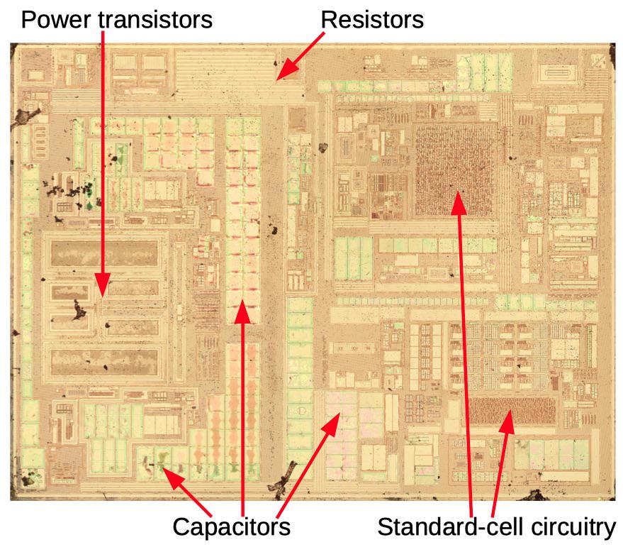
To explore how the 8087 works, I opened up an 8087 chip and took photos of the silicon die with a microscope. Containing 40,000 transistors, the 8087 pushed chip manufacturing to the limit; in comparison, the companion 8086 microprocessor only had 29,000 transistors. To make the chip possible, Intel developed new techniques. In this article, I focus on the high-speed binary shifter (outlined in red above). The shifter takes up a large fraction of the chip's area, so minimizing its area was vital to making the 8087 possible.

A floating-point number consists of a fraction (also called significand or mantissa), an exponent, and a sign bit. (These are expressed in binary, but for a base-10 analogy, the number 6.02×10²³ has 6.02 as the fraction and 23 as the exponent.) The circuitry to process the fraction is at the bottom of the die photo. From left to right, the fraction circuitry consists of a constant ROM, a shifter (highlighted), adder/subtracters, and the register stack. The exponent processing circuitry is in the middle of the chip. Above it, the microcode engine and ROM control the chip.

The shifter

The role of the shifter is to shift binary numbers left or right, a task with several critical roles in floating-point operations. When two floating-point numbers are added or subtracted, the numbers must be shifted so the binary points line up. (The binary point is like the decimal point, but for a binary number.) The 8087's transcendental instructions are built around shift and add operations, using an algorithm called CORDIC. The shifter is also used to assemble a floating-point number from 16-bit chunks read from memory.8

Since shifts are so essential to performance, the 8087 uses a "barrel shifter", which can shift a number by any number of bits in a single step.6 Intel used a two-stage shifter design that kept its size manageable while still providing high performance. The first stage shifts the value by 0 to 7 bits, while the second stage shifts by 0 to 7 bytes. In combination, the two stages shift a value by any amount from 0 to 63 bits.

The bit shifter

I'll start by describing the bit shifter, which performs a shift of 0 to 7 bit positions. The diagram below outlines the structure of the bit shifter, showing five of the inputs and outputs; the full shifter supports 68 bits.7 The concept is that by activating a particular column, the input is shifted by the desired amount. Each circle indicates a transistor that can act as a switch between an input line and an output line. The vertical select lines are used to activate the desired transistors. Each input line is connected diagonally to eight transistors, allowing it to be directed to one of eight outputs. For example, the diagram shows shift select line 3 activated, turning on the associated transistors (green). The highlighted input 20 (orange) is directed to output 23 (blue). Similarly, the other inputs are connected to the corresponding outputs, yielding a shift by 3. By activating a different shift select line, the input will be shifted by a different amount between 0 and 7 bits.

Structure of the bit shifter. By energizing a shift select line, the inputs are connected to outputs with the desired bit shift.

Structure of the bit shifter. By energizing a shift select line, the inputs are connected to outputs with the desired bit shift.

To explain the internal construction of the shifter, I'll start by describing the NMOS transistors used in the 8087 chip. Transistors are built by doping areas of the silicon substrate with impurities to create "diffusion" regions with different electrical properties. The transistor can be considered a switch, controlling the flow of current between two regions called the source and drain. The transistor is activated by the gate, made of a special type of silicon called polysilicon, layered above the substrate silicon. Applying voltage to the gate lets current flow between the source and drain, which is otherwise blocked. Transistors are wired together by a metal layer on top, building a complex integrated circuit.

Structure of a MOSFET as implemented in an integrated circuit.

Structure of a MOSFET as implemented in an integrated circuit.

The photo below shows a transistor in the 8087 as it appears under the microscope. Its structure matches the diagram above, although its shape is more complex. The source, gate, and drain all continue out of the photo, connected to other transistors. In addition, wiring in the metal layer is connected to the silicon at the circular vias. (The metal layer was removed with acid for this photo.)

An NMOS transistor in the 8087 chip, as seen under the microscope.

An NMOS transistor in the 8087 chip, as seen under the microscope.

Zooming out, the diagram below shows part of the bit shifter as implemented on the chip. About 48 transistors, similar to the one above, are in this photo. The orange and yellow diagonal corresponds to one of the inputs: the orange regions show transistors connected through the silicon, while the yellow lines show connections in the metal layer. (The metal layer is used to jump over the polysilicon select lines.) The green highlight shows the polysilicon line for shift-by-three. In the center, this polysilicon gate line turns on a transistor, connecting the input to the long yellow output line, shifting the highlighted input by three positions. (The other non-highlighted inputs are shifted similarly.) Thus, this circuit implements the shifter as described at the beginning of the section. The photo shows six of the 68 inputs, so the complete shifter is much taller.

Closeup of the silicon circuitry for the bit shifter. The path of one signal is shown, as controlled by the shift-by-three control (green).

Closeup of the silicon circuitry for the bit shifter. The path of one signal is shown, as controlled by the shift-by-three control (green).

The byte shifter

The byte shifter shifts its inputs by multiples of eight bits, rather than one bit. Its design is similar to the bit shifter, except each input connects to every eighth output. For instance, input 20 connects to outputs 20, 28, 36, and so forth, shifting by bytes. As a result, the diagonal connections are steep and packed tightly, with eight lines between each switch. In the diagram below, the line for shift-by-four is selected, with the connection from input 0 to output 32 highlighted. Note the lack of wires in the right half of the diagram because any bit shifted from beyond input 0 becomes zeroed. For instance, when shifting left by 4 bytes, low-order bits 31 and below become zero.

The structure of the byte shifter.

The structure of the byte shifter.

The die photo below shows part of the bit shifter and the byte shifter. This photo is zoomed-out to show the overall structure; individual transistors are barely visible. The bit shifter's area is densely packed with transistors, but the byte shifter consists mostly of wiring, with columns of transistors in between.9 Also note that the byte shifter is partially empty at the top, filling in with more wiring towards the bottom. The wiring layout isn't as orderly as in the diagram above, but is arranged for maximum efficiency.

The bit shifter and byte shifter in the 8087 chip.

The bit shifter and byte shifter in the 8087 chip.

The bidirectional drivers

So far, the bit and byte shifters only shift bits in one direction.11 However, bits need to be shifted in both directions. One of the key innovations of the 8087's shifter is its bidirectional design: data can be passed through the shifter in reverse to shift bits the opposite direction. This is possible because the shifter is constructed with pass transistors, not logic gates. Pass transistor logic uses transistors as switches that pass or block signals, so signals can travel in either direction. (In contrast, regular logic gates such as NOR gates have specific inputs and outputs.)

Special driver circuitry on the left and right sides of the shifter allows the shifter to operate in either direction. To send data from left to right, the left-hand driver reads data from the fraction bus and sends it into the shifter. The right-hand driver circuit receives this shifted data, latches it temporarily, and then writes it back to the fraction bus. To send data in the opposite direction, the driver circuits reverse roles: the right-hand driver sends data from the fraction bus into the shifter while the left-hand circuit receives the shifted data.10

The multiplexer / decoders

The final feature I'll describe is the circuitry that controlled the shifter. Three different sources control how many positions to shift. First, the microcode engine can specify the number directly. Second, the number can come from a loop counter; this is used as part of the CORDIC transcendental algorithms. Finally, the number can come from a leading zero counter; this allows numbers to be normalized by eliminating leading zeroes through shifting. Each of these sources provides a 6-bit shift number; the six multiplexers each select one bit from the desired source.12

The multiplexer/decoder circuitry.

The multiplexer/decoder circuitry.

Next, decoders activate one of eight bit-shift lines and one of eight byte-shift lines to control the appropriate pass transistors in the shifter. (Each decoder takes a 3-bit input and activates one of 8 output lines.) Because each decoder line controls a large column of pass transistors in the shifter, the decoder uses relatively large power transistors.13 At the bottom, the 16 control lines exit the circuitry.

Conclusion

The 8087 is a complex chip with many functional units. However, by examining the die closely, the circuits of the 8087 can be understood. This blog post described the 8087's fast barrel shifter, capable of shifting by up to 63 bits at a time.14 Intel received a patent on this innovative programmable bidirectional shifter.

The shifter was just one of the features that let the 8087 compute floating-point operations much faster than the 8086 processor could. The 8087 operates on 80 bits at a time instead of 16. The 8087 has 80-bit wide registers, reducing memory accesses during computations. The 8087 stores constants for transcendental operations in a ROM, also avoiding memory accesses. Hardware in the 8087 checked for NaN, underflow, overflow, etc., avoiding slow checks in code. The 8087's hardware made multiplication and division faster. I don't know the relative contributions of these factors, but in combination, they improved floating-point performance dramatically, by up to a factor of 100.

The benefits of floating point hardware are so great that Intel started integrating the floating-point unit into the processor with the 80486 (1989). Now, most processors include a floating-point unit and the expense of purchasing a separate floating-point coprocessor is a thing of the past.

Die photo of the 8087 with the metal layer removed. The colors are due to some of the oxide layer remaining. Click for a larger image.

Die photo of the 8087 with the metal layer removed. The colors are due to some of the oxide layer remaining. Click for a larger image.

For more information on the 8087, see my other articles: Extracting ROM constants from the 8087, The two-bit-per-transistor ROM and The substrate bias generator. I announce my latest blog posts on Twitter, so follow me @kenshirriff for future articles. I also have an RSS feed.

Notes and references

  1. Even without floating-point hardware, early microcomputers could perform floating-point operations. The operations would be broken down into many integer operations, manipulating the exponent and fraction as necessary. In other words, floating-point support didn't make floating-point operations possible, it just made them much faster. (Another way to represent non-integers is fixed-point numbers, which have a fixed number of digits after the decimal. Fixed-point numbers are simpler than floating-point, but can't represent as large a range.) 

  2. The 8087 wasn't the first floating-point chip. National Semiconductor introduced the MM57109 Number Cruncher Unit (that is the real name) in 1977. It was essentially a repackaged 12-digit scientific calculator chip, operating on binary-coded decimal values with values entered in Reverse Polish Notation. This chip was absurdly slow; a tangent, for instance, could take over a second. AMD introduced their floating-point chip, the Am9511, in 1978 (details). This chip supported 32-bit floating-point numbers and took up to 1.4 milliseconds for a tangent. (Intel ended up licensing the Am9511 from AMD and selling it as the 8231.) A 10-MHz 8087 in comparison, could do a tangent in 54 microseconds, operating on an 80-bit floating-point number. Thus, the 8087's performance and accuracy were far superior to previous chips. 

  3. The original IBM PC (1981) had an empty socket on its motherboard for adding an 8087 coprocessor. a huge benefit for applications such as AutoCAD. The large empty socket is visible in the upper left below, above the 8088 microprocessor. A list of applications with support for the 8087 is here.

    Motherboard of the original IBM PC (1981).
Photo from Wikimedia, CC BY-SA 3.0.

    Motherboard of the original IBM PC (1981). Photo from Wikimedia, CC BY-SA 3.0.


  4. I couldn't find the original price for the 8087, but it was expensive. At first, Intel only sold the 8087 as a matched and tested pair with an 8088, due to timing flakiness with the 8087. By 1982, Intel dropped the price of the 8087 to $230, equivalent to about $500 in current dollars. Compared to today's open-source world, it seems strange that customers also had to pay for software support: using the 8087 with the BASIC language cost another $150, while Intel's 8087 development library was $1250. 

  5. The designers of the 8087 commented on the guidance offered by Professor Kahan: "We did not do as well as he wanted, but we did better than he expected." Kahan later received a Turing Award for his work on floating point.  

  6. Processors often include a variety of shift instructions, including rotate operations that shift bits from one end of the word to the other. The 8087 only performs straight shifts, not rotates. 

  7. The shifter handles the 8087's 64-bit fraction, along with three extra bits for rounding accuracy, so it supports 67 bits. Unless I miscounted, the shifter also has an extra bit in the most significant position, making it 68 bits wide. 

  8. Multiplication and division make heavy use of shifting; multiplication is performed by shifts and adds, while division uses shifts and subtracts. However, the 8087 does not use the general-purpose shifter for these operations, but has specialized shifters optimized for these operations. 

  9. In order to pack the wiring as close together as possible, the shifter alternated wires of diffused silicon and wires of polysilicon. In the photo below, the diffused silicon wires are pinkish, while the polysilicon is yellowish. The 8087 was built with Intel's HMOS III process, which required a 4µm spacing for polysilicon and 5µm for diffusion, probably due to the resolution of the photolithography practice. However, the spacing between a diffusion line and a polysilicon line could be much smaller, probably because they were created with separate masks and were on separate layers. Thus, alternating diffusion and polysilicon lines could be packed together tightly, saving space.

    Wiring in the byte shifter consists of alternating, tightly-packed silicon and polysilicon lines. The large rectangles on either side are pairs of transistors, controlled by vertical polysilicon lines.

    Wiring in the byte shifter consists of alternating, tightly-packed silicon and polysilicon lines. The large rectangles on either side are pairs of transistors, controlled by vertical polysilicon lines.

  10. The driver circuitry has a few subtleties. Instead of sending data directly into the shifter, bits are transferred in two steps. First, the shifter lines are pre-charged to a high level. Then, any 1-bit inputs cause the corresponding shifter lines to be pulled low. In other words, the shifter lines are active-low, with a low voltage representing a 1. Since any unused outputs keep their high voltage (a 0 bit), 0 bits are shifted into low bit positions automatically. I think the pre-charge technique also was a better match for NMOS circuitry, which was better at pulling a signal low than pulling it high, so pre-charging the lines helped performance, especially given their relatively high capacitance. The latch between the shifter and the fraction bus prevents an unwanted cycle with the shifted data immediately flowing back into the shifter and getting re-shifted. 

  11. This footnote will clarify the physical shift versus the logical shift. On the die, the fraction circuitry is arranged with the most-significant bit at the bottom. Passing data through the shifter from left to right shifts bits physically downward. This corresponds to a left-shift of a binary number, moving bits to a higher position. In the opposite direction, passing data through the shifter from right to left performs a right-shift of the data. 

  12. The left/right direction also needs to be selected from one of the three shift sources, but I haven't located the circuitry for that yet. 

  13. Each decoder essentially consists of eight NOR gates: seven will be pulled low and only the one with all inputs low will be high. However, it's not implemented as a straightforward logic gate. Instead, all outputs are precharged high, and then the seven undesired outputs are pulled low. This sort of dynamic precharge logic is still used in modern circuits; see the book Synchronous Precharge Logic. The multiplexers are also implemented with precharge logic. 

  14. Intel's x86 processors didn't include a barrel shifter until the 80386 (1985), which provided a 64-bit barrel shifter. Before that, the 8086 and descendants shifted one bit at a time, so shifts by many bit positions were much slower. 

Extracting ROM constants from the 8087 math coprocessor's die

Intel introduced the 8087 chip in 1980 to improve floating-point performance on the 8086 and 8088 processors, and it was used with the original IBM PC. Since early microprocessors operated only on integers, arithmetic with floating-point numbers was slow and transcendental operations such as arctangent or logarithms were even worse. Adding the 8087 co-processor chip to a system made floating-point operations up to 100 times faster.

I opened up an 8087 chip and took photos with a microscope. The photo below shows the chip's tiny silicon die. Around the edges of the chip, tiny bond wires connect the chip to the 40 external pins. The labels show the main functional blocks, based on my reverse engineering. By examining the chip closely, various constants can be read out of the chip's ROM, numbers such as pi that the chip uses in its calculations.

Die of the Intel 8087 floating point unit chip, with main functional blocks labeled. The constant ROM is outlined in green. Click for a larger image.

Die of the Intel 8087 floating point unit chip, with main functional blocks labeled. The constant ROM is outlined in green. Click for a larger image.

The top half of the chip contains the control circuitry. Performing a floating-point instruction might require 1000 steps; the 8087 used microcode to specify these steps. The die photo above shows the "engine" that ran the microcode program; it is basically a simple CPU. Next to it is the large ROM that holds the microcode.

The bottom half of the die holds the circuitry that processes floating-point numbers. A floating-point number consists of a fraction (also called significand or mantissa), an exponent, and a sign bit. (For a base-10 analogy, in the number 6.02×10²³, 6.02 is the fraction and 23 is the exponent.) The chip has separate circuitry to process the fraction and the exponent in parallel. The fraction processing circuitry supports 67-bit values, a 64-bit fraction with three extra bits for accuracy. From left to right, the fraction circuitry consists of a constant ROM, a shifter, adder/subtracters, and the register stack. The constant ROM (highlighted in green) is the subject of this post.

The 8087 operated as a co-processor with the 8086 processor. When the 8086 encountered a special floating-point instruction, the processor ignored it and let the 8087 execute the instruction in parallel.1 I won't explain in detail how the 8087 works internally, but as an overview, floating-point operations are implemented using integer adds/subtracts and shifts. To add or subtract two floating-point numbers, the 8087 shifts the numbers until the binary points (i.e. the decimal points but in binary) line up, and then adds or subtracts the fraction. Multiplication, division, and square root are performed through repeated shifts and adds or subtracts. Transcendental operations (tan, arctan, log, power) use CORDIC algorithms, which use shifts and adds of special constants for efficient computation.

Implementation of the ROM

This post describes the ROM that holds constants (not to be confused with the larger, four-level microcode ROM.2) The constant ROM holds the constants (such as pi, ln(2), and sqrt(2)) that the 8087 needs for its computations. The photo below shows part of the constant ROM. The metal layer has been removed to show the silicon underneath. The pinkish regions are silicon doped to have different properties, while the reddish and greenish lines are polysilicon, a special type of silicon wiring layered on top. Note the regular grid structure of the ROM. The ROM consists of two columns of transistors, holding the bits. To explain how the ROM works, I'll start by explaining how a transistor works.

Part of the constant ROM, with the metal layer removed. The three columns of larger transistors are used to select between rows.

Part of the constant ROM, with the metal layer removed. The three columns of larger transistors are used to select between rows.

High-density integrated circuits in the 1970s were usually built from a type of transistor known as NMOS. (Modern computers are built from CMOS, which consists of NMOS transistors along with opposite-polarity PMOS transistors.) The diagram below shows the structure of an NMOS transistor. An integrated circuit is constructed from a silicon substrate, with transistors built on it. Regions of the silicon are doped with impurities to create "diffusion" regions with desired electrical properties. The transistor can be viewed as a switch, allowing current to flow between two diffusion regions called the source and drain. The transistor is controlled by the gate, made of a special type of silicon called polysilicon. Applying voltage to the gate lets current flow between the source and drain, which is otherwise blocked. The die of the 8087 is fairly complex, with about 40,000 of these transistors.3

Structure of a MOSFET as implemented in an integrated circuit.

Structure of a MOSFET as implemented in an integrated circuit.

Zooming in on the ROM shows the individual transistors. The pinkish regions are the doped silicon, forming transistor sources and drains. The vertical polysilicon select lines form the gates of the transistors. The indicated silicon regions are connected to ground, pulling one side of each transistor low. The circles are connections called vias between the silicon and the metal lines above. (The metal lines have been removed; the orange line shows the position of one.)

A portion of the constant ROM. Each select line selects a particular constant. Transistors are indicated by the yellow symbols. An X indicates a missing transistor, corresponding to a 0 bit. The orange line indicates the position of a metal wire. (The metal layer was dissolved for this picture.)

A portion of the constant ROM. Each select line selects a particular constant. Transistors are indicated by the yellow symbols. An X indicates a missing transistor, corresponding to a 0 bit. The orange line indicates the position of a metal wire. (The metal layer was dissolved for this picture.)

The important feature of the ROM is that some of the transistors are missing, the first one in the upper row, and two marked with X in the lower row. Bits are programmed into the ROM by changing the silicon doping pattern, creating transistors or leaving insulating regions. Each transistor or missing transistor represents one bit. When a select line is activated, all the transistors in that column will turn on, pulling the corresponding output lines low. But if the transistor is missing from a selected position, the corresponding output line will remain high. Thus, a value is read from the ROM by activating a select line, reading that ROM value onto the output lines.

Contents of the ROM

The constant ROM has 134 rows of 21 columns.5 Under a microscope, the bit pattern of the ROM is visible and can be extracted.4 How to interpret the raw bits is not obvious, though. The first question is if a transistor (versus a gap) indicates a 0 or a 1. (It turns out that a transistor indicates a 1 bit.) The next issue is how to map the 134×21 grid of bits into values.6

The chip's data path consists of 67 horizontal rows, so it seemed pretty clear that the 134 rows in the ROM corresponded to two sets of 67-bit constants. I extracted one set of constants for the odd rows and one for the even rows, but the values didn't make any sense. After more thought, I determined that the rows do not alternate but are arranged in a repeating "ABBA" pattern.7 Using this pattern yielded a bunch of recognizable constants, including pi and 1. Bits from those constants are shown in the diagram below. (In this photo, a 1 bit appears as a green stripe, while a 0 bit appears as a red stripe.) In binary, pi is 11.001001... and this value is visible in the upper labeled bits. The bottom value is the constant 1.8

Bit values labeled in the constant ROM. The top bits are the first part of pi, while the lower bits are the constant 1, This diagram has been rotated 90 degrees compared to the other diagrams. The unlabeled bits form other constants.

Bit values labeled in the constant ROM. The top bits are the first part of pi, while the lower bits are the constant 1, This diagram has been rotated 90 degrees compared to the other diagrams. The unlabeled bits form other constants.

The next difficulty in interpretation is that this ROM holds just the fractional parts of the numbers, not the exponents. (I haven't found the separate exponent ROM yet.) I experimented with various exponents until I got values that were sensible numbers. Some were straightforward: for instance, the constant 1.204120 yielded log10(2) when the exponent 2-2 was used. Others were harder,9 such as 1.734723. Eventually, I figured out that 1.734723×259 is 1018.10

The complete table of constants is in the footnotes.11 Physically, the constants are arranged in three groups. The first group is values that the user can load (1, pi, log210, log2e, log102, and ln 2)12 along with values used internally (1018, ln(2)/3, 3*log2(e), log2(e), and sqrt(2)). The second group is sixteen arctan constants, and the third is fourteen log2 constants. The last two groups of constants are used to compute transcendental functions using the CORDIC algorithm, which I will discuss next.

The CORDIC algorithms

The constants in the ROM reveal some details about the algorithms used by the 8087. The ROM contains 16 arctangent values, the arctans of 2-n. It also contains 14 log values, the base-2 logs of (1+2-n). These may seem like unusual values, but they are used in an efficient algorithm called CORDIC, which was invented in 1958.

The basic idea of CORDIC is to compute tangent and arctangent by breaking down an angle into smaller angles, and rotating a vector by these angles. The trick is that by carefully choosing the smaller angles, each rotation can be computed with efficient shifts and adds instead of trig functions. Specifically, suppose we want to find tan(z). We can break z into a sum of smaller angles: z ≈ {atan(2-1) or 0} + {atan(2-2) or 0} + {atan(2-3) or 0} + ... + {atan(2-16) or 0}. Now, rotating a vector by, say atan(2-2), can be done by multiplying by 2-2 and adding. The key thing is that multiplying by 2-2 is just a fast bit shift. Putting this all together, computing tan(z) can be done by comparing z with the atan constants, and then doing 16 cycles of additions and shifts, which are fast to perform in hardware.13 To make the algorithm work, the atan constants are precomputed and stored in the constant ROM.14

Computing the base-2 log and base-2 exponential also use CORDIC algorithms, with the associated logarithmic constants. The key observation is that multiplying by (1 + 2-n) can be done quickly with a shift and addition. By multiplying one side of the equation by the sequence of values, and adding the corresponding log constants to the other side, the log or exponential can be computed.15

The 8087's support for transcendental functions is more limited than you might expect. It only supports tangent and arctangent, not sine or cosine; the user must apply trig identities to compute sine or cosine. Logs and exponentials only support base 2; for base 10 or base e, the user must apply the appropriate scale factor. At the time, the 8087 pushed the limits of what could fit on a chip, so the instruction set was limited to the essentials.

Conclusion

The 8087 is a complex chip and at first it looks like a hopeless maze of circuitry. But much of it can be understood with careful study. It contains 42 constants in a ROM, and the values of these constants can be extracted under a microscope. Some of the constants (such as pi) are expected, while others (such as ln(2)/3) are more puzzling. Many of the constants are used for computing the tangent, arctangent, log, and power functions, using fast CORDIC algorithms.

Die photo of the 8087 with the metal layer removed. Click for a larger image.

Die photo of the 8087 with the metal layer removed. Click for a larger image.

Even though Intel's 8087 floating point unit chip was introduced 40 years ago, it still has a large influence today. It spawned the IEEE 754 floating-point standard used for most modern floating-point arithmetic, and the 8087's instructions remain a part of the x86 processors used in most computers.

For more information on the 8087, see my other articles: the two-bit-per-transistor ROM and the substrate bias generator. I announce my latest blog posts on Twitter, so follow me @kenshirriff for future articles. I also have an RSS feed.

Notes and references

  1. The interaction between the 8086 processor and the 8087 floating point unit is somewhat tricky; I'll discuss some highlights. The simplified view is that the 8087 watches the 8086's instruction stream, and executes any instructions that are 8087 instructions. The complication is that the 8086 has an instruction prefetch buffer, so the instruction being fetched isn't the one being executed. Thus, the 8087 duplicates the 8086's prefetch buffer (or the 8088's smaller prefetch buffer), so it knows that the 8086 is doing. (A Twitter thread discusses this in detail.) Another complication is the complex addressing modes used by the 8086, which use registers inside the 8086. The 8087 can't perform these addressing modes since it doesn't have access to the 8086 registers. Instead, when the 8086 sees an 8087 instruction, it does a memory fetch from the addressed location and ignores the result. Meanwhile, the 8087 grabs the address off the bus so it can use the address if it needs it. If there is no 8087 present, you might expect a trap, but that's not what happens. Instead, for a system without an 8087, the linker rewrites the 8087 instructions, replacing them with subroutine calls to the emulation library. 

  2. The 8087's microcode ROM is built with an unusual technique that stores two bits per transistor. It does this by using three different transistor sizes or no transistor in each position. The four possibilities at each position represent two bits. This complex technique was necessary in order to fit the large ROM onto the 8087 die. I wrote a blog post with more details. The constant ROM, in comparison, is built using standard techniques. 

  3. Sources provide inconsistent values for the number of transistors in the 8087: Intel claims 40,000 transistors while Wikipedia claims 45,000. The discrepancy could be due to different ways of counting transistors. In particular, since the number of transistors in a ROM, PLA or similar structure depends on the data stored in it, sources often count "potential" transistors rather than the number of physical transistors. Other discrepancies can be due to whether or not pull-up transistors are counted and if high-current drivers are counted as multiple transistors in parallel or one large transistor. 

  4. Instead of copying bits from the ROM by hand, I made a simple JavaScript program to help me read out the ROM. I clicked on the ROM image to indicate each transistor, and the program produced the corresponding pattern of 0's and 1's. 

  5. The ROM has 134 rows of 21 bits, except there is a 6×6 chunk missing from the upper left. Thus, the physical size is of the constant ROM is 2946 bits.

    The upper-left corner of the constant ROM, showing the missing 6×6 section.

    The upper-left corner of the constant ROM, showing the missing 6×6 section.

    Because of the ROM layout, this missing section means that the first 12 constants are 64 bits long, rather than 67 bits. These are the non-CORDIC constants, which apparently don't require the extra bits for accuracy. 

  6. There are two ways to determine the encoding of the bits. The first is to trace out the circuitry that reads from the ROM and examine how the data is used. The second is to look for patterns in the raw data, and determine what makes sense for an encoding. Since the 8087 is very complex, I wanted to avoid a full reverse-engineering to understand the constants and I used the second approach. 

  7. The organization of the rows follows the pattern ABBAABBAABBA..., where "A" rows hold bits for one set of constants and "B" rows hold bits for the second set of constants. This layout was probably used instead of alternating rows ("ABAB") because one connection can drive two neighboring selection transistors. That is, each "AA" or "BB" group can be selected with one wire. 

  8. A bit more trial-and-error was necessary to pull the values out of the ROM. I determined three key factors. First, the bits started at the bottom of the ROM, going up. Second, a transistor indicated a 1, rather than a 0. Third, the constants did not have an implicit 1 bit at the beginning. (In other words, the constant format does not match the external data format used by the 8087.) 

  9. Some of the exponents were tricky to determine. I used brute force for some of them, seeing if any exponent would yield the log or power of some number. One of the hardest numbers to figure out was ln(2)/3; I'm not sure why this value is important. 

  10. Why does the 8087 contain the constant 1018? Probably because the 8087 supports a packed BCD datatype holding 18 digits, so it can hold up to 1018

  11. The following table summarizes the contents of the constant ROM. The "meaning" column is my interpretation of the number.

    ConstantDecimal valueMeaning
    1.204120×2-20.3010300log10(2)
    1.386294×2-10.6931472ln(2)
    1.442695×201.4426950log2(e)
    1.570796×213.1415927Pi
    1.000000×201.00000001
    1.660964×213.3219281log2(10)
    1.734723×2591.000e+181018
    1.734723×2591.000e+181018
    1.848392×2-30.2310491ln(2)/3
    1.082021×224.32808513*log2(e)
    1.442695×201.4426950log2(e)
    1.414214×201.4142136sqrt(2)
    1.570796×2-10.7853982atan(20)
    1.854590×2-20.4636476atan(2-1)
    2.000000×2-150.0000610atan(2-14)
    2.000000×2-160.0000305atan(2-15)
    1.959829×2-30.2449787atan(2-2)
    1.989680×2-40.1243550atan(2-3)
    2.000000×2-130.0002441atan(2-12)
    2.000000×2-140.0001221atan(2-13)
    1.997402×2-50.0624188atan(2-4)
    1.999349×2-60.0312398atan(2-5)
    1.999999×2-110.0009766atan(2-10)
    2.000000×2-120.0004883atan(2-11)
    1.999837×2-70.0156237atan(2-6)
    1.999959×2-80.0078123atan(2-7)
    1.999990×2-90.0039062atan(2-8)
    1.999997×2-100.0019531atan(2-9)
    1.441288×2-90.0028150log2(1+2-9)
    1.439885×2-80.0056245log2(1+2-8)
    1.437089×2-70.0112273log2(1+2-7)
    1.431540×2-60.0223678log2(1+2-6)
    1.442343×2-110.0007043log2(1+2-11)
    1.441991×2-100.0014082log2(1+2-10)
    1.420612×2-50.0443941log2(1+2-5)
    1.399405×2-40.0874628log2(1+2-4)
    1.442607×2-130.0001761log2(1+2-13)
    1.442519×2-120.0003522log2(1+2-12)
    1.359400×2-30.1699250log2(1+2-3)
    1.287712×2-20.3219281log2(1+2-2)
    1.442673×2-150.0000440log2(1+2-15)
    1.442651×2-140.0000881log2(1+2-14)

    It's clear from the CORDIC constants that the values in the ROM are not physically stored in order, i.e. sequential rows are not addressed in order. I'm not sure why 1018 appears twice; probably one exponent is different. The binary exponents are not in the ROM that I examined, so I had to estimate them. 

  12. The 8087 provides seven instructions to load constants directly. The instructions FDLZ, FLD1, FLDPI, FLD2T, FLD2E, FLDLG2, and FLDLN2 load onto the stack the constants 0, 1, pi, log210, log2e, log102, and ln 2, respectively. Apart from 0, these constants can be found in the ROM. 

  13. The 8087's CORDIC algorithm is described in Implementation of transcendental functions on a numerics processor. I wrote sample tangent code based on that description here. There are also a couple of multiplications and divisions in the 8087's full tan algorithm. It uses a simple rational approximation of tangent on the "leftover" angle, giving it a bit more accuracy than straight CORDIC. 

  14. Computing the arctangent of an angle uses an algorithm that is similar to the tangent algorithm, but in reverse: as rotations are performed, the angles (from the constant ROM) are summed up to yield the resulting angle. 

  15. I couldn't find documentation on the 8087's log and exponent algorithms. I think the algorithms are very similar to the ones on this page, except the 8087 uses base 2 instead of base e. I'm a bit puzzled why the 8087 doesn't need the constant log2(1 + 2-1), which is used by that algorithm. 

Tiny transformer inside: Decapping an isolated power transfer chip

I saw an ad for a tiny chip1 that provides 5 volts2 of isolated power: You feed 5 volts in one side, and get 5 volts out the other side. What makes this remarkable is that the two sides can have up to 5000 volts between them. This chip contains a DC-DC converter and a tiny isolation transformer so there's no direct electrical connection from one side to the other. I was amazed that they could fit all this into a package smaller than your fingernail, so I decided to take a look inside.

I obtained a sample chip from Texas Instruments. Robert Baruch of project5474 decapped this chip for me by boiling it in sulfuric acid at 210 °C. This dissolved the epoxy package, leaving a pile of tiny components, shown below with a penny for scale. At the top are two tiny silicon dies, one for the primary circuitry and one for the secondary. Below the dies are two magnetized ferrite plates from the transformer. To the right is one of five pieces of woven glass fiber. At the bottom is a copper heat sink, partially dissolved by the decapping process.3

Components of the chip, on a penny for scale.

Components of the chip, on a penny for scale.

The chip also contained two octagonal copper coils that were the transformer windings. The photo below shows the remnants of one coil after decapping. These windings were probably copper traces on tiny printed circuit boards; the pieces of woven glass fiber are the remnants of these boards after the epoxy was dissolved. It appears that the winding consisted of multiple wires in parallel, rather than a coiled wire.

An octagonal transformer winding.

An octagonal transformer winding.

To determine how the components went together, I studied Texas Instruments patents and found a similar power isolation chip (below). Note the structure of the two dies and the coils. A key feature of this patent is the leads are raised internally, with the dies mounted upside down. This provides better electromagnetic isolation from the circuit board.

Diagram from a Texas Instruments patent, showing the structure of a power isolation chip.

Diagram from a Texas Instruments patent, showing the structure of a power isolation chip.

The chip is in a SOIC package, smaller than a fingernail. The mockup image below shows that the silicon dies and the transformer winding are so small that they can fit in this package.4 This power chip is about twice as thick as a standard SOIC package so it can hold the multiple layers of the transformer.`

A representation of the chip's internals. This is a composite of the various pieces.
The second ferrite plate would go over the transformer coils.
The dies are probably upside-down in the actual chip.
The chip measures 7.5mm×10.3mm and 2.7mm thick.

A representation of the chip's internals. This is a composite of the various pieces. The second ferrite plate would go over the transformer coils. The dies are probably upside-down in the actual chip. The chip measures 7.5mm×10.3mm and 2.7mm thick.

The secondary die and its components

The chip contains two silicon dies, one for the primary-side circuitry that receives power and one for the secondary-side circuitry that outputs power. The photo below shows the silicon die for the secondary. The metal layer on top of the chip is visible; I think there are three metal layers in total to provide the chip's wiring. The chip's silicon is not visible in this photo as it is hidden under the metal. At the top and left, bond wires are connected to pads on the die. The left half of the chip is covered with a lot more metal than the right; the left side has the analog power electronics, so it needs high-current wiring.

The secondary-side die. Click for a larger image.

The secondary-side die. Click for a larger image.

Removing the metal layers5 reveals the underlying silicon (below). This shows the transistors, resistors, and capacitors that make up the chip. There's not a lot of visual similarity between the metal layer and the underlying silicon, but a few of the features match up.

The secondary-side die with the metal removed.

The secondary-side die with the metal removed.

One interesting feature of the chip is "CMP fill". During manufacturing, the layers of the chip were polished flat with Chemical-Mechanical Polishing (CMP). However, regions without any metal wiring are softer and would be polished down too much. To prevent this, empty regions are filled in with a grid of squares, ensuring that the chip is polished to a uniform level. The fill is visible in the photo below as the tiny square boxes at a slight angle. The chip has multiple layers of metal, and each layer has its own fill at a different angle. (The angle prevents the fill from aligning with other features, minimizing stray capacitance and inductance.)

The logo on the primary die, surrounded by CMP fill. The "P" in "UCP" indicates the primary.

The logo on the primary die, surrounded by CMP fill. The "P" in "UCP" indicates the primary.

At the bottom of the chip, underneath the metal layers, the silicon also has CMP fill, shown below. These raised fill squares are part of the silicon and the lines between the squares are filled with material, probably polysilicon. Note that although the grid is at an angle, each square is parallel with the chip. In other words, the positions of the squares are at an angle, but not the squares themselves.

The secondary silicon die, showing CMP fill surrounding some circuitry.

The secondary silicon die, showing CMP fill surrounding some circuitry.

The diagram below labels some components of the die. The left side has the power components connected to the transformer, while the right side has the control logic.

The chip's logic appears to be built from two blocks of standard-cell circuitry, where each logic element is a fixed design from a library, and these cells are arranged on a grid. The photo below shows a closeup of the silicon implementing this logic. Each block is an MOS transistor, wired together by the metal layers that were on top. The smallest visible features are about 700 nm wide, the wavelength of red light. (This explains why the image is fuzzy.) In comparison, cutting-edge chips are now moving to a 5 nm process, 140 times smaller.

A closeup of standard-cell circuitry.

A closeup of standard-cell circuitry.

A large area of the chip consists of capacitors, which are constructed from a metal layer over the silicon, separated by dielectric. The large square regions in the photo below are capacitors; the dielectric appears yellowish, reddish, or greenish, depending on its thickness. These capacitors are connected together by the metal layer to form larger capacitors. (The tiny square pattern between the capacitors is CMP fill, discussed earlier.) I couldn't dissolve the dielectric, so I suspect it is silicon nitride, rather than the silicon dioxide that provides most of the insulation between the die's layers.

The die has numerous square capacitors.

The die has numerous square capacitors.

The horizontal stripes in the silicon below are resistors, formed by doping silicon to produce regions with higher resistance. The resistance is proportional to the length divided by the width, so resistors are long and thin to obtain significant resistance. By connecting the resistor stripes at the ends in a zig-zag pattern, a high-value resistor can be produced.

These long stripes are presumably resistors.

These long stripes are presumably resistors.

The photo below shows some of the transistors on the chip. The chip uses a wide variety of transistors, ranging from the large power transistor at the bottom to the collection of tiny logic transistors to the left of the "10µm" label. All the transistors are shown at the same scale, so you can see the dramatic range in sizes. (There might be diodes in here too.)

A collection of transistors from the secondary die, all displayed at the same scale for comparison.

A collection of transistors from the secondary die, all displayed at the same scale for comparison.

The primary die

The photo below shows the primary-side silicon die. Some of the bond wires are attached to the chip at the top. In this photo, some of the metal layer has been removed, showing the underlying wiring. The top side of the chip has the analog power circuitry, mainly capacitors, and it is covered with a mostly-uniform layer of metal.6

The primary-side die with some of the metal removed.

The primary-side die with some of the metal removed.

The closeup below shows the primary die midway through removal of the metal and oxide layers. Note that some metal and polysilcon pieces have come loose from the die and are at random angles. This illustrates how the die has a three-dimensional structure, with multiple layers on top of each other. With the oxide removed, the structures in a layer can fall off.

A closeup of the primary die with the metal partially removed.

A closeup of the primary die with the metal partially removed.

How the chip works

The basic idea of the chip is straightforward; it operates as an isolated DC-DC converter. The primary side of the chip converts the input voltage into pulses that are fed into the transformer. The secondary side rectifies the pulses to produce the output voltage. Because there is no electrical connection between the primary and secondary—just the transformer—the output voltage is electrically isolated. However, the details are not documented: there are many possible "topologies" for generating and rectifying the pulses, such as a flyback converter, a forward converter, or a bridge converter. Another question is how the output voltage is controlled.7

I studied various TI patents, and I think the chip uses a technique called a "phase-shifted dual-active-bridge", shown below. The primary uses four transistors configured as an H-bridge (on the left) to send positive and negative pulses to the transformer (middle). A similar H-bridge on the secondary side (right) converts the transformer's output back to DC. The reason to use an H-bridge instead of diodes on the secondary side is that by changing the timing, more or less power gets transmitted. In other words, by shifting the phase between the primary's bridge and the secondary's bridge, the voltage can be regulated. (Unlike most converters, neither the pulse frequency nor the pulse width is modified in this approach.)

Diagram from 
patent 10122367, Isolated phase-shifted DC to DC converter.

Diagram from patent 10122367, Isolated phase-shifted DC to DC converter.

Each H-bridge consists of four transistors: two N-channel MOS transistors and two P-channel MOS transistors. The photo below shows six large power transistors that take up a large fraction of the secondary die. Examining their structure, I think the two on the right are N-channel MOSFETs and the other four are P-channel MOSFETs. This would yield the four transistors required for the H-bridge, with two transistors left over for another purpose.

These large power transistors are on the left side of the secondary die photo.

These large power transistors are on the left side of the secondary die photo.

Using the chip

I wired up the chip on a breadboard (below) and it worked as advertised. It's an extremely easy chip to use, just a couple of filter capacitors on the input and output. (While the dies contain numerous capacitors, they are much too small for filtering. External capacitors provide larger capacitances.) I put 5 volts in (lower left) and got 5 volts out (upper right), lighting an LED. When implementing power electronics, it is important to follow layout recommendations to avoid noise and oscillation. However, even though this breadboard did not satisfy any of these recommendations, the chip worked fine. I measured the output at 5 volts, with little noise.

The chip wired up on a breadboard. The chip is mounted on the breakout board in the middle, which allows it to be plugged into the breadboard.

The chip wired up on a breadboard. The chip is mounted on the breakout board in the middle, which allows it to be plugged into the breadboard.

Conclusion

When I saw a chip containing a complete DC-DC converter, I figured there must be some interesting technology inside. Decapping the chip revealed the components, including two silicon dies and tiny planar transformer windings. By studying the pieces and comparing with Texas Instrument patents, I concluded that the chip uses a phase-shifted dual-active-bridge topology for power transfer. (Interestingly, this topology is becoming popular for electric vehicle chargers, although at much higher power.8)

The dies are complex with three layers of metal and small features that can't be resolved optically. I usually examine chips that are decades older and much easier to understand, so this post has more speculation than my typical reverse-engineering. (In other words, I probably got some things wrong.) If you're familiar with modern IC components and recognize any components, please let me know.

I announce my latest blog posts on Twitter, so follow me @kenshirriff for future articles. I also have an RSS feed. Thanks to Robert Baruch for decapping this chip for me and thanks to Texas Instruments for supplying me with a free sample chip.

Notes and references

  1. A lot of people complain about ad targeting, but in this case, the ad (below) was an exact match for my interests. This chip is the UCC12050; the datasheet is here.

    Texas Instruments' ad for the power transfer chip, showing how small the chip is.

    Texas Instruments' ad for the power transfer chip, showing how small the chip is.


  2. The chip can output 5V, 3.3V, 5.4V, or 3.7V, selectable by a resistor. The 5.4V and 3.7V values may seem random, but the motivation is they provide an extra 0.4V, allowing the voltage to be regulated by an LDO regulator. The chip doesn't provide a lot of power, just half a watt. 

  3. Because of the internal structures in the chip, there is a risk of moisture penetrating the package and accumulating inside. When soldering the chip, this moisture could vaporize, causing the chip to pop like popcorn. To avoid this possibility, the chip was packaged in a special moisture-proof bag that contained moisture indication cards. The chip has moisture sensitivity level 3, indicating it must be soldered within a week of removal from the bag. If the chip exceeds the limit, it must be baked before soldering to drive out the residual moisture.

    The moisture-proof bag that held the chip and the moisture indication cards.

    The moisture-proof bag that held the chip and the moisture indication cards.

  4. It would be interesting to take a cross-section of this chip to see the exact internal layout, like the cross-sections done by @TubeTimeUS

  5. To remove the layers from the chip, I alternated application of hydrochloric acid (pool acid) to dissolve the metal and application of Armour Etch to remove the silicon dioxide layer. 

  6. I accidentally dropped the primary die down the drain while trying to clean it, so I don't have many pictures of the primary die. 

  7. Controlling the output voltage in a DC-DC converter can be done in various ways. A common approach is to send feedback from the secondary side to the primary side through an optoisolator, allowing the primary side to adjust the voltage. In another approach, the primary side uses a separate transformer winding to monitor the voltage. Neither of these approaches seems possible with this chip, though: there's no feedback path from the secondary, but the output voltage is selected by the secondary. An inefficient approach would be to put a linear voltage regulator on the secondary side to drop the voltage to the desired value. 

  8. I came across an interesting video that shows a dual-active-bridge converter for electric vehicle charging. This converter is powered directly from a 2.5-kilovolt power line, which is a bit scary. 

Reverse-engineering the audio amplifier chip in the Nintendo Game Boy Color

The Nintendo Game Boy Color is a handheld game console that was released in 1998. It uses an audio amplifier chip to drive the internal speaker or stereo headphones. In this blog post, I reverse-engineer this chip from die photos and explain how it works.1 It's essentially three power op-amps with some interesting circuitry inside.

Die photo of the audio amplifier chip in the Nintendo Game Boy Color. Click this (or any other image) for a larger image.
Photo courtesy of John McMaster.

Die photo of the audio amplifier chip in the Nintendo Game Boy Color. Click this (or any other image) for a larger image. Photo courtesy of John McMaster.

The photo above shows the chip's silicon die as it appears under a microscope. The white lines are the chip's metal layer, connecting the components. The silicon itself appears greenish and is underneath the metal. The black circles around the outside are the bond wire connections, where tiny wires connected the silicon die to the chip's package. Regions of the chip are treated (doped) to change the electrical properties of the silicon. The next sections explain how components are created from these different types of silicon.

NPN transistors

The amplifier chip is built from transistors known as NPN and PNP bipolar transistors, different from the low-power MOS transistors used in processors. These transistors have three connections: the emitter, the base, and the collector. The magnified photo below shows one of the transistors as it appears on the chip. The slightly different tints in the silicon indicate regions that have been doped to form N and P regions, with dark lines separating the regions. The bubbly silverish areas are the metal layer of the chip on top of the silicon—these form the wires connecting to the collector, emitter, and base.

An NPN transistor in the amplifier chip. The collector (C), emitter (E), and base (B) are labeled, along with N and P doped silicon.

An NPN transistor in the amplifier chip. The collector (C), emitter (E), and base (B) are labeled, along with N and P doped silicon.

Underneath the photo is a cross-section drawing illustrating how the transistor is constructed. The emitter (E) wire is connected to N+ silicon. Below that is a P layer connected to the base contact (B). And below that is an N+ layer connected (indirectly) to the collector (C). If you look at the vertical cross-section below the 'E', you can find the N-P-N layers that form the transistor.

The photo below shows one of the large output transistors used to drive the speaker. These transistors must produce a high-current output, so they are much larger than the regular transistors and have a different structure. Note the multiple interlocking "fingers" of the emitter and base, surrounded by the large collector. If you look back at the die photo, you can see two of these transistors filling the upper left part of the die.

A large, high-current NPN output transistor in the chip. The collector (C), base (B) and emitter (E) are labeled.

A large, high-current NPN output transistor in the chip. The collector (C), base (B) and emitter (E) are labeled.

PNP transistors

The chip also uses PNP transistors, which have an entirely different construction, as shown in the diagram below.2 The PNP transistor has a small square emitter (P-silicon), surrounded by a square base region (N-silicon), which in turn is surrounded by the collector (P-silicon). (The emitter metal covers both the emitter and the base, but is only connected to the emitter.) These regions form a P-N-P sandwich horizontally (laterally), unlike the vertical structure of the NPN transistors. Note that although the base region physically surrounds the emitter, the metal connection to the base is further away; the base signal passes through the N and N+ regions, underneath the collector, to reach the base region.

A PNP transistor in the chip. Connections for the collector (C), emitter (E) and base (B) are labeled, along with N and P doped silicon. The base forms a ring around the emitter, and the collector forms a ring around the base.

A PNP transistor in the chip. Connections for the collector (C), emitter (E) and base (B) are labeled, along with N and P doped silicon. The base forms a ring around the emitter, and the collector forms a ring around the base.

How resistors are implemented in silicon

Resistors are an important component of analog chips. The photo below shows a long, zig-zagging resistor, connected to metal wiring at the bottom of the photo. (The resistor passes under the metal layer at several points.) The resistor is formed as a strip of P silicon. The resistance is proportional to the length of the resistor, so large-value resistors have a zig-zag shape to fit in the available space. Because resistors are relatively large and inaccurate, chip designs try to minimize the number of resistors required. Even so, an analog chip like this one requires numerous resistors.

A resistor inside the chip, along with the part number. The resistor is a zig-zagging strip of P silicon between two metal contacts. Parts of other resistors are visible at the left and right.

A resistor inside the chip, along with the part number. The resistor is a zig-zagging strip of P silicon between two metal contacts. Parts of other resistors are visible at the left and right.

Capacitors

This chip has three large capacitors, one for each amplifier. The photo below shows one of the capacitors. The capacitors are simply a layer of metal over the underlying silicon, separated by a thin insulating oxide layer. In this chip, capacitors are used to ensure the stability of the amplifiers. Because they are large, the three capacitors are easy to spot in the chip die photo.

A capacitor on the chip.

A capacitor on the chip.

The chip and the Game Boy Color

The role of the audio chip is to take the sound generated by the CPU and amplify it, either for the internal speaker or for external headphones. The photo below shows how the chip appears on the Game Boy motherboard. It also shows the speaker, headphone jack, and the volume control that adjusts the input levels to the amplifier chip.

The Game Boy Color motherboard with key components labeled. Photo from Evan-Amos.

The Game Boy Color motherboard with key components labeled. Photo from Evan-Amos.

The chip contains three audio amplifiers: one for the speaker and two for the headphones (because they have left and right channels). The design of these three amplifiers is almost identical, except the speaker amplifier uses larger transistors for more output power. The amplifiers use an op-amp, a type of amplifier that uses negative feedback to control the level of amplification. (The feedback resistors are internal to the chip, but it uses external capacitors for filtering.4)53

IC circuits: The current mirror

There are some subcircuits that are very common in analog ICs, but may seem mysterious at first. The current mirror is one of these. The idea is you start with one known current and then you can "clone" multiple copies of the current with a simple transistor circuit, the current mirror. A common use of a current mirror is to replace resistors. As explained earlier, resistors inside ICs are both inconveniently large and inaccurate. It saves space to use a current mirror instead of a resistor whenever possible. Also, the currents produced by a current mirror are nearly identical, unlike the currents produced by two resistors.

The following circuit shows how a current mirror implemented with PNP transistors.6 A reference current "I" passes through the transistor on the left. (In this case, the current is set by the resistor.) Since all the transistors have the same emitter voltage and base voltage, they source the same current, so the currents through each transistor match the reference current on the left. In this mirror, the three transistors on the right are connected so the total output is 3I. Thus, by using multiple transistors, currents can be generated with precise ratios.

Current mirror circuit. The transistors on the right each copy the current on the left.

Current mirror circuit. The transistors on the right each copy the current on the left.

Six transistors form a current mirror in the chip.

Six transistors form a current mirror in the chip.

The photo above shows how that current mirror is implemented on the chip with six PNP transistors. Their bases are all connected (top thin metal strip) as are their emitters (wide central middle strip). The leftmost transistor has its base and collector connected, so it controls the current mirror.

IC component: The differential pair

The second important circuit to understand is the differential pair, the most common two-transistor subcircuit used in analog ICs. 7 The differential pair is the basis of an op-amp: it takes two voltages, computes their difference, and amplifies the result. The schematic below shows a simple differential pair. The resistor at the top provides a fixed current I, which is split between the two input transistors. If the input voltages are equal, the current will be split equally into the two branches (I1 and I2). If one of the input voltages is a bit higher than the other, the corresponding transistor will conduct more current, so one branch gets more current and the other branch gets less. The load resistors at the bottom produce an output voltage depending on the current.

Schematic of a simple differential pair circuit. The current source sends a fixed current I through the differential pair. If the two inputs are equal, the current is split equally.

Schematic of a simple differential pair circuit. The current source sends a fixed current I through the differential pair. If the two inputs are equal, the current is split equally.

To improve performance, a differential pair is implemented as shown below. A current mirror at the top provides the fixed current. The two load resistors at the bottom of the differential pair have been replaced by load transistors. The output is taken from one branch of the differential pair and fed into a transistor for more amplification. The output then goes to the amplifier's high-current output stage (not shown). A compensation capacitor stabilizes the circuit.

A differential pair as implemented in the chip.

A differential pair as implemented in the chip.

The diagram below shows the implementation of a differential pair in silicon, corresponding to the schematic above. The circuit has three larger PNP transistors above and three smaller NPN transistors. By following the metal, it can be seen how the circuit corresponds to the schematic.

A differential pair in the headphone amp.

A differential pair in the headphone amp.

Layout of the chip

The diagram below shows the main functional blocks of the chip. The upper-left part of the chip has the two large driver transistors for the speaker output (one to pull the signal low and the other to pull the signal high). The remaining circuitry for the speaker amplifier includes the differential pair, current mirrors, and other circuits. The headphone amplifier consists of two nearly-identical blocks: one for the left channel and one for the right. The circuitry for the current sources and current mirrors is shared by both headphone channels. The lower-left of the chip contains digital logic to enable the speaker amp or the headphone amp, depending if a headphone is plugged into the jack and depending on the enable pin.

The chip with pins and key functional blocks labeled.

The chip with pins and key functional blocks labeled.

Zooming in on the upper-right corner shows the amplifier circuitry for one of the headphone channels. The input signal goes through the differential stage (discussed earlier) and amplification, before going to the output stage, which consists of multiple transistors. Although the speaker amp uses large output transistors, the headphone amp uses 10 regular transistors in parallel; one set to pull the output high and the second to pull the output low. Resistors are used to generate the negative feedback signals for the amplifier. Note that power and ground use much thicker metal traces to support the necessary current.

The headphone amplifier, right channel.

The headphone amplifier, right channel.

I created a complete schematic of the chip here. I won't explain it in detail here, since its op-amps use a standard architecture, but I'll point out some highlights.9 The headphone amplifiers and the speaker amplifier have very similar designs, but there are a few differences. Most notably, the speaker transistors are larger because the speaker requires more current: not just the output transistors, but many of the other transistors in the circuit. The current mirrors are also structured slightly differently between the headphone amplifiers and the speaker.8 Unlike many amplifier chips, this chip doesn't appear to have any protection if the output is short-circuited.

Part of the reverse-engineered schematic for the AMP-MGB chip. Click here for the full schematic.

Part of the reverse-engineered schematic for the AMP-MGB chip. Click here for the full schematic.

Conclusion

This amplifier chip from 1998 has about 100 transistors and is simple enough that the circuitry can be traced out under a microscope. (In comparison, a Pentium II processor from the same time had 7.5 million transistors.) The chip illustrates important analog design functions such as the differential pair and current mirror, and how they can be combined to build an amplifier. People have reverse-engineered many Nintendo chips to help build Nintendo emulators. I don't think knowing the audio chip circuitry helps with emulation, but it's interesting to see how it is constructed.

I announce my latest blog posts on Twitter, so follow me @kenshirriff for future articles. I also have an RSS feed. My KiCad files for the schematic are on Github. Thanks to John McMaster for providing the chip photos; his page is here.

Notes and references

  1. The audio chip is labeled AMP MGB, presumably for "amplifier, Mini-Game Boy". The part number on the 18-pin chip is IR3R53N.

    The IR3R53N chip. Photo courtesy of John McMaster.

    The IR3R53N chip. Photo courtesy of John McMaster.


  2. On this chip, the NPN transistors and PNP transistors look superficially similar, but the PNP transistors are considerably larger. The PNP transistors can also be distinguished by the wide base ring under the square emitter metal. 

  3. One interesting thing about the chip is that it has three ground pins (1, 2, and 11), and two power pins (4 and 14). By examining the chip, we can why there are multiple pins. Most of the chip uses the pin 1 ground. The pin 2 ground is used solely for the speaker output transistor. The pin 14 ground is used by the headphone driver circuitry. The separate grounds prevent transients from the high-current output transistors from affecting the rest of the chip. For the power pins, most of the chip uses pin 4, while pin 14 feeds the various current sources. This ensures the current sources remain stable. 

  4. I believe the three external filter capacitors implement a high-pass filter for each channel. 

  5. The excerpt from the Game Boy Color Schematic below shows how the audio chip is connected. The Game Boy CPU chip provides left and right audio channels to the audio chip inputs (LIN and RIN). The chip provides a single-channel speaker output SPKOUT. It also provides two-channel headphone output: HPLOUT and HPROUT. Each channel has an external capacitor attached for filtering: SPKBC, HPLBC, and HPRBC.4 When headphones are plugged in, this signals the SW pin, causing the chip to switch from the speaker output to the headphone outputs. The SD pin allows the chip to be disabled, but is unused.

    Schematic showing the audio chip's role in the Game Boy Color. From Consoles TechWiki.

    Schematic showing the audio chip's role in the Game Boy Color. From Consoles TechWiki.

    On the left, the chip receives the audio inputs from the CPU, via a volume control. On the right, the chip is connected to the speaker and headphone jack. The filter capacitors are also connected on the right. The SW input is connected to a switch in the headphone jack; it is normally grounded, but disconnected when headphones are inserted into the jack. 

  6. For more information about current mirrors, check Wikipedia or chapter 3 of Designing Analog Chips

  7. According to Analysis and Design of Analog Integrated Circuits differential pairs are "perhaps the most widely used two-transistor subcircuits in monolithic analog circuits" (p214). For more information about differential pairs, see Wikipedia or chapter 4 of Designing Analog Chips

  8. The headphone amp or speaker amp are disabled by shutting down their respective current mirrors. Some of the current mirrors remain partially powered, rather than shutting down completely. 

  9. The amplifiers use a fairly complex scheme to bias and drive the two output transistors. I'll explain my understanding of it; follow along with the schematic. A standard approach is to use diodes to achieve the biasing. However, this chip uses a complex current mirror setup. Looking at the speaker amplifier circuit, transistor Q128 provides the main amplification. The current sunk by this transistor controls the output. The output pull-up transistor Q126 receives base current from current sources Q118 and Q119. This base current can instead flow through Q124 and Q128 if Q128 is conducting, shutting off Q126. At the same time, if Q128 is conducting, the current through it will be (partially) mirrored by Q122, causing current flow through Q121 to turn on pull-down output transistor Q125. To turn off Q125, this current will flow through Q123 instead. To summarize, if Q128 is conducting, Q125 turns on and the output is pulled low. If Q128 is not conducting, Q126 turns on and the output is pulled high. In between, the output will be linear. (I couldn't find references to this approach anywhere, so please let me know if you have more details about this amplifier configuration.)