The Z-80 has a 4-bit ALU. Here's how it works.

The 8-bit Z-80 processor is famed for use in many early personal computers such the Osborne 1, TRS-80, and Sinclair ZX Spectrum, and it is still used in embedded systems and TI graphing calculators. I had always assumed that the ALU (arithmetic-logic unit) in the Z-80 was 8 bits wide, like just about every other 8-bit processor. But while reverse-engineering the Z-80, I was shocked to discover the ALU is only 4 bits wide! The founders of Zilog mentioned the 4-bit ALU in a very interesting discussion at the Computer History Museum, so it's not exactly a secret, but it's not well-known either.

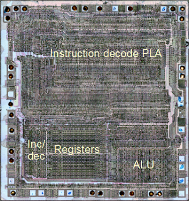
I have been reverse-engineering the Z-80 processor using images from the Visual 6502 team. The image below shows the overall structure of the Z-80 chip and the location of the ALU. The remainder of this article dives into the details of the ALU: its architecture, how it works, and exactly how it is implemented.

I've created the following block diagram to give an overview of the structure of the Z-80's ALU. Unlike Z-80 block diagrams published elsewhere, this block diagram is based on the actual silicon. The ALU consists of 4 single-bit units that are stacked to form a 4-bit ALU. At the left of the diagram, the register bus provides the ALU's connection to the register file and the rest of the CPU.

The operation of the ALU starts by loading two 8-bit operands from registers into internal latches. The ALU does a computation on the low 4 bits of the operands and stores the result internally in latches. Next the ALU processes the high 4 bits of the operands. Finally, the ALU writes the 8 bits of result (the 4 low bits from the latch, and the 4 high bits just computed) back to the registers. Thus, by doing two computation cycles, the ALU is able to process a full 8 bits of data. ("Full 8 bits" may not sound like much if you're reading this on a 64-bit processor, but it was plenty at the time.)

As the block diagram shows, the ALU has two internal 4-bit buses connected to the 8-bit register bus: the low bus provides access to bits 0, 1, 2, and 3 of registers, while the high bus provides access to bits 4, 5, 6, and 7. The ALU uses latches to store the operands until it can use them. The op1 latches hold the first operand, and the op2 latches hold the second operand. Each operand has 4 bits of low latch and 4 bits of high latch, to store 8 bits.

Multiplexers select which data is used for the computation. The op1 latches are connected to a multiplexer that selects either the low or high four bits. The op2 latches are connected to a multiplexer that selects either the low or high four bits, as well as selecting either the value or the inverted value. The inverted value is used for subtraction, negation, and comparison.

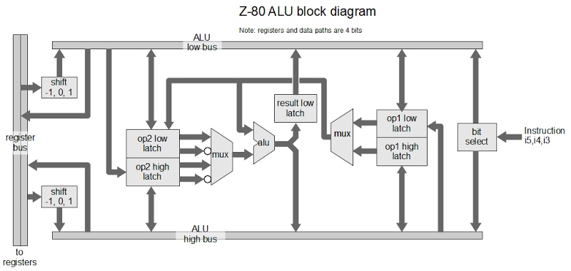
The two operands go to the "alu core", which performs the desired operation: addition, logical AND, logical OR, or logical XOR. The ALU first performs one computation on the low bits, storing the 4-bit result into the result low latch. The ALU then performs a second computation on the high bits, writing the latched low result and the freshly-computed high bits back to the bus. The carry from the first computation is used in the second computation if needed.

The Z-80 provides extensive bit-addressed operations, allowing a single bit in a byte to be set, reset, or tested. In a bit-addressed operation, bits 5, 4, and 3 of the instruction select which of the 8 bits to use. On the far right of the ALU block diagram is the bit select circuit that support these operations. In this circuit, simple logic gates select one of eight bits based on the instruction. The 8-bit result is written to the ALU bus, where it is used for the bit-addressed operation. Thus, decoding this part of an instruction happens right at the ALU, rather than in the regular instruction decode logic.

The Z-80's shift circuitry is interesting. The 6502 and 8085 have an additional ALU operation for shift right, and perform shift left by adding the number to itself. The Z-80 in comparison performs a shift while loading a value into the ALU. While the Z-80 reads a value from the register bus, the shift circuit selects which lines from the register bus to use. The circuit loads the value unchanged, shifted left one bit, or shifted right one bit. Values shifted in to bit 0 and 7 are handled separately, since they depend on the specific instruction.

The block diagram also shows a path from the low bus to the high op2 latch, and from the high bus to the low op1 latch. These are for the 4-bit BCD shifts RRD and RLD, which rotate a 4-bit digit in the accumulator with two digits in memory.

Not shown in the block diagram are the simple circuits to compute parity, test for zero, and check if a 4-bit value is less than 10. These values are used to set the condition flags.

The silicon that implements the ALU

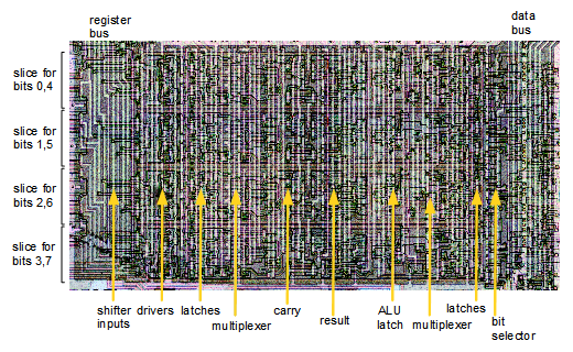
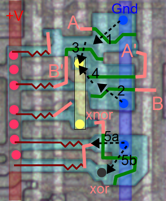
The image above zooms in on the ALU region of the Z-80 chip. The four horizontal "slices" are visible. The organization of each slice approximately matches the block diagram. The register bus is visible on the left, running vertically with the shifter inputs sticking out from the ALU like "fingers" to obtain the desired bits. The data bus is visible on the right, also running vertically. The horizontal ALU low and ALU high lines are visible at the top and bottom of each slice. The yellow arrows show the locations of some ALU components in one of the slices, but the individual circuits of the ALU are not distinguishable at this scale. In a separate article, I zoom in to some individual gates in the ALU and show how they work: Reverse-engineering the Z-80: the silicon for two interesting gates explained.

The ALU's core computation circuit

The silicon that implements one bit of ALU processing

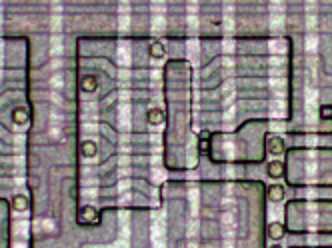
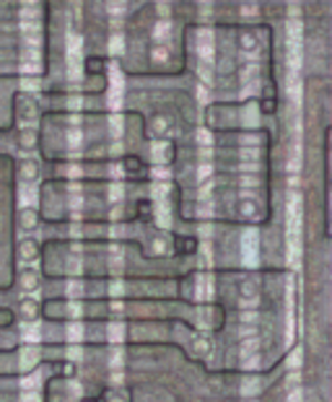
The heart of each bit of the ALU is a circuit that computes the sum, AND, OR, or XOR for two one-bit operands. Zooming in shows the silicon that implements this circuit; at this scale the transistors and connections that make up the gates are visible. Power, ground, and the control lines are the vertical metal stripes. The shiny horizontal bands are polysilicon "wires" which form the connections in the circuit as well as the transistors. I know this looks like mysterious gray lines, but by examining it methodically, you can figure out the underlying circuit. (For details on how to figure out the logic from this silicon, see my article on the Z-80's gates.) The circuit is shown in the schematic below.

The Z-80 ALU circuit that computes one bit

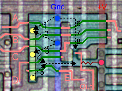
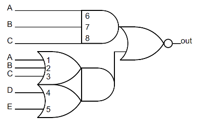
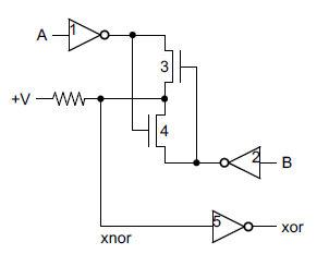
This circuit takes two operands (op1 and op2), and a carry in. It performs an operation (selected by control lines R, S, and V) and generates an internal carry, a carry-out, and the result.

ALU computation logic in detail

The first step is the "carry computation", which is done by one big multi-level gate. It takes the two operand bits (op1 and op2) and the carry in, and computes the (complemented) internal carry that results from adding op1 plus op2 plus carry-in. There are just two ways this sum can cause a carry: if op1 and op2 are both 1 (bottom AND gate); or if there's a carry-in and at least one of the operands is a 1 (top gates). These two possibilities are combined in the NOR gate to yield the (complemented) internal carry. The internal carry is inverted by the NOR gate at the bottom to yield the carry out, which is the carry in for the next bit. There are a couple control lines that complicate carry generation slightly. If S is 1, the internal carry will be forced to 0. If R is 1, the carry out will be forced to 0 (and thus the carry in for the next bit).

The multi-level result computation gate is interesting as it computes the SUM, XOR, AND or OR. It takes some work to step through the different cases, but if anyone wants the details:

  • SUM: If R is 0, S is 0, and V is 0, then the circuit generates the 1's bit of op1 plus op2 plus carry-in, i.e. op1 xor op2 xor carry-in. To see this, the output is 1 if all three of op1, op2, and carry-in are set, or if at least one is set and there's no internal carry (i.e. exactly one is set).
  • XOR: If R is 1, S is 0, and V is 0, then the circuit generates op1 xor op2 To see this, note that this is like the previous case except carry-in is 0 because of R.
  • AND: If R is 0, S is 1, and V is 0, then the circuit generates op1 and op2. To see this, first note the internal carry is forced to 0, so the lower AND gate can never be active. The carry-in is forced to 1, so the result is generated by the upper AND gate.
  • OR: If R is 1, S is 1, and V is 1, then the circuit generates op1 or op2. The internal carry is forced to 0 by S and the the carry-out (carry-in) is forced to 0 by R. Thus, the top AND gate is disabled, and the 3-input OR gate controls the result.

Believe it or not, this is conceptually a lot simpler than the 8085's ALU, which I described in detail earlier. It's harder to understand, though, then the 6502's ALU, which uses simple gates to compute the AND, OR, SUM, and XOR in parallel, and then selects the desired result with pass transistors.

Conclusion

The Z-80's ALU is significantly different from the 6502 or 8085's ALU. The biggest difference is the 6502 and 8085 use 8-bit ALUs, while the Z-80 uses a 4-bit ALU. The Z-80 supports bit-addressed operations, which the 6502 and 8085 do not. The Z-80's BCD support is more advanced than the 8085's decimal adjust, since the Z-80 handles addition and subtraction, while the 8085 only handles addition. But the 6502 has more advanced BCD support with a decimal mode flag and fast, patented BCD logic.

If you've designed an ALU as part of a college class, it's interesting to compare an "academic" ALU with the highly-optimized ALU used in a real chip. It's interesting to see the short-cuts and tradeoffs that real chips use.

I've created a more detailed schematic of the Z-80 ALU that expands on the block diagram and the core schematic above and shows the gates and transistors that make up the ALU.

I hope this exploration into the Z-80 has convinced you that even with a 4-bit ALU, the Z-80 could still do 8-bit operations. You didn't get ripped off on your old TRS-80.

Credits: This couldn't have been done without the Visual 6502 team especially Chris Smith, Ed Spittles, Pavel Zima, Phil Mainwaring, and Julien Oster.

Intel x86 documentation has more pages than the 6502 has transistors

Microprocessors have become immensely more complex thanks to Moore's Law, but one thing that has been lost is the ability to fully understand them. The 6502 microprocessor was simple enough that its instruction set could almost be memorized. But now processors are so complex that understanding their architecture and instruction set even at a superficial level is a huge task. I've been reverse-engineering parts of the 6502, and with some work you can understand the role of each transistor in the 6502. After studying the x86 instruction set, I started wondering which was bigger: the number of transistors in the 6502 or the number of pages of documentation for the x86.

It turns out that Intel's Intel® 64 and IA-32 Architectures Software Developer Manuals (2011) have 4181 pages in total, while the 6502 has 3510 transistors. There are actually more pages of documentation for the x86 than the number of individual transistors in the 6502.

The above photo shows Intel's IA-32 software developer's manuals from 2004 on top of the 6502 chip's schematic. Since then the manuals have expanded to 7 volumes.

The 6502 has 3510 transistors, or 4528, or 6630, or maybe 9000?

As a slight tangent, it's actually hard to define the transistor count of a chip. The 6502 is usually reported as having 3510 transistors. This comes from the Visual 6502 team, which dissolved a 6502 chip in acid, photographed the die (below), traced every transistor in the image, and built a transistor-level simulator that runs 6502 code (which you really should try). Their number is 3510 transistors.

The 6502 processor chip

One complication is the 6502 is built with NMOS logic which builds gates out of active "enhancement" transistors as well as pull-up "depletion" transistors which basically act as resistors. The count of 3510 is just the enhancement transistors. If you include the 2102 1018 depletion transistors, the total transistor count is 5612 4528.

A second complication is that when manufacturers report the transistor count of chips, they often report "potential" transistors. Chips that include a ROM or PLA will have different numbers of transistors depending on the values stored in the ROM. Since marketing doesn't want to publish different transistor numbers depending on the number of 1 bits and 0 bits programmed into the chip, they often count ROM or PLA sites: places that could have transistors, but might not. By my count, the 6502 decode PLA has 21×131=2751 PLA sites, of which 649 actually have transistors. Adding these 2102 "potential" transistors yields a count of 6630 transistors.

Finally, some sources such as Microsoft Encarta and A History of the Personal Computer state the 6502 contains 9000 transistors, but I don't know how they could have come up with that value.

(The number of pages of Intel documentation is also not constant; the latest 2013 Software Developer Manuals have shrunk to 3251 pages.)

Thus, the x86 has more pages of documentation than the 6502 has transistors, but it depends how you count.

Reverse-engineering the Z-80: the silicon for two interesting gates explained

I've been reverse-engineering the Z-80 processor, using images from the Visual 6502 team. One interesting thing about the Z-80's silicon is it uses complex gates with multiple inputs and multiple levels of logic. It also implements an XOR gate with an unusual pass-transistor circuit. I thought it would be interesting to examine these gates at the silicon level and show how they work.

The image above shows the overall organization of the Z-80 chip. I'm going to zoom way in on the ALU and look at the silicon that implements one of the complex gates there: a 5-input, three-level gate. I'll walk through this gate and show how it works at the silicon level. While the silicon look like a jumble of lines, its operation is actually straightforward if you step through it.

Let's begin with an (oversimplified) description of how the chip is constructed. The chip starts with the silicon wafer. Regions are diffused with an element such as boron, yielding conductive diffusion regions. A layer of polysilicon strips is put on top. Finally, a layer of metal "wires" above the polysilicon provides more connections. For our purposes, diffusion regions, polysilicon, and metal can all be consider conductors.

In the image below, the bright vertical bands are metal wires. The slightly darker horizontal bands are polysilicon; the borders are more visible than the regions themselves. In this part of the Z-80, the polysilicon connections run mostly horizontally, and the metal wires run vertically. The large irregular regions outlined in black are doped silicon diffusion regions. The circles are vias between different layers.

Transistors are formed where a polysilicon line crosses a diffusion region. You might expect transistors to be very visible in the image, but a polysilicon line looks the same whether its a conductor or a transistor. So transistors just appear as long skinny regions in the image. The diagram below shows the physical structure of a transistor: the source and drain are connected if the gate is positive.

Structure of an NMOS transistor

Let's dive in and see how this circuit works. There's a lot going on, but the image below has been colored to make it clearer. Only three of the vertical metal lines are relevant. On the left, the yellow metal line ties together parts of the gate. In the middle is the blue ground line, which is critical to the operation of the gate. At the right, the red positive voltage line is used to pull the output high through a resistor. The large diffusion region has been tinted cyan. This region can be thought of as big conductive areas interrupted by transistors. There are 5 pinkish polysilicon input wires, labeled A, B, C, D, E. When they cross the diffusion region they still act as wires, but also form a transistor below in the diffusion region. For instance, input A is connected to two transistors.

With all the pieces labeled, we can figure out the operation of the circuit. If input A is high, the first transistor will conduct and connect the yellow strip to ground (dotted line 1). Likewise, if input B is high, the second transistor will conduct and ground the yellow strip (dotted line 2). C will ground the yellow strip via 3. So the yellow strip will be grounded for A or B or C. This forms a three-input OR gate.

If input D is high, transistor 4 will connect the yellow strip to the output. Likewise, if input E is high, transistor 5 will connect the yellow strip to the output. Thus, the output will be grounded if (A or B or C) and (D or E).

In the upper right, arrow 6/7/8 will ground the output if A and B and C are high and the three associated transistors (6, 7, 8) conduct. This computes A and B and C.

Putting this all together, the output will be grounded if [(A or B or C) and (D or E)] or [A and B and C]. If the output is not grounded, the resistor (actually a depletion transistor) will pull the output high. Thus, the final output is not [(A or B or C) and (D or E)] or [A and B and C].

The diagram below shows the gate logic implemented by this circuit. This rather complex gate is created from just nine transistors. Note that the final AND and NOR gates are "for free" - they are formed by wiring together previous outputs and don't require additional transistors. Another point of interest is that with NMOS, the output will be high unless something pulls it low, which explains why circuits are based on NAND and NOR gates rather than AND and OR gates.

If you want to see more low-level silicon analysis, see my article on the overflow circuit in the 6502 at the silicon level.

What does this gate do?

This gate is a key part of one bit of the Z-80's ALU. The gate generates the (inverted) sum, AND, OR, or XOR of B and C depending on the inputs. Specifically, B and C are the two operand inputs, and A is the carry in. D is a control input and E is an inverted intermediate carry from B plus C plus carry_in. By controlling D and overriding A and E, the operation is selected.

The Z-80's interesting XOR gate

The Z-80 uses an unusual circuit for its XOR gate. XOR is an inconvenient function to implement since it has a worst-case Karnaugh map, making it expensive to implement from simple gates. Instead, the Z-80 uses a combination of inverters and pass transistors, different from regular NMOS logic.

As before, the diagram below shows the power and ground metal lines, a connecting metal line in yellow, the polysilicon in pink, the polysilicon transistor gates in green, and diffusion in cyan. The two inputs are A and B.

Starting with input A: if it is high, transistor 1 will connect A' to ground. Otherwise the pullup resistor (way on the left), will pull A' high. (Note that A' is the whole diffusion region between transistor 1 and transistor 3 up to the resistor.) Thus transistor 1 forms a simple inverter with inverted output A'. Likewise, transistor 2 inverts input B to give inverted B' (in the whole diffusion region between transistors 2 and 4).

Now comes the tricky part. If A' is high, pass transistor 4 will connect B' to the yellow metal. If B' is high, pass transistor 3 will connect A' to the yellow metal. The third pullup resistor will pull the yellow metal high unless something ties it to ground . Working through the combinations, if A' and B' are both high, both A' and B' are connected to the yellow metal, which gets pulled high. If A' is high and B' is low, B' is connected to the yellow metal, pulling it low. Likewise, if A' is low and B' is high, A' pulls the yellow metal low. Finally if A' and B' are low, nothing gets connected to the yellow metal, so the resistor pulls it high.

To summarize, the yellow metal is pulled high if A' and B' are both high or both low. That is, it is the exclusive-nor of A' and B', which is also the exclusive-or of A and B.

Finally, the xnor value controls transistors 5a and 5b which form an inverter. If xnor is high, transistors 5a and 5b conduct and the xor output is connected to ground, and if xnor is low, the pullup resistors pull the xor output high. One unusual feature here is the parallel transistors 5a and 5b with separate pullup resistors. I haven't seen this in the 8085 or 6502; they use a single larger transistor instead of parallel transistors.

The schematic below summarizes the circuit. In case you're wondering, this XOR gate is used to compute the parity flag. All the bits are XORed together to generate the parity flag.

Comparison to other processors

From what I've seen so far, the Z-80 uses considerably more complex gates than the 8085 and the 6502. The 6502 uses mostly simple NAND/NOR gates and only a few two-level gates, not as complex as on the Z-80. The 8085 uses more complex gates, but still less than the Z-80. I don't know if the difference is due to technical limits on the number of gate levels, or the preferences of the designers.

The XOR circuit in the Z-80 is different from the 8085 and 6502. I'm not sure it saves any transistors, but it is unusual. I've seen other pass-transistor implementations of XOR, but none like the Z-80.

Credits: The Visual 6502 team especially Chris Smith, Ed Spittles, Pavel Zima, Phil Mainwaring, and Julien Oster.

9 Hacker News comments I'm tired of seeing

As a long-time reader of Hacker News, I keep seeing some comments they don't really contribute to the conversation. Since the discussions are one of the most interesting parts of the site I offer my suggestions for improving quality.
  • Correlation is not causation: the few readers who don't know this already won't benefit from mentioning it. If there's some specific reason you think a a study is wrong, describe it.
  • "If you're not paying for it, you're the product" - That was insightful the first time, but doesn't need to be posted about every free website.
  • Explaining a company's actions by "the legal duty to maximize shareholder value" - Since this can be used to explain any action by a company, it explains nothing. Not to mention the validity of the statement is controversial.
  • [citation needed] - This isn't Wikipedia, so skip the passive-aggressive comments. If you think something's wrong, explain why.
  • Premature optimization - labeling every optimization with this vaguely Freudian phrase doesn't make you the next Knuth. Calling every abstraction a leaky abstraction isn't useful either.
  • Dunning-Kruger effect - an overused explanation and criticism.
  • Betteridge's law of headlines - this comment doesn't need to appear every time a title ends in a question mark.
  • A link to a logical fallacy, such as ad hominem or more pretentiously tu quoque - this isn't a debate team and you don't score points for this.
  • "Cue the ...", "FTFY", "This.", "+1", "Sigh", "Meh", and other generic internet comments are just annoying.
My readers had a bunch of good suggestions. Here are a few:
  • The plural of anecdote is not data
  • Cargo cult
  • Comments starting with "No." "Wrong." or "False."
  • Just use bootstrap / heroku / nodejs / Haskell / Arduino.
  • "How [or Why] did this make the front page of HN?" followed by http://ycombinator.com/newsguidelines.html
In general if a comment could fit on a bumper sticker or is simply a link to a Wikipedia page or is almost a Hacker News meme, it's probably not useful.

What comments bother you the most?

Check out the long discussion at Hacker News. Thanks for visiting, HN readers!

Amusing note: when I saw the comments below, I almost started deleting them thinking "These are the stupidest comments I've seen in a long time". Then I realized I'd asked for them :-)

Edit: since this is getting a lot of attention, I'll add my "big theory" of Internet discussions.

There are three basic types of online participants: "watercooler", "scientific conference", and "debate team". In "watercooler", the participants are having an entertaining conversation and sharing anecdotes. In "scientific conference", the participants are trying to increase knowledge and solve problems. In "debate team", the participants are trying to prove their point is right.

HN was originally largely in the "scientific conference" mode, with very smart people discussing areas in which they were experts. Now HN has much more "watercooler" flavor, with smart people chatting about random things they often know little about. And certain subjects (e.g. economics, Apple, sexism, piracy) bring out the "debate team" commenters. Any of the three types can carry on happily by themself. However, much of the problem comes when the types of conversation mix. The "watercooler" conversations will annoy the "scientific conference" readers, since half of what they say is wrong. Conversely, the "scientific conference" commenters come across as pedantic when they interrupt a fun conversation with facts and corrections. A conversation between "debate team" and one of the other groups obviously goes nowhere.