IBM paperweight teardown: Reverse-engineering 1970s memory chips

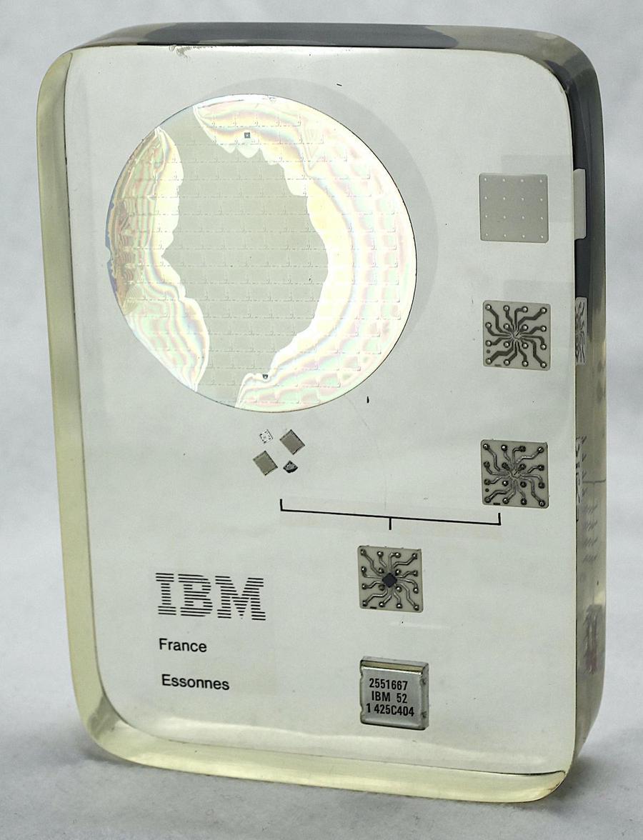
I recently received a vintage IBM paperweight from the early 1970s that showcases some memory chips.1 When IBM started using integrated circuits in the late 1960s, they packed the chips in square metal modules called Monolithic Systems Technology (MST). The paperweight illustrates the manufacturing steps for an MST module as a silicon wafer was cut into silicon dies, mounted on a square ceramic substrate, and wrapped in a thumbnail-sized metal package.

The paperweight contains a silicon wafer, four dies, and an MST module in various stages of assembly. The paperweight is somewhat yellowed with age. Click this image, or any other, for a larger photo.

The paperweight contains a silicon wafer, four dies, and an MST module in various stages of assembly. The paperweight is somewhat yellowed with age. Click this image, or any other, for a larger photo.

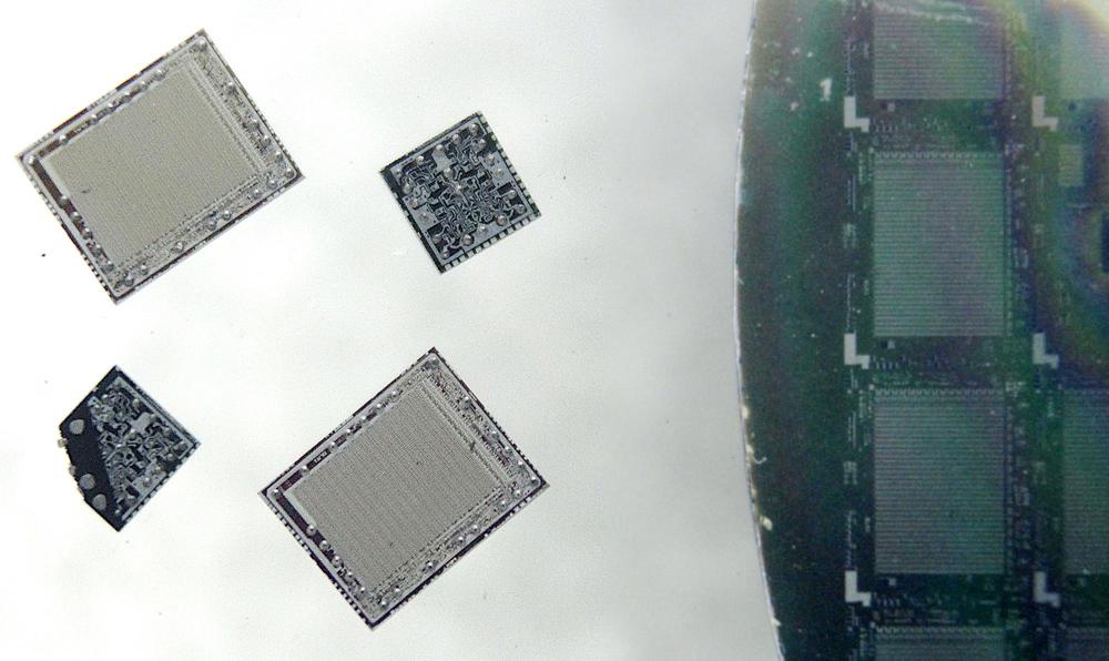
Because the dies are encased in clear Lucite, it's possible to closely examine their circuitry and understand them better. The photo below is a closeup of the edge of the silicon wafer and the four dies inside the paperweight. The two larger dies are the same as the dies on the wafer. The two smaller dies are the same, but one is visibly damaged.2 For this blog post, I took detailed die photos using a microscope and reverse-engineered the smaller chip. My conclusion is that the larger chips are 1-kilobit static RAM chips, while the smaller ones are memory sense amplifiers.

Closeup of the dies and wafer inside the paperweight.

Closeup of the dies and wafer inside the paperweight.

IBM System/370

These chips were probably used in IBM's popular System/370 line of mainframe computers. In 1964, IBM introduced the extremely successful System/360 family of mainframes. This product line was modernized in 1970 with the announcement of System/370, which was constructed from integrated circuits (unlike the System/360) and moved from magnetic core memory to semiconductor memory. The paperweight illustrates both of these changes: integrated circuits and semiconductor memory.

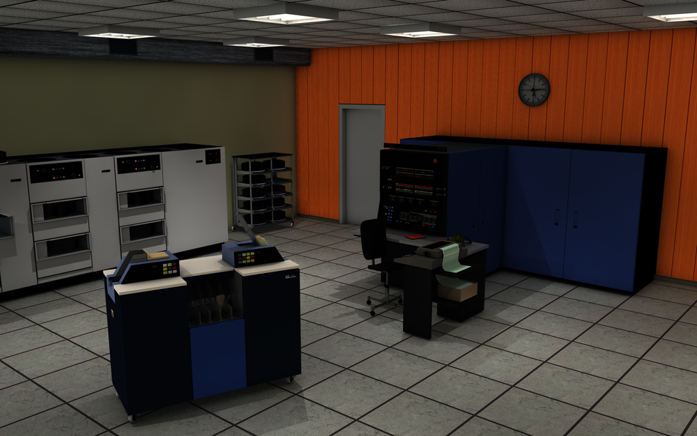
To understand the scale of a System/370 computer, the rendering below shows a System/370 Model 145. The Model 145 was a "medium-scale" machine in the middle of the System/370 family.3 The Model 145 is notable as IBM's first computer that used semiconductor main memory. The computer is very large by modern standards, filling the blue cabinets below. One cabinet holds the CPU while another holds 256 kilobytes of memory chips. This computer predates the microprocessor, so the CPU is built gate-by-gate from many boards of integrated circuits. The Model 145 weighed over a ton, cost $5 to 10 million (in current dollars), and was roughly as fast as an IBM PC (1981).

Rendering of a System/370 Model 145. The computer is the large blue cabinet along the wall. The white unit at the back is disk storage, while a card reader is in the foreground. Image by Oliver.obi, CC BY-SA 3.0.

Rendering of a System/370 Model 145. The computer is the large blue cabinet along the wall. The white unit at the back is disk storage, while a card reader is in the foreground. Image by Oliver.obi, CC BY-SA 3.0.

The MST modules

In the earlier System/360, IBM didn't use integrated circuits, but instead used hybrid modules called SLT. For the System/370 IBM moved to integrated circuits, which they called "monolithics". While most companies packaged integrated circuits in rectangular plastic or ceramic packages, IBM retained the half-inch-square metal packages of SLT, calling it MST, for Monolithic Systems Technology.4 MST was a big improvement over the earlier hybrid SLT, about ten times more reliable and 4 to 8 times as dense. These MST integrated circuits were very simple by modern standards, with 32 transistors per module implementing about six gates, so thousands of integrated circuits were required to implement the computer.

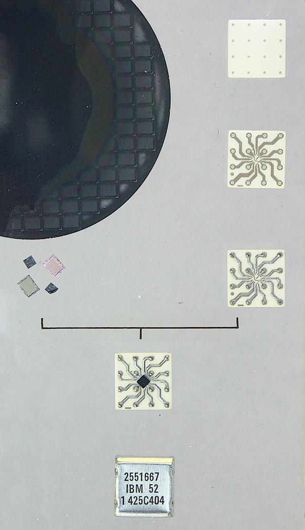
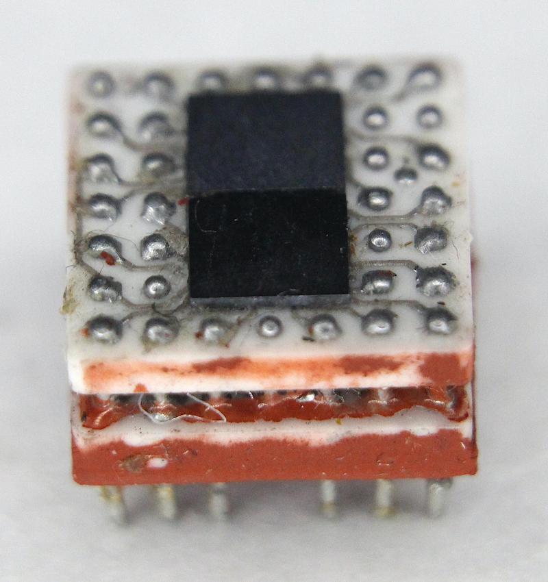
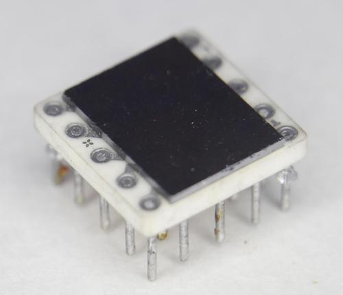
The MST modules were manufactured in large quantities with automated production techniques. The sequence of components in the paperweight (below) illustrates the steps. On the left, the round silicon wafer is cut into individual dies. On the right, the square ceramic substrate has 16 holes for pins. Next, a printed-circuit pattern is applied to the substrate to connect the integrated circuit to the module's pins.5 In the third step, 16 pins are soldered to the substrate. Next, the silicon die and the ceramic substrate are combined, with the silicon die is mounted upside-down in the center of the ceramic substrate. Note how small the silicon die is, compared to the size of the package. The module is reflow-soldered, with contacts on the silicon die soldered directly to the substrate.6 Finally, the module is encased in metal, producing a half-inch square module. These modules give IBM's integrated circuits a unique appearance, distinct from the plastic or ceramic DIP integrated circuits used by other manufacturers.

The steps to manufacture an MST module.

The steps to manufacture an MST module.

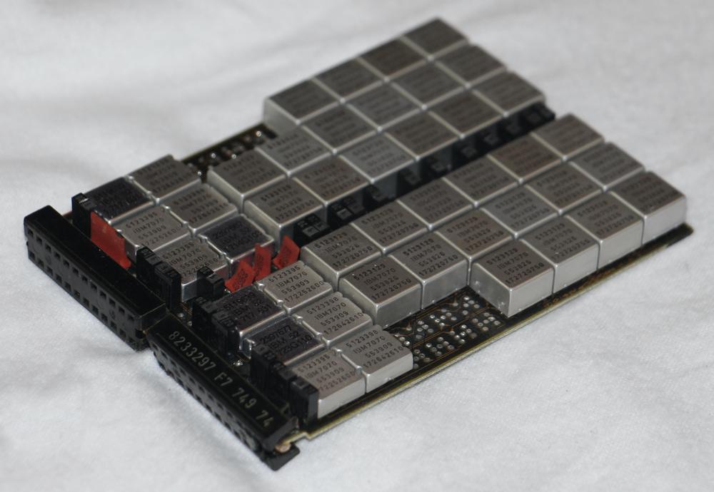
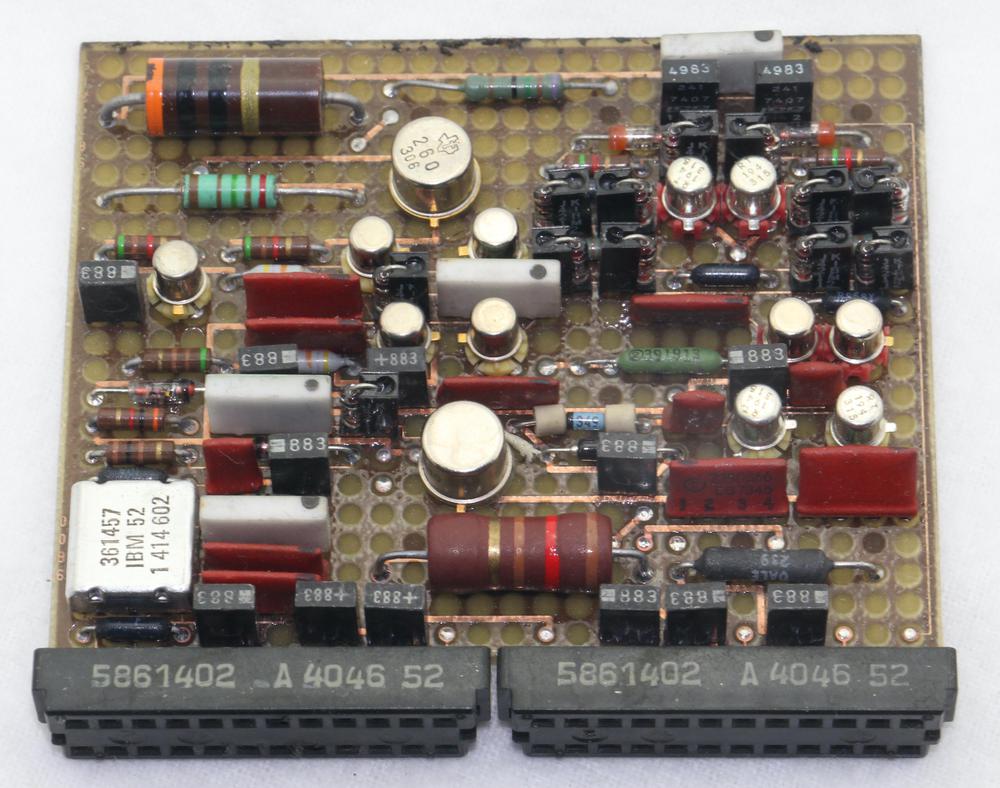
The MST modules were tightly packed on circuit cards, such as the memory card below. The square module in combination with a four-plane printed circuit board provides considerably higher density than the circuit boards of other manufacturers at the time, which typically used DIP integrated circuits and 2-layer PCBs.

An IBM memory card packed with MST modules.

An IBM memory card packed with MST modules.

The memory wafer and chip

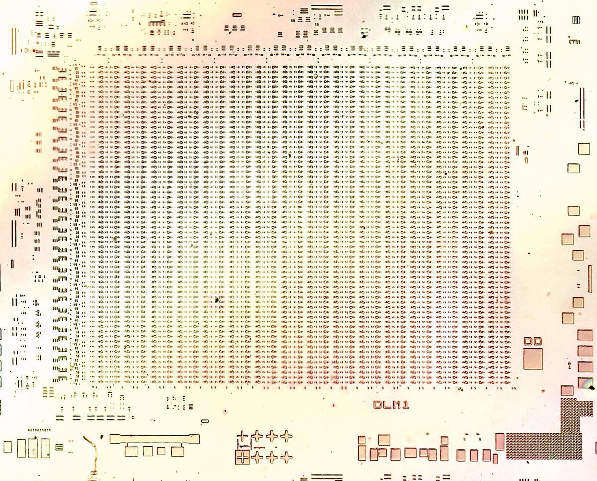
The silicon wafer in the paperweight is 2 inches in diameter, a size that was introduced in 1969. Wafer sizes have steadily increased since then and modern chip fabrication is done with much larger 300 mm (12") wafers.7 The wafer contains 177 dies; using a microscope, I created the die photo below of one of them. Curiously, the wafer is only partially manufactured; it looks like only one of the nine mask layers was constructed. Because this photo is taken from the wafer, you can see the test circuitry and alignment patterns in between the dies.

Die photo of one of the memory chips on the wafer. It is only partially manufactured. The part number "DLM1" is visible on it.

Die photo of one of the memory chips on the wafer. It is only partially manufactured. The part number "DLM1" is visible on it.

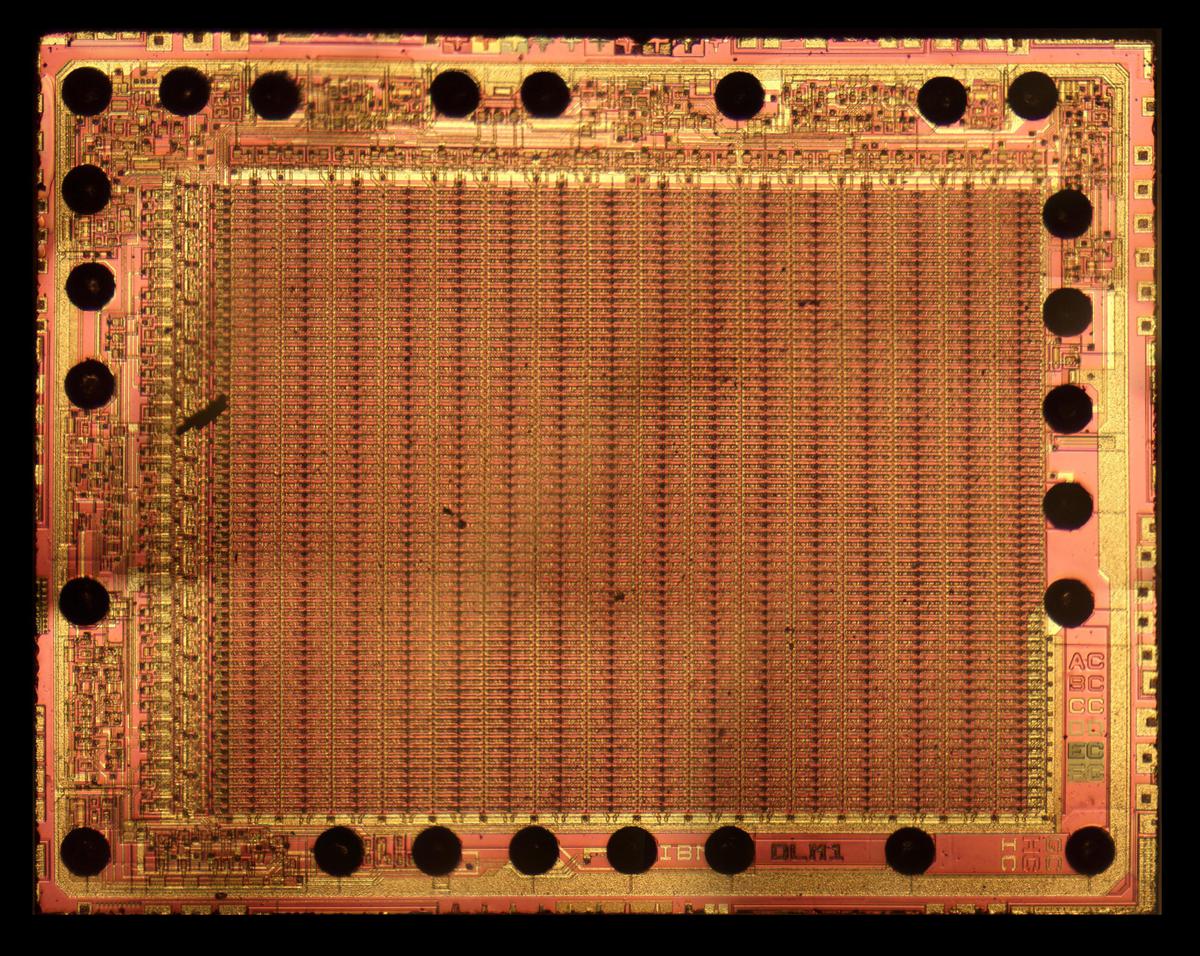
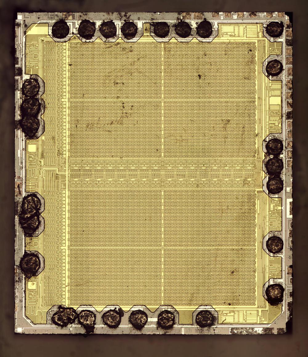
The paperweight also contains completed individual dies so I created the die photo below. The regular grid of memory cells is visible in the middle of the chip, with support circuitry around the edge. From studying the die and counting the cells, I think this is a 1-kilobit static RAM chip. Note the solder balls around the edge of the die, which allowed the chip to be soldered directly to the ceramic substrate. With 25 solder balls, this chip was probably mounted in an MST package with a 5×5 grid of pins.

Die photo of the memory chip.

Die photo of the memory chip.

Taking microscope photos is difficult when the die is encased in Lucite, so I wasn't able to see the circuitry under high magnification. As a result, I couldn't reverse-engineer this chip in detail.8 I was able to measure the feature size on the die as about 6µm, a process introduced around 1971.

The sense amplifier chip

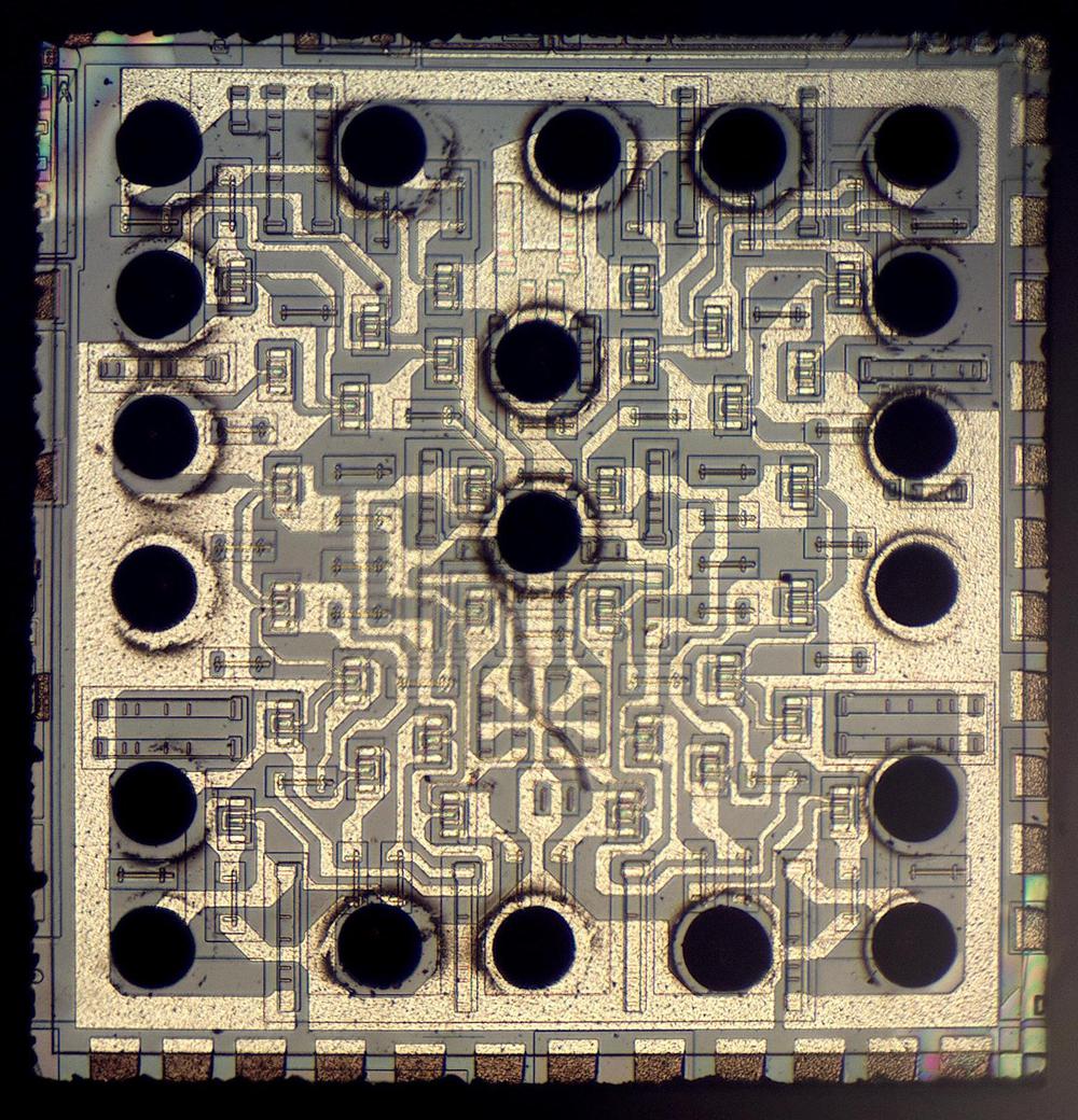
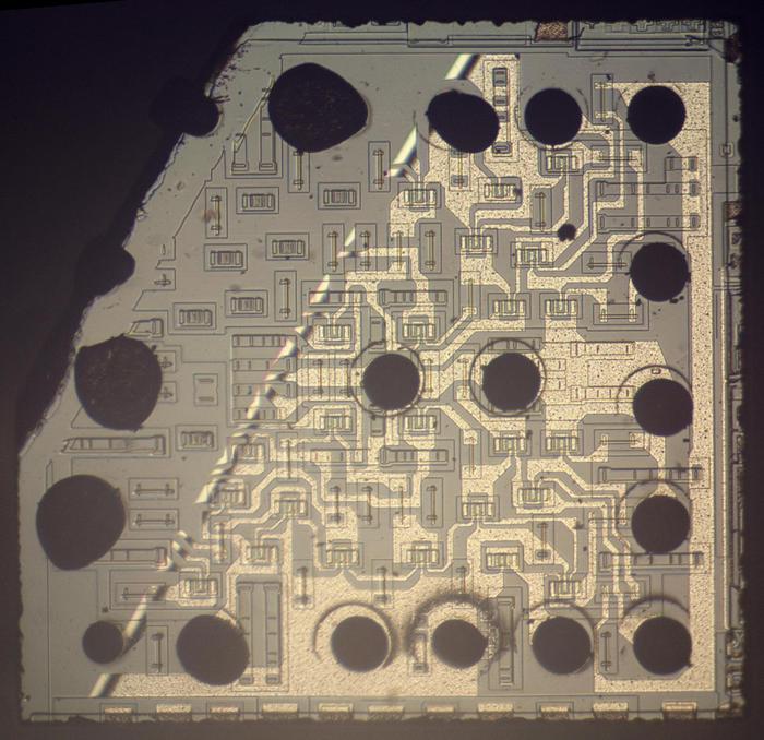
The smaller die in the paperweight is much simpler with much larger components. I took the die photo below and found it contains 32 NPN transistors along with resistors. This chip is partially analog and also uses a type of logic called ECL. I believe the chip is a differential amplifier, a sense amplifier to read the signals from the memory chip. This would explain why the two chips are packaged together in the paperweight.

Die photo of the bipolar integrated circuit. The left and right sides are approximately mirror-images, with two copies of the same circuit.

Die photo of the bipolar integrated circuit. The left and right sides are approximately mirror-images, with two copies of the same circuit.

In the die photo above, the silicon of the die is gray. Parts of the silicon were doped with arsenic, boron, or phosphorus to create regions with different semiconductor properties. The black lines in the silicon are boundaries between different doping levels. The yellowish regions are metal wiring on top of the silicon, connecting the various components together. The large black circles are the solder balls to connect the die to the MST substrate.

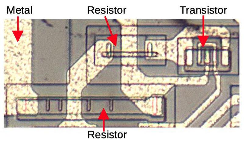
The diagram below is a detail from the chip, showing two types of resistors and a transistor. The upper resistor above is made from a line of higher-resistance N-type silicon, with metal contacts connected to either end. This forms a 65Ω resistor. The lower resistor has six contacts, providing multiple resistance values depending on where the metal lines are attached. It uses P-type silicon for the resistive element, providing hundreds of ohms of resistance. (There's a bit more internal structure to the resistors, but I'll ignore it.)

Two resistors and a transistor as they appear on the die.

Two resistors and a transistor as they appear on the die.

The transistors are bipolar NPN transistors, but their structure is a bit more complex than the typical NPN transistor. Physically, they have two bases and two collectors wired together to reduce current density, so you'll see five metal connections to each transistor. The diagram below shows the cross-section structure of the transistor. The five metal connections on top of the cross-section correspond to the five connections on the transistor above. The collector, base, and emitter are connected to N-P-N layers, forming the NPN transistor.9 The P+ ring provides isolation around the transistor.

This diagram shows the internal structure of the chip's transistors, based on patent 3539876.

This diagram shows the internal structure of the chip's transistors, based on patent 3539876.

By recognizing the components on the die and tracing out the wiring, the circuit can be reverse-engineered. However, if you look at the die closely, you'll see that many components are not connected. The reason is that IBM used a technique called "master slice" to produce a variety of integrated circuits without custom-designing each one.10 The idea was to use a common silicon die with multiple transistors and resistors. By modifying the metal layer (which was relatively inexpensive), the components could be wired into the desired circuits. This is also why the resistors had multiple taps, so they could be wired to obtain different values as needed.

The differential amplifier and ECL logic

Logic circuits can be built in a wide variety of ways. Almost all computers today use a logic family called CMOS (complementary metal-oxide-semiconductor), building gates out of MOS transistors. However, the IBM System/370 used a high-performance11 logic family known as Emitter-coupled logic (ECL), which IBM called Current-Switch Emitter Follower (CSEF).12 ECL was invented at IBM in 1956 for use in IBM's high-performance transistorized computers.

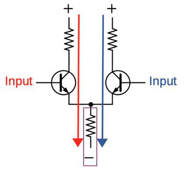
ECL is based on a differential pair, a circuit that amplifies the difference between two inputs. (This circuit is also the basis of op-amps.) The idea behind a differential pair (below) is that a fixed current flows through the circuit. If the left input is a higher voltage than the right, the left transistor will turn on and most current will flow through the left branch (red). Conversely, if the right input is a higher voltage than the left, the right transistor will turn on and most current will flow through the right branch (blue). The differential pair provides amplification because a small difference in the inputs will create a large shift in the current.

A differential pair amplifies the difference between the two inputs.

A differential pair amplifies the difference between the two inputs.

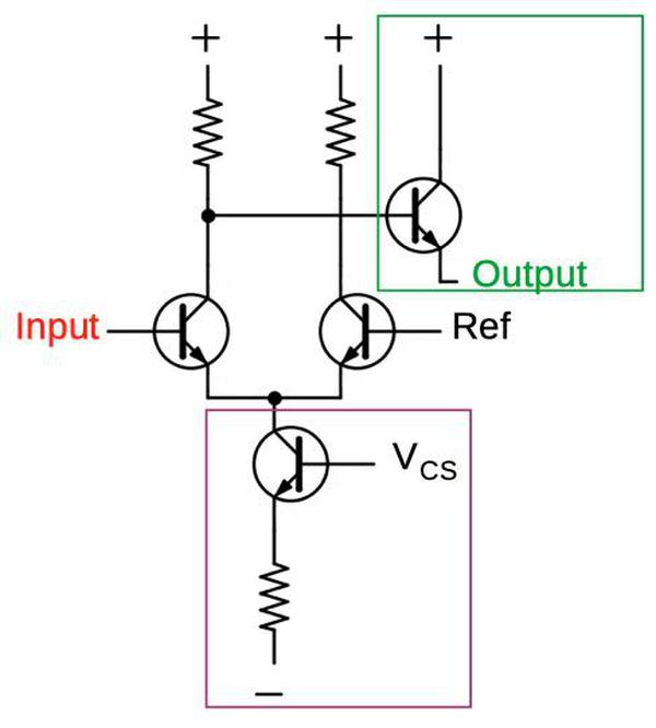
The above circuit is used as an amplifier in the chip, but with a few modifications it also forms an ECL gate. For a gate, the voltage into one branch is fixed at a reference voltage, midway between the "0" level and the "1" level. Thus, if the input is higher than the reference voltage, it will be considered a "1", and lower will be a "0". (MST chips used ground as the reference voltage.4) The ECL circuit below is an inverter, since if the input is high, the current through the left resistor will pull the output low. To improve performance, the bottom resistor has been replaced with a current sink circuit (purple). The current through the current sink is set by an external bias voltage (VCS).

The differential pair can be modified to produce an ECL inverter.

The differential pair can be modified to produce an ECL inverter.

A buffer (green) has been added to the output above. The buffer circuit is called an emitter follower since the output is taken from the transistor's emitter and the output follows the input. This is why IBM used the name Current-Switch Emitter Follower for this logic family.

The sense amplifier chip's circuitry

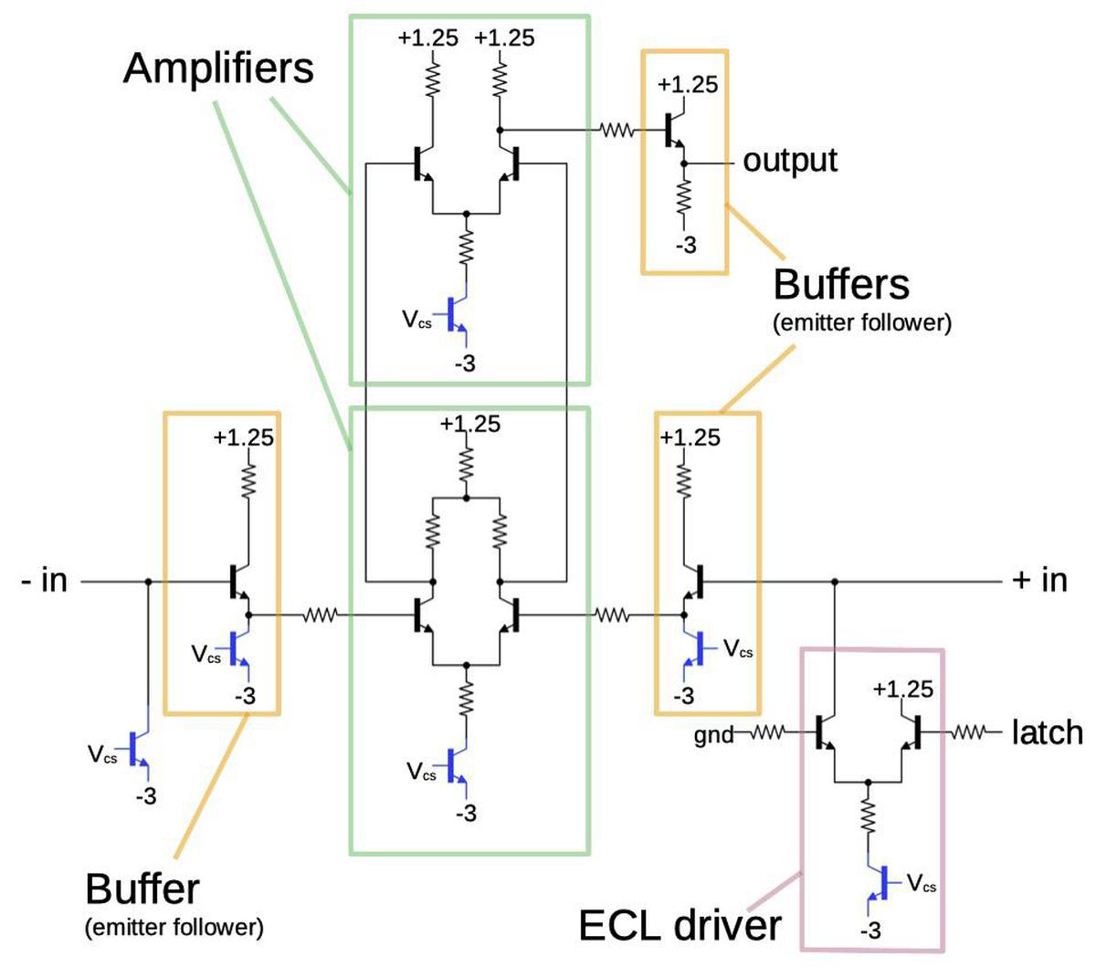
I reverse-engineered the chip's circuitry and found it contains two copies of the circuit below. This circuit is a differential amplifier, probably used as a sense amplifier to amplify the outputs from the memory chip and convert them to logic signals.13

The chip takes two inputs, a negative input and a positive input, and produces a logic-level output. The circuit is a bit complicated, but I'll try to explain the highlights. The differential amplifiers (discussed earlier) are the core of the chip. The input signals are buffered and then go into the lower amplifier (green box). The outputs from that amplifier go into the upper amplifier. Cascading two amplifier stages in this way makes the chip very sensitive, providing a large degree of amplification.

Reverse-engineered schematic of the sense amplifier chip.

Reverse-engineered schematic of the sense amplifier chip.

The yellow boxes are buffers, using the emitter-follower circuit described earlier. One buffer is used on each input and one on the output. The purple box is an ECL gate. I believe it is used to latch the amplifier's value by feeding the output back in. The current sink transistors are colored blue to distinguish them. They provide a constant current to the differential amplifiers and other circuits.

Conclusion

Well, this is a lot of analysis for a paperweight. But this paperweight provides an interesting window into IBM's technology of 1974.14 In particular, it illustrates IBM's transition to integrated circuits and semiconductor memory for the System/370 mainframes. It also explains IBM's unique construction technique for integrated circuits, packaging them on a ceramic wafer in a square metal can, a technology they called MST. Finally, the paperweight's 1-kilobit memory chip shows the amazing progress that memory technology has made over the past decades, giving us megabit chips and now multi-gigabit chips.

Thanks to @magnetic_tape for sending me the paperweight. Thanks to Mark Smotherman for information on MST. I announce my latest blog posts on Twitter, so follow me @kenshirriff. I also have an RSS feed. If you're interested in old IBM technology, see my recent post on an IBM Technology Box, covering 1948 to 1986.

Notes and references

  1. The text "Essones" on the paperweight refers to IBM's semiconductor plant in Corbeil-Essones, a suburb of Paris. IBM opened this plant in 1964, Europe's biggest semiconductor factory at the time. 

  2. Curiously, one of the dies in the paperweight is damaged and has a corner missing. Note that it's not simply broken, since the metal layer and the silicon doping don't go to the edge. Probably this die is from the edge of the wafer so it didn't get fully exposed. With the incomplete wafer and the truncated die, it's clear that they were using junk parts in the paperweights.

    One die in the paperweight is damaged.

    One die in the paperweight is damaged.


  3. For a while, IBM used a rational numbering system for the System/370 models, with computer power increasing with the model number. Model numbers ranged from the low-end Model 115 to the high-end Model 195. However, the numbering system fell apart in the late 1970s as systems were assigned seemingly-random numbers such as 3031, 4361, 3090, and 9370. Despite having the biggest number, the 9370 was a low-end machine. See IBM's 360 and Early 370 Systems for a detailed history of the System/370. 

  4. IBM had multiple versions of MST logic for different products; some versions used different voltages. MST-1 uses ground as the upper voltage, -4 volts as the lower voltage, and -1.32 volts as the ECL reference voltage. (Because ECL circuits are more sensitive to fluctuations in the upper voltage, ECL families often assign that level to ground, making the lower voltage negative.) MST-2 shifts the levels so the reference level is ground; the upper voltage is +1.25V and the lower is -3V.

    I couldn't find much information on the other MST variants, but for reference I'll summarize what I did find. MST-2 was used in the S/370 Models 145 and 155, while MST-4 was a high-performance version developed by Texas Instruments and used in the S/360 Model 85. The S/370 Model 168 used MST-1, MST-2, MST-4, and MST-A. The System/3 used MST-10. The IBM 3889 OCR machine, 3350 Disk Storage, and 3704 Communications Controller used MST-1 and MST-E. The IBM 3031 used MST-1, MST-2, MST-4, MST-4E, MST-E, and MST-A. Other versions included MST-195 and MST-255. 

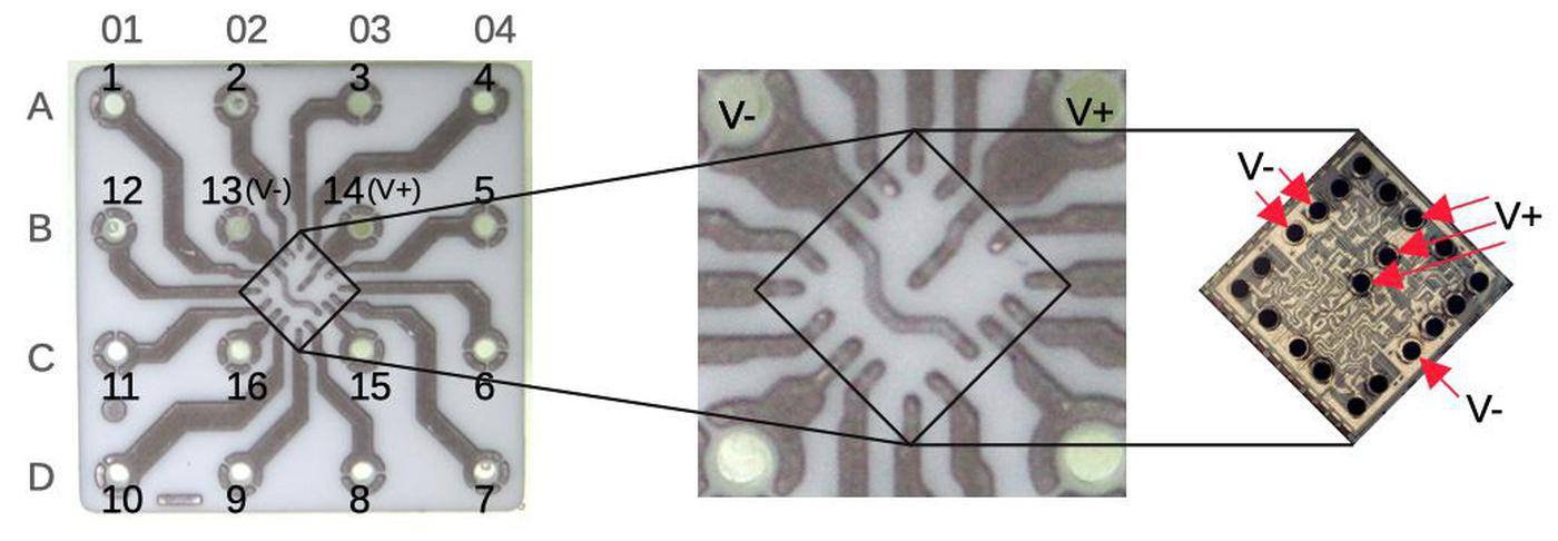
  5. The MST ceramic substrate provides the interface between two circuitry scales: the printed circuit board scale with 0.125-inch pin spacing, and the integrated circuit scale with 0.01-inch solder ball spacing. The pattern on the MST ceramic substrate has some interesting subtleties; each power pin is connected to three solder balls, allowing more current into the IC. The trace for V- crosses the chip, providing two connections on one side and on on the other. The trace for V+ extends into the middle of the IC to provide additional power connections.

    Diagram showing how the chip is mounted on the ceramic substrate. (The chip image has been mirrored to account for it being mounted upside down.)

    Diagram showing how the chip is mounted on the ceramic substrate. (The chip image has been mirrored to account for it being mounted upside down.)

    For some reason, MST uses two different pin-numbering schemes. The 12-pin SLT numbering was extended by spiraling 13-16 into the middle. But the more common MST pin names are A01 through D04.


  6. IBM called the chip mounting technique "controlled-collapse chip connections" or C-4. It used a controlled volume of solder to make electrical and mechanical contact with the module. During soldering, the chip was pulled into alignment with the module fingers by surface tension, similar to how a surface-mount device is soldered today. For more details, see Design of Logic Circuit Technology for IBM System/370 Models 145 and 155

  7. Information on wafer sizes is here and on Wikipedia

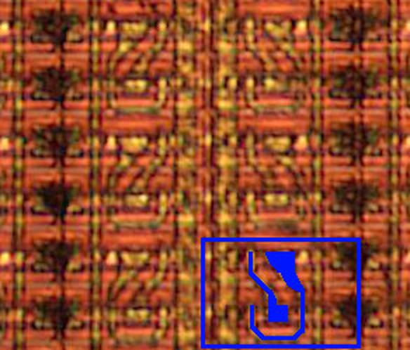
  8. The photo below is the best resolution I could get of the memory cells. I believe this is six memory cells; I put a box around one. The circuitry in two rows is connected as shown in blue. This is probably two cross-coupled inverters, a standard circuit for a static RAM cell.

    Closeup of six memory cells in the memory chip.

    Closeup of six memory cells in the memory chip.


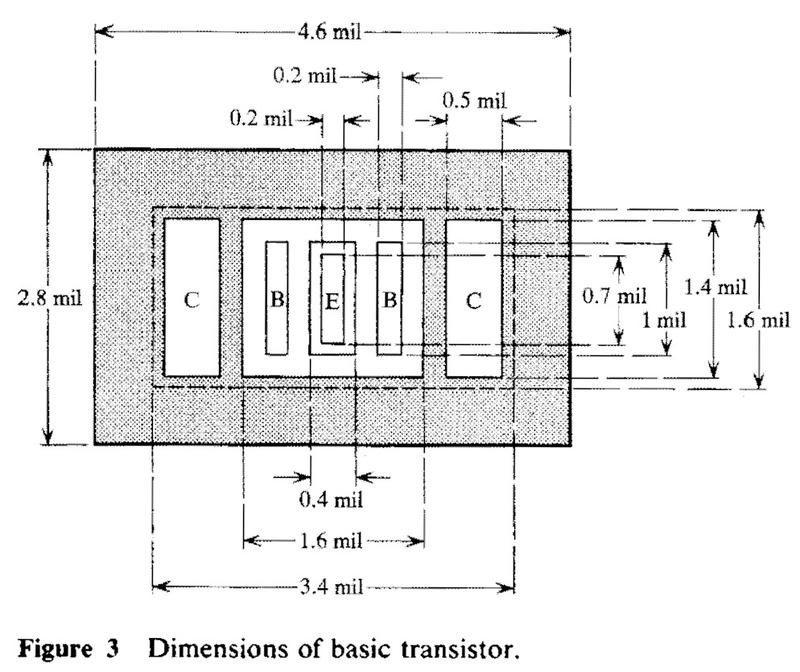
  9. The diagram below provides more details on the construction and dimensions of the transistors.

    The transistors in the MST chips have a single base and collector but has two base and collector connections to reduce current density. Image from Design of Logic Circuit Technology for IBM System/370 Models 145 and 155.

    The transistors in the MST chips have a single base and collector but has two base and collector connections to reduce current density. Image from Design of Logic Circuit Technology for IBM System/370 Models 145 and 155.


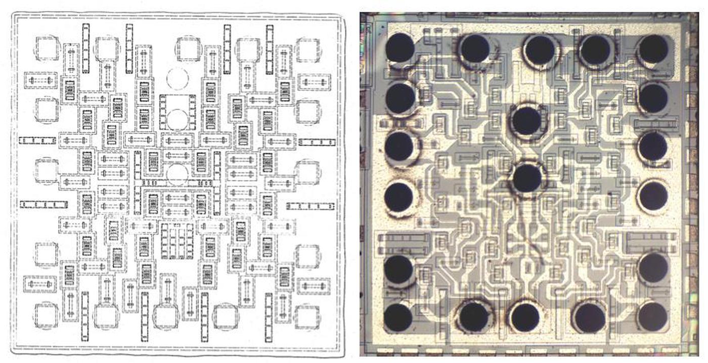
  10. The master slice approach used a fixed silicon layout with transistors and resistors, but changed the metal interconnections to create different chips, a process called "personalization". The diagram below, from patent 3539876, shows a silicon layout used for IBM's master slice integrated circuits. If you match up the resistors and transistors, this diagram is almost identical to the die in the paperweight. There are a few differences, though. In particular, the die has an extra pin on the left and right, with slight resistor changes to accommodate them. Design of Monolithic Circuit Chips (1966) describes the origins of the master slice approach. Even in 1966, they were using computer-assisted design for integrated circuits.

    The die structure from patent 3539876 is almost identical to the chip.

    The die structure from patent 3539876 is almost identical to the chip.


  11. ECL gates obtained much of their speed advantage because the transistors were not completely turned on (i.e. saturated). This allowed the transistors to switch the current path rapidly. Additionally, the difference between a "0" voltage and a "1" voltage was small (about 0.8) volts, so signals could switch between the two voltages quickly. In comparison, TTL gates typically had a difference of about 3.2 volts between a "0" and a "1", requiring more time to switch. (Signals could typically switch at about 1 volt per nanosecond, so a larger voltage swing caused nanoseconds of delay.) On the other hand, the small voltage swings of ECL made the circuits more sensitive to electrical noise. 

  12. For more details on ECL logic and how IBM used it, see Design of Logic Circuit Technology for IBM System/370 Models 145 and 155

  13. I'm not completely sure of the role of this chip. I searched extensively, but couldn't find any documentation on it. IBM's MST modules are described in detail in MST-2 Module Data (1974). Inconveniently, the chip's part number (2551667) doesn't appear in this document (although nearby part numbers such as 2551665 are described). Thus, I had to study the circuit to determine its function. At first I expected it to be a standard logic gate. However, the two amplification stages didn't make sense, or the complementary inputs. Another possibility was that it converted differential signals (such as from the Differential Current Switch logic family) into ECL signals. That would explain the differential inputs, but not the two stages of amplification.

    I think it's most likely that the chip is acting as a sense amplifier for memory chip, amplifying the memory chip's output and turning it into a logic level. The 370 Model 45 hardware manual (page 3-9) describes a sense latch module used with its memory, so external sense amplifiers were used in System/370. The chip pin that I've labeled "latch" may be used to feed back the output to latch it, or it may be used as an enable pin or to reset the latch; without seeing the surrounding circuitry, I'm not sure.

    Intel also produced memory chips that required external sense amplifiers; see the Intel 1103 and Intel 2105. Intel produced sense amplifier chips, the 3208 and 3408 Hex Sense Amplifiers specifically to provide external sense amplifies for memory. One motivation for external sense amplifiers was that memory chips were built with MOSFET transistors, but bipolar transistors produced better amplifiers. Later memory chips, though, included the sense amplifiers on the chip. 

  14. I'm guessing that the module is from 1974. Based on the technology, the paperweight is from the early 1970s. The module is labeled with the code "1 425C404". My theory is that the second digit "4" indicates the year, dating the module to 1974. IBM's modules are usually labeled with three lines of text, but there's no solid information on the meanings. The first line is the part number. The second line is believed to indicate the manufacturing location. (So "IBM 52" would indicate Essones, France. Although a reader tells me that IBM 52 was Poughkeepsie or Fishkill NY, while IBM 29 was Essex.) The third line is believed to be a date/lot code. Studying an extensive collection of cards, the digit after the 1 appears to be the year. For instance, some codes start with "1712" for 1977, "1 949" and "1925" for 1979, "1-005" and "1 031" for 1980, "1-106" for 1981, "1 205" for 1982, "1 444" for 1984, "1 865" for 1988, "1912" for 1989. But other modules have codes starting with "1 E52", "1 F09", and "1 H27" so it's not quite that simple. There also are a few codes like "1 8450" for 1984, suggesting they also used 2-digit year codes. It's possible that different sites used different codes. 

Examining a technology sample kit: IBM components from 1948 to 1986

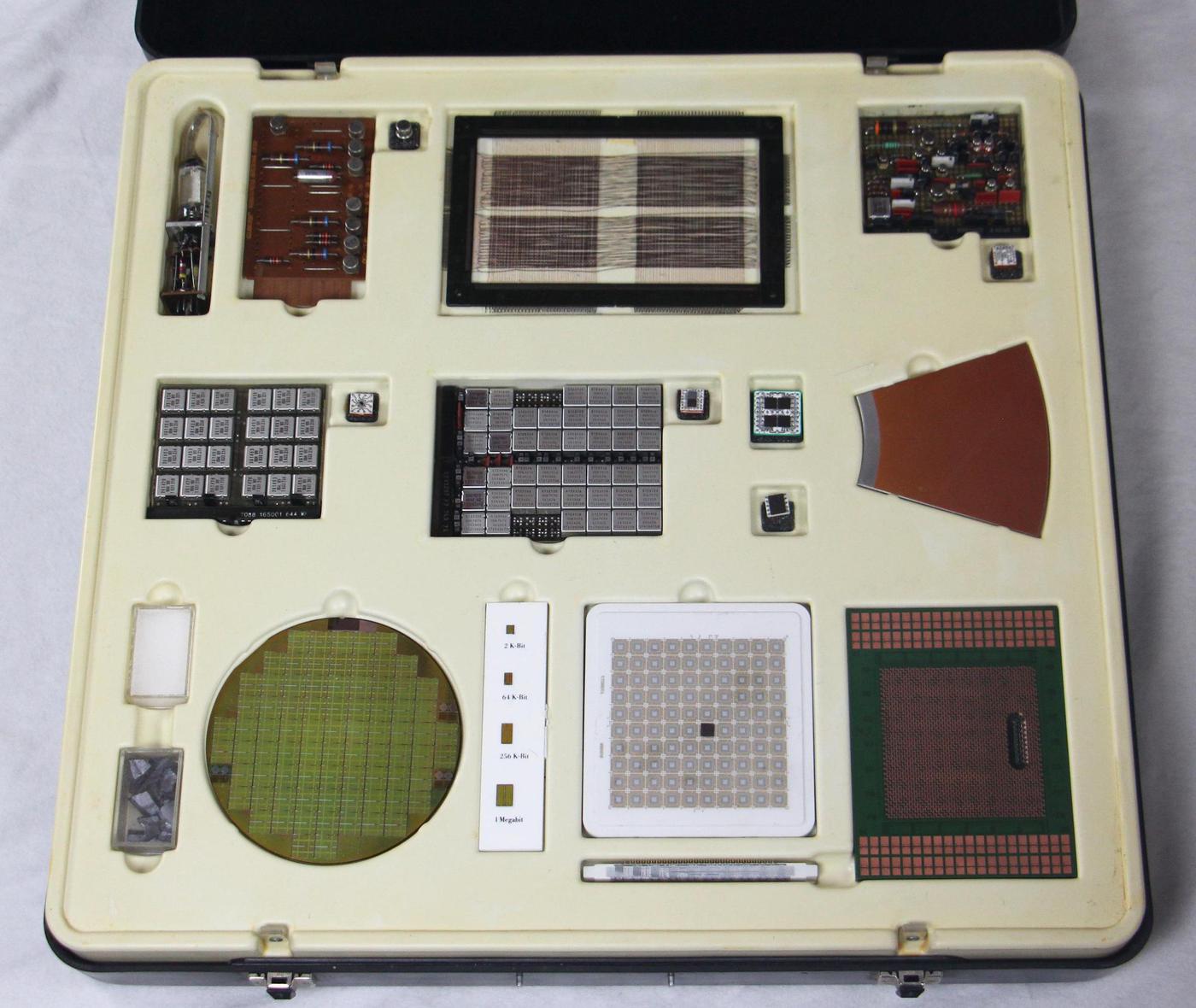
I recently received a vintage display box used by IBM to illustrate the progress of computer technology. This display case, created by IBM Germany1 in 1986 included technologies ranging from vacuum tubes and magnetic core memory to IBM's latest (at the time) memory chips and processor modules. In this blog post, I describe these items in detail and how they fit into IBM's history.

An IBM display box, showing components and board from different generations of computing. Click this (or any other photo) for a larger image.

An IBM display box, showing components and board from different generations of computing. Click this (or any other photo) for a larger image.

First-generation computing: tube module

IBM is older than you might expect. It was created through merger (under the name CTR) in 1911 and produced punched card equipment for data processing, among other things. By the 1930s, IBM was producing complex electromechanical accounting machines for data processing, controlled by plugboards and relays.

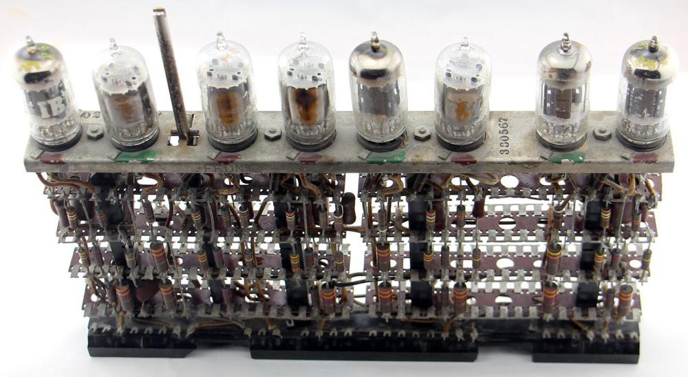
The so-called first generation of electronic computers started around 1946 with the use of vacuum tubes, which were orders of magnitude faster than electromechanical systems. Appropriately, the first artifact in the box is an IBM pluggable tube module. The pluggable module combined a vacuum tube along with its associated resistors and capacitors. These modules could be tested before being assembled into the system, and also replaced in the field by service engineers. Pluggable modules were also innovative because they packed the electronics efficiently into three-dimensional space, compared to mounting tubes on a flat chassis.

Tube module from an IBM 604 Electronic Calculating Punch.

Tube module from an IBM 604 Electronic Calculating Punch.

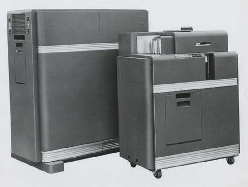
The pluggable tube module is from an IBM 604 Electronic Calculating Punch (1948). This large machine was not quite a computer, but it could add, subtract, multiply, and divide. It read 100 punch cards per minute, performed operations, and then punched the results onto new punch cards. It was programmed through a plugboard and could perform up to 60 operations per card. The IBM 604 was a popular product, with over 5600 produced. A typical application was payroll, where the 604 could compute various tax rates through multiplication.

The IBM 604 Electronic Calculating Punch behind a Type 521 Card Reader/Punch. Photo from IBM.

The IBM 604 Electronic Calculating Punch behind a Type 521 Card Reader/Punch. Photo from IBM.

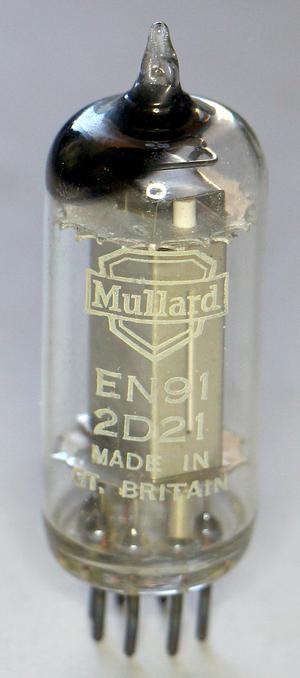
The 604 used many different types of tube modules. A typical module implemented an inverter, which could be used in an OR or AND gate.2 The tube module in the display box, however, is a thyratron driver, type MS-7A. The thyratron tube isn't exactly a vacuum tube since it is filled with xenon. This tube acts as a high-current switch; when activated, the xenon ionizes and passes the current. In the 604, thyratron tubes were used to drive relay coils or magnet coils in the card punch.3

A thyratron tube, type 2D21. This tube is from the pluggable module in the box.

A thyratron tube, type 2D21. This tube is from the pluggable module in the box.

Although the 604 wasn't quite a computer, IBM went on to build various vacuum-tube computers in the 1950s. These machines used larger pluggable tube modules that each held 8 tubes.4 The box didn't include one of these modules—probably due to their size—but I've included a photo below because of their historical importance.

A key-debouncing module from an IBM 705. Details here.

A key-debouncing module from an IBM 705. Details here.

Second generation: transistors and SMS (Standard Modular System) card

With the development of transistors in the 1950s, computers moved into the second generation, replacing vacuum tubes with smaller and more reliable transistors. IBM based its transistorized computers on pluggable cards called Standard Modular System (SMS) cards. These cards were the building block of IBM's transistorized computers including the compact IBM 1401 (1959), and the larger 7000-series mainframe systems. A computer used thousands of SMS cards, manufactured in large numbers by automated machines.

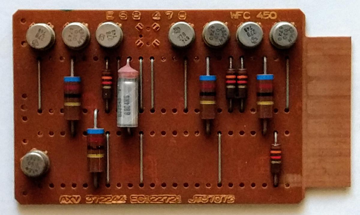
The photo below shows the SMS card from the box.5 The card is a printed circuit board, about the size of a playing card, with components and jumpers on one side and wiring on the back. A typical SMS card had a few transistors and implemented a simple function such as a gate. The cards used germanium transistors in metal cans as silicon transistors weren't yet popular. I've written about SMS cards before if you want more details.

The SMS card in the technology box, type AXV.

The SMS card in the technology box, type AXV.

Third generation: SLT (Solid Logic Technology)

In 1964, IBM introduced the System/360 line of mainframe computers. The revolutionary idea behind System/360 was to use a single architecture for the full circle (360°) of applications: from business to scientific computing, and from low-end to high-end systems. (Prior to System/360, different models of computers had completely different architectures and instruction sets, so each system required its own software.) The System/360 line was highly successful and cemented IBM's leadership in mainframe computers for many years.

Although other manufacturers used integrated circuits for their third generation computers, IBM used modules called SLT (Solid Logic Technology), which were not quite integrated circuits. Each thumbnail-sized SLT module contained a few discrete transistors, diodes, and resistors on a square ceramic substrate. An SLT module was capped with a square metal case, giving it a distinct appearance. Although an SLT module doesn't achieve the integration of an IC, it provides a density improvement over individual components. Each small SLT module was roughly equivalent to a complete SMS card, but much more reliable.7 By 1966, IBM was producing over 100 million SLT modules per year at a cost of 40 cents per module.6

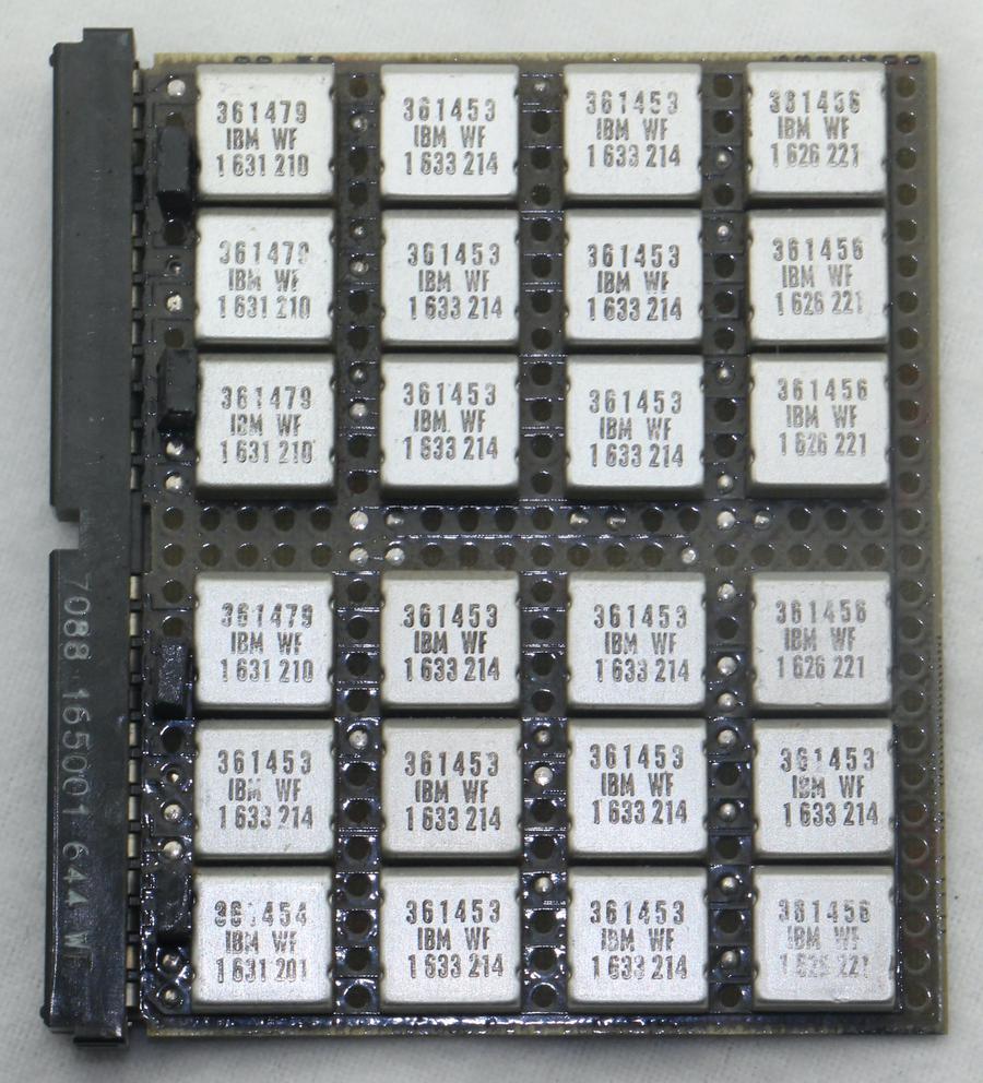
The board below is a logic board using 24 SLT modules. These modules implement AND-OR-INVERT logic gates, the primary logic circuit used in System/360. This board was probably part of the CPU.

A logic board using SLT modules. (The display box labeled this as an MST board though.)

A logic board using SLT modules. (The display box labeled this as an MST board though.)

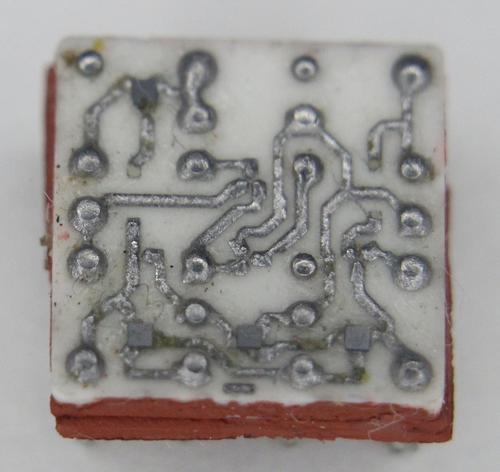
The photo below shows the circuitry inside an SLT module. This module has four transistors (the tiny gray squares). SLT modules typically include thick-film resistors, but none are visible in this module.

Closeup of an SLT module showing the tiny silicon dies mounted on the ceramic substrate.

Closeup of an SLT module showing the tiny silicon dies mounted on the ceramic substrate.

The box also has an SLT card with analog circuitry (maybe for the computer's core memory or power supply). This card has one SLT module, a simple module that contains four transistors (number 361457). I don't know why this board has so many discrete transistors; perhaps they are higher-power transistors than SLT modules provided.

A card using an SLT module (the metal square in the lower left).

A card using an SLT module (the metal square in the lower left).

Integrated circuits: MST (Monolithic System Technology)

For a few years, IBM used SLT modules while other computer manufacturers used integrated circuits. Eventually, though, IBM moved to integrated circuits, which they called Monolithic System Technology (MST). An MST module looks like an SLT module from the outside, but inside it contains a monolithic die (i.e. an integrated circuit) rather than the discrete components of SLT. MST was first used in 1969 for the low-end System/3 computer.

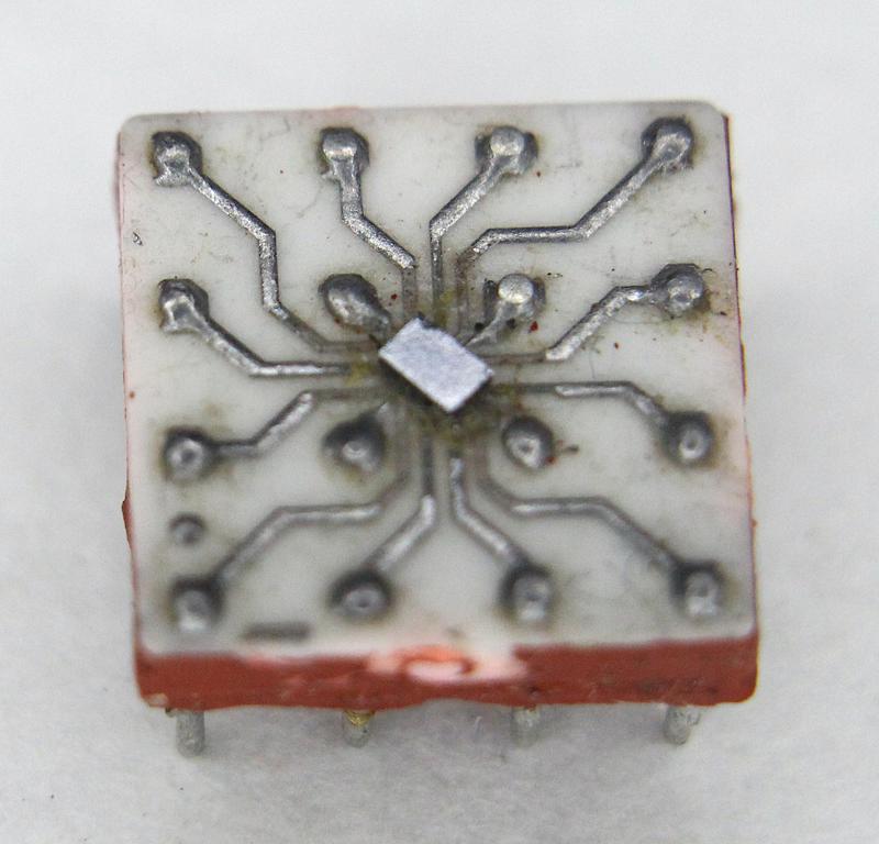
An MST module looks like an SLT module from the outside, but has an integrated circuit die inside.

An MST module looks like an SLT module from the outside, but has an integrated circuit die inside.

The photo above shows the box's MST module. The silicon die is the tiny shiny rectangle in the middle, connected to the 16 pins of the module. The chip was mounted upside down, soldered directly to the substrate. This upside-down mounting is unusual; most other manufacturers used ceramic or plastic packages for integrated circuits, with the silicon die connected to the pins via bond wires.

Core memory

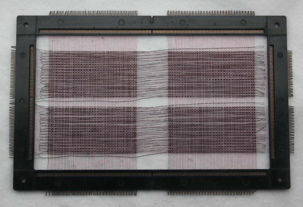
The box contains a core memory plane; most computers from the 1950s until the early 1970s used magnetic core memory for their main memory.8 This plane holds 8704 bits and is from a System/360 Model 20, the lowest-cost and most popular computer in the System/360 line.9

Core plane from a System/360 Model 20.

Core plane from a System/360 Model 20.

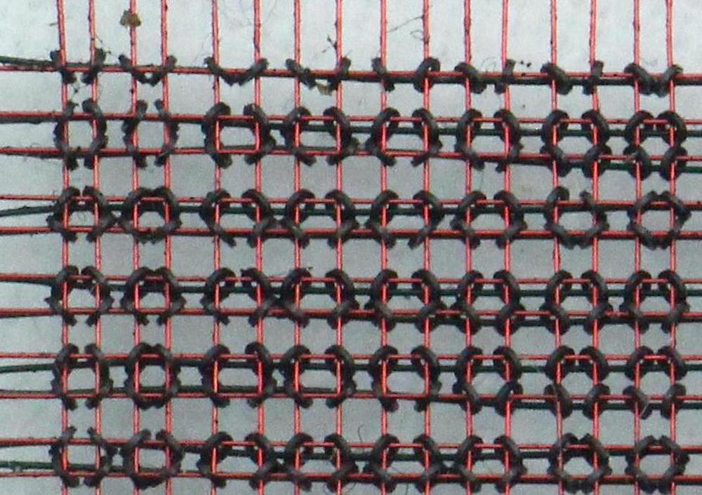
In core memory, each bit is stored in a tiny magnetized ferrite ring. The ferrite rings are organized into a matrix; by energizing a pair of wires, one bit is selected for reading or writing. Multiple core planes were stacked together to store words of data. Because each bit required a separate ferrite ring, magnetic core memory was limited in scalability. This opened the door for alternative storage approaches.

Closeup of the core plane, showing the wires through the tiny ferrite cores.

Closeup of the core plane, showing the wires through the tiny ferrite cores.

Semiconductor memory

IBM was an innovator in semiconductor memory and this is reflected in the numerous artifacts in the box that show off memory technology.10 Modern computers use a type of memory chip called DRAM (dynamic RAM), storing each bit in a tiny capacitor. DRAM was invented at IBM in 1966 and IBM continued to make important innovations in semiconductor memory.

Although magnetic core memory was the dominant RAM storage technique in the 1960s, IBM decided in 1968 to focus on semiconductor memory instead of magnetic core. The first computer to use semiconductor chips for its main memory12 was the IBM System/370 Model 145 mainframe (1970). Each chip in that computer held just 128 bits, so a computer might need tens of thousands of these chips.11 Fortunately, memory density rapidly increased, as shown by the dies below. I'll discuss the 2-kilobit chip in detail; my die photos of the others are in the footnotes13.

The box includes a display with four memory dies: 2 K-Bit, 64 K-Bit, 256 K-Bit, 1 Megabit.

The box includes a display with four memory dies: 2 K-Bit, 64 K-Bit, 256 K-Bit, 1 Megabit.

The photo below shows the 2-kilobit die14 under a microscope. It is a static RAM chip from 1973, not as dense as DRAM since it uses six transistors per bit. The tiny white lines on the chip are the metal layer on top of the silicon, wiring the circuitry together. Around the outside of the die are 26 solder bumps for attaching the chip to the substrate. Note that this chip is mounted upside down ("flip-chip") on the substrate, unlike most integrated circuits that use bond wires. The chip is covered with a protective yellowish film, except where the solder bumps are located.

Die photo of the 2-kilobit chip.

Die photo of the 2-kilobit chip.

To increase the density of storage, four of these chips were mounted in a two-layer MST module, yielding an 8-kilobit module. The module in the box (below) has the square metal case removed, showing the silicon dies inside. These memory modules provided the main memory for the IBM System/370 models 115 and 125, as well as the memory expansion for the models 158 and 168 (1972).

The memory module has chips on two levels. This is an 8-kilobit module composed of four 2-kilobit chips.

The memory module has chips on two levels. This is an 8-kilobit module composed of four 2-kilobit chips.

Each memory card (below) contained 32 of these modules to provide 32 kilobytes of storage. In the photo below, you can see the double-height memory modules along with shorter modules for support circuitry. A four-megabyte main memory unit held 144 of these cards in a frame about 3 feet × 3 feet × 1 foot, so semiconductor memory was still fairly bulky in 1972.

The memory board contains regular MST modules and double-height modules that hold the memory chips.

The memory board contains regular MST modules and double-height modules that hold the memory chips.

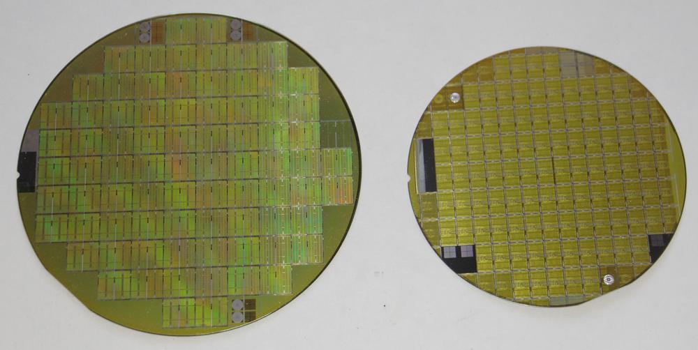
Moving along to some different memory chips, the box includes two silicon wafers holding memory dies, a 5" wafer and a 4" wafer.

The two silicon wafers.

The two silicon wafers.

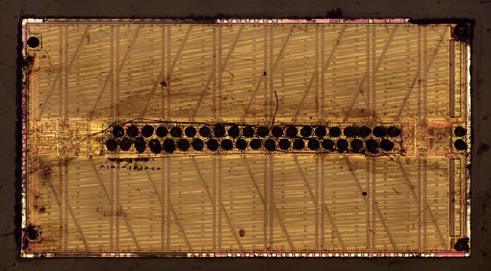
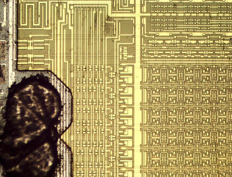
The smaller four-inch wafer (1982) holds 288-kilobit dynamic RAM chips, an unusual size as it isn't a power of 2.15 The explanation is that the chip holds 32 kilobytes of 9-bit bytes (8 + parity). In the die photo, you can see that the memory array is mostly obscured by complex wiring on top of the die. This wiring is due to another unusual part of the chip's design: for the most efficient layout, the memory bit lines have a different spacing from the bit decode lines. As a result, irregular wiring is required to connect the parts of the chip together, forming the pattern visible on top of the chip. Because this die is on the wafer, you can see the alignment marks and test circuitry around the outside of the chip.

Die photo of the 4" wafer.

Die photo of the 4" wafer.

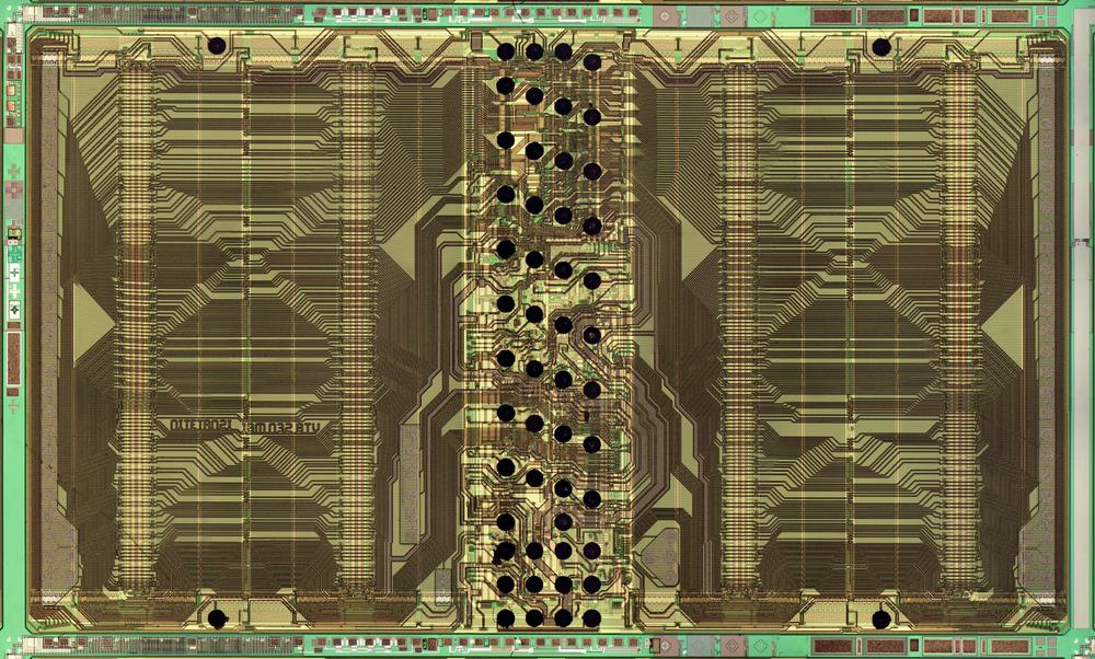
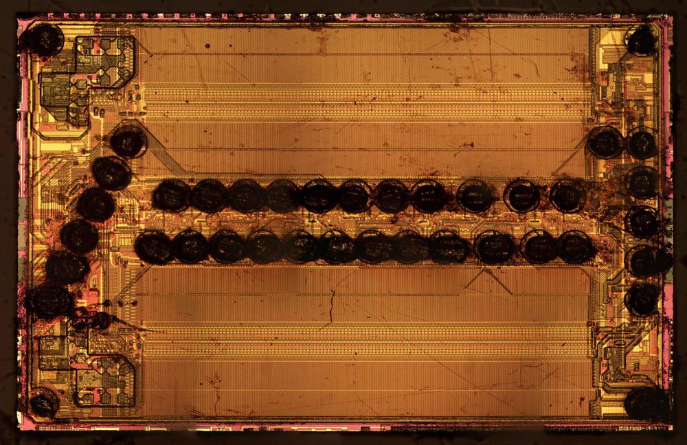
The five-inch wafer holds 1-megabit memory chips16 that were used in the IBM 3090 mainframe17 (1985). This computer used circuit cards with 32 of these chips, providing four megabytes of storage per card, a huge improvement over the 32-kilobyte card described earlier. The 3090 used multiple memory cards, providing up to 256 megabytes of main storage. The die photo below shows how the chip consists of 16 rectangular subarrays, each holding 64 kilobits.

Die photo of the 1-megabit DRAM chip on the 5" wafer. The dark circles are dirt, not solder balls.

Die photo of the 1-megabit DRAM chip on the 5" wafer. The dark circles are dirt, not solder balls.

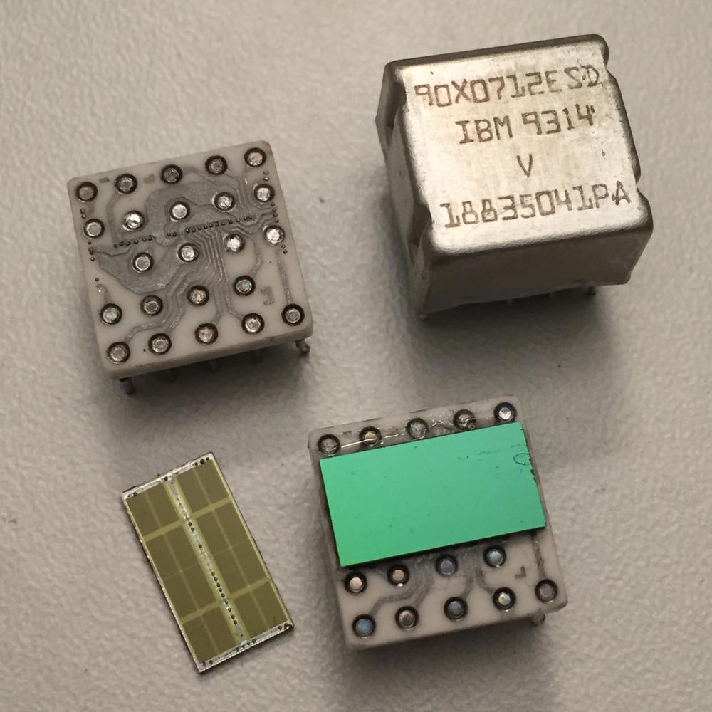
The photo below shows how this die is mounted upside-down on the ceramic substrate with the solder bumps connected to the 23 pins of the module. This module (not part of the box) was used in the IBM PS/2 personal computer.18 The die below looks green, unlike the die above, but that's just due to the lighting.

Construction of an IBM memory module. This module was not part of the box, but the die is the same as the 5" die. Photo courtesy of Antoine Bercovici.

Construction of an IBM memory module. This module was not part of the box, but the die is the same as the 5" die. Photo courtesy of Antoine Bercovici.

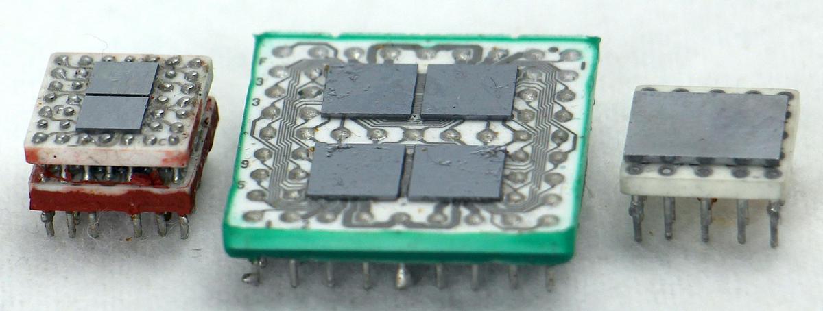
The photo below compares three memory modules from the technology box. The first module is the 8-kilobit module containing four 2-kilobit chips, described earlier. The second module is a much wider 512-kilobit module, built from four 128-kilobit dies. The third module contains a 1-megabit chip (the one in the 4-chip display, not from the wafer). These megabit modules were used in the IBM 3090 mainframe's secondary storage.

Three memory modules: 8-kilobit, 512-kilobit, and 1-megabit.

Three memory modules: 8-kilobit, 512-kilobit, and 1-megabit.

Disk platter

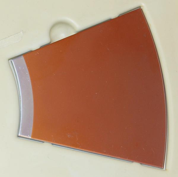
The box contains a segment of a 14" IBM disk platter, used in disk storage systems from minicomputers to mainframes. IBM was a pioneer in hard disks, starting with the IBM RAMAC (1956), which weighed over a ton and held 5 million characters on a stack of 24" platters. IBM switched to 14" platters in 1961 and by 1980 the IBM 3380 disk system held up to 2.5 gigabytes in a large cabinet of 14" platters.19 The 14" platter was also popular in low-cost, removable disk cartridge (1965) used with many minicomputers. The 14" disk platter was finally replaced by an 11" platter with the introduction of the IBM 3390 disk drive in 1989. Nowadays, laptops typically use 2.5" platters; amazingly, disk capacity kept increasing as disk diameter steeply decreased.

Section of a 14" disk platter from the display box.

Section of a 14" disk platter from the display box.

Artifacts from the IBM 3090

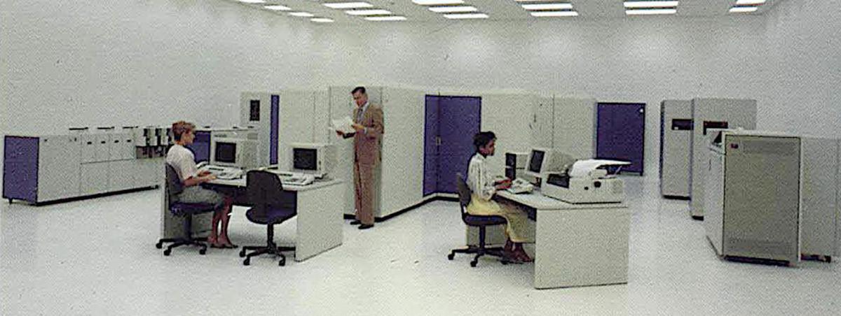
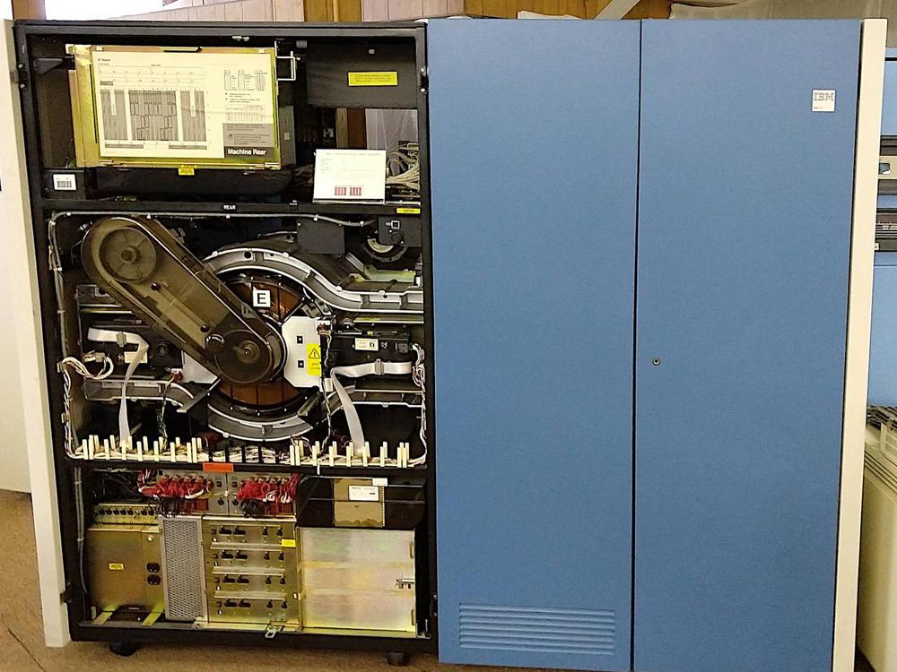
At the time of the box's creation, the 3090 mainframe was IBM's new high-performance computer (below), so the box has several artifacts that show off the technology in this computer. Although the IBM 3090 (1985) had top-of-the-line performance at the time, by 1998 an Intel Pentium II Xeon microprocessor had comparable performance,20 illustrating the remarkable improvements of microprocessor technology.

An IBM 3090 data center. Photo from the IBM 3090 brochure.

An IBM 3090 data center. Photo from the IBM 3090 brochure.

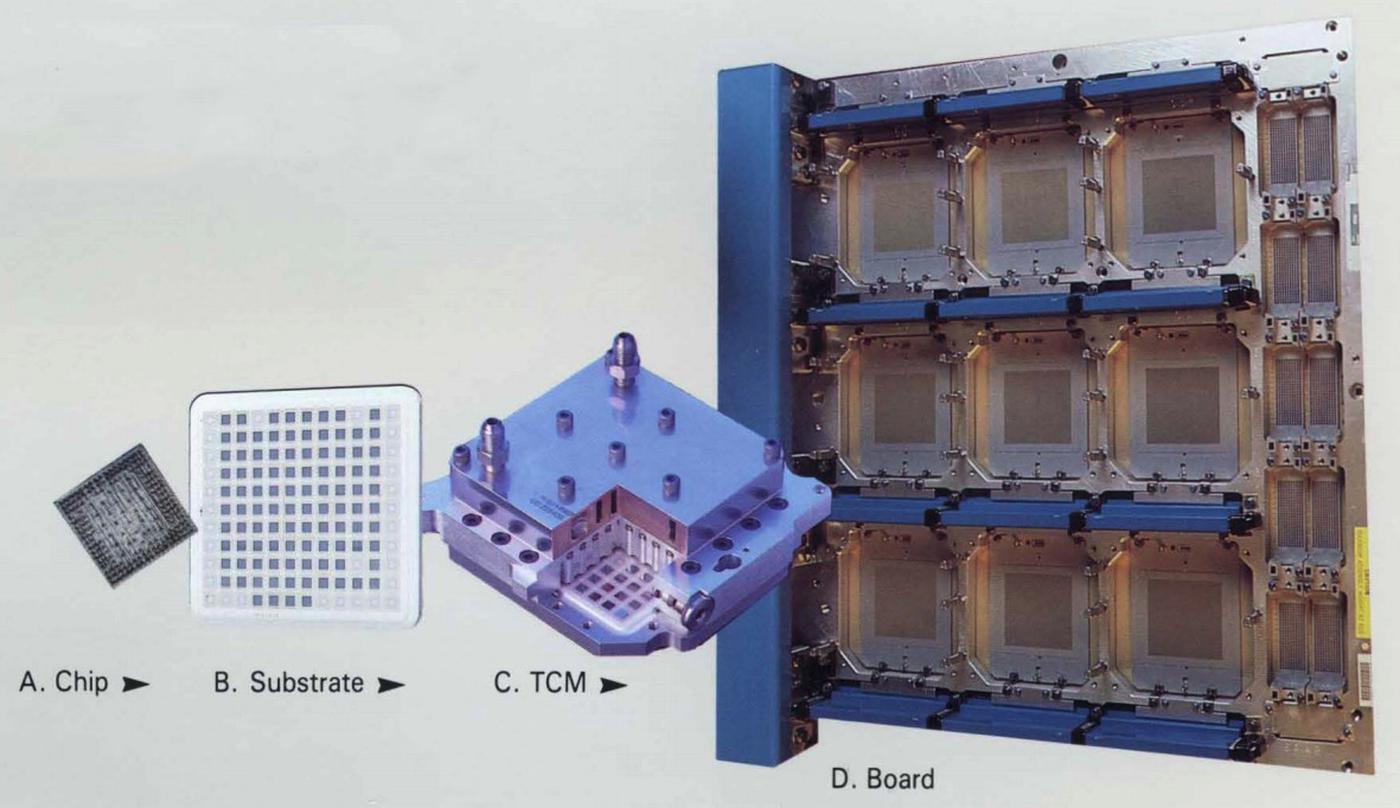
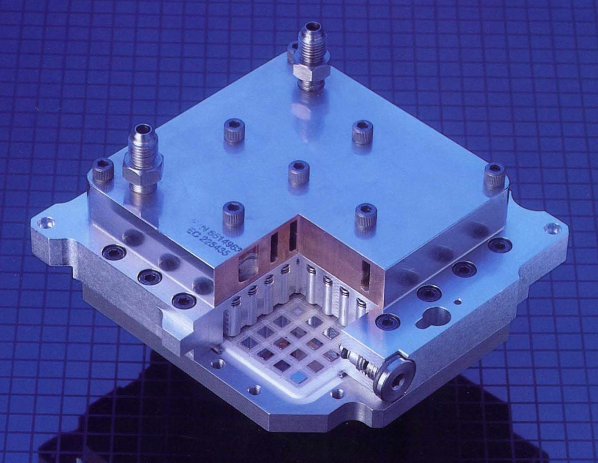
In 1980, IBM introduced the thermal conduction module (TCM), an advanced way to package integrated circuits at high density, while removing the heat that they generate.21 A TCM starts with a multi-chip module with about 100 high-speed integrated circuits mounted on a ceramic substrate, as shown below. This substrate contains dozens of wiring layers to connect the integrated circuits.22 To remove the heat, the ceramic substrate is packaged in a TCM, which has a metal piston contacting each silicon die. These pistons are surrounded by helium (which conducts heat better than air), and the whole TCM package is water-cooled. Finally, nine TCMs are mounted on a printed circuit board.

The hierarchy of components in the IBM 3090: chips are mounted on a ceramic substrate, which is assembled into a TCM. A board holds nine TCMs.

The hierarchy of components in the IBM 3090: chips are mounted on a ceramic substrate, which is assembled into a TCM. A board holds nine TCMs.

This incredibly complex heat-removal system was required because the 3090 used emitter-coupled logic (ECL), the same type of circuitry used in the Cray-1 supercomputer. Although ECL is a very fast logic family, it is also power-hungry and generates much more heat than the MOS transistors used in microprocessors.

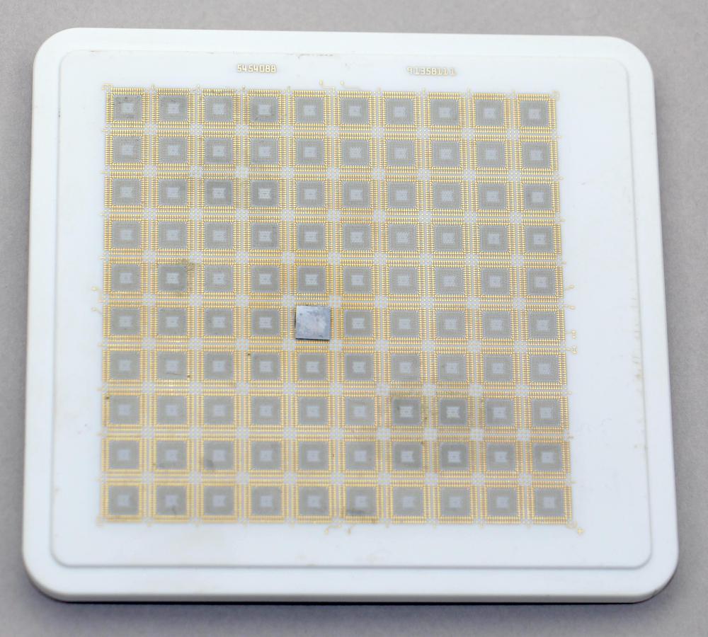
The ceramic substrate for a TCM, from the box. It is fairly small, measuring 11&times11.7 cm. This substrate holds 100 silicon dies; one is visible near the middle.

The ceramic substrate for a TCM, from the box. It is fairly small, measuring 11×11.7 cm. This substrate holds 100 silicon dies; one is visible near the middle.

The photo above shows the ceramic substrate. Normally, the substrate has 100 silicon dies mounted on it, but this sample has just a single die. The box also includes a cross-section slice of the ceramic substrate (below). This shows the 38 layers of wiring inside the substrate, as well as the pins on the underside.

Cross-section of the ceramic substrate, showing the multiple layers of internal wiring.

Cross-section of the ceramic substrate, showing the multiple layers of internal wiring.

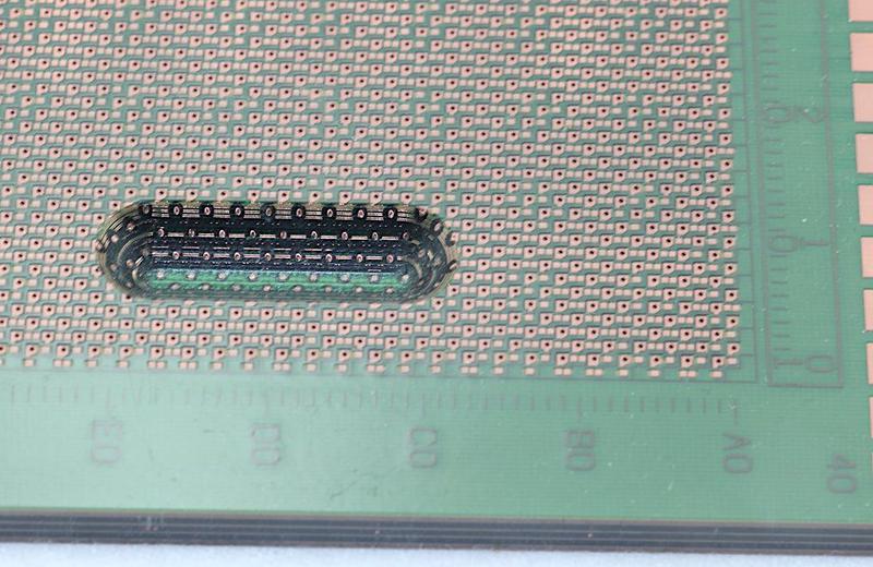
Each TCM had 1800 pins so it could be plugged into a printed circuit board and connected to the rest of the system. Each board held 9 TCMs and was powered with an incredible 1400 amps. The box includes a PCB sample, showing its multi-layer construction (below), and the dense grid of holes to receive the ceramic substrate.

Closeup of the printed circuit board used in the IBM 3090. The routed groove shows the multi-layer construction.

Closeup of the printed circuit board used in the IBM 3090. The routed groove shows the multi-layer construction.

Finally, here's a nice cutaway of a TCM from the detailed IBM 3090 brochure. At the bottom, it shows the silicon dies mounted on the ceramic substrate. The dies are contacted by the heat sink pistons in the middle. The connections on top are for the cooling water.

This cut-away image from IBM shows the internal construction of a TCM.

This cut-away image from IBM shows the internal construction of a TCM.

Conclusion

This technology exhibit box was created 35 years ago. Looking at it from the present provides a perspective on the history of both IBM and the computer industry. The box's date, 1986, marks the peak of IBM's success and influence,23 right before microcomputers decimated the mainframe market and IBM's dominance. What I find interesting is that the technology box focuses on mainframes and lacks any artifacts from the IBM PC (1981), which ended up having much more long-term impact..24 This neglect of microcomputers reflects IBM's corporate focus on the mainframe market rather than the PC market (which, ironically, IBM created).

In the bigger historical picture, the technology box covers a time of great upheaval as electromechanical accounting machines were replaced by three generations of computers in rapid succession: vacuums tubes, then transistors, and finally integrated circuits. In contrast to this period of rapid change, nothing has replaced integrated circuits over the past 50 years. Instead, integrated circuits have remained, but improved by many orders of magnitude, as described by Moore's Law. (Compared to the room-filling IBM 3090 mainframe, an iPhone has 1000 times the performance and 50 times the RAM.) Will integrated circuits continue their dominance for the next 50 years or will some new technology replace them? It remains to be seen.

Thanks to Cyprien for providing this amazing box of artifacts. I announce my latest blog posts on Twitter, so follow me @kenshirriff. I also have an RSS feed.

Notes and references

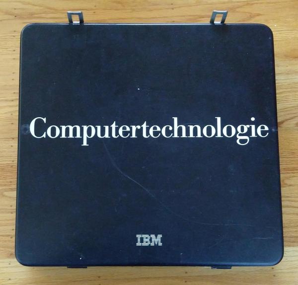
  1. The box was apparently created in Stuttgart, Germany. The components are protected by a piece of plexiglass, with labels in German for all the components, such as Mehrschicht-Keramiktrager for multi-layer ceramic substrate. The labels are listed here if you're interested.

    The box is labeled in German: "Computertechnologie".

    The box is labeled in German: "Computertechnologie".

    The box originally included several German books on computer technology but since they are missing I had to do some research and come up with my own narrative.


  2. For more information on the pluggable tube modules, see the schematics of IBM's pluggable units (which lack the box's MS-7A module). (I suspect the MS-7A was selected for the box because it is more compact than most of the pluggable modules, having one layer of circuitry below the tube, rather than two.) 

  3. The IBM 604 service manual says that the thyratron tube modules are designated TH, but the module in the box is designated MS-7A. I don't know why the designations don't match up. 

  4. People sometimes think that an 8-tube module held a byte. This is wrong for two reasons. First, bytes didn't exist back then. IBM's early scientific computers used 36-bit words, while the business computers were based on characters of 6 bits plus parity. Second, 8 tubes didn't correspond to 8 bits because circuits often required multiple tubes. For instance, a tube module could implement three bits of register storage. 

  5. The SMS card in the box is type AXV, a complementary emitter follower circuit used in the IBM 1443 printer and other systems. 

  6. SLT was controversial, since other companies used more-advanced integrated circuits rather than hybrid modules. In typical IBM fashion, the vice president in charge of SLT was demoted in 1964, only to be reinstated in 1966 when SLT proved successful. My view is that integrated circuit technology was too immature when the System/360 was released, so IBM's choice to use SLT made the System/360 possible. However, it only took a year before integrated circuits became practical, as shown by their use in competing mainframes. I think IBM stuck with SLT modules longer than necessary. Integrated circuits rapidly increased in complexity (Moore's Law), while SLT modules could only increase density through hacks such as putting resistors on the underside (SLD) and using two layers of ceramic (ASLT). 

  7. Curiously, this card is labeled in the box as an MST card, but checking the part numbers shows it has SLT modules. Specifically, it contains the following types of SLT modules (click for details): 361453 AND-OR-Invert, 361454 inverters, 361456 AND-OR-extender, and 361479 inverters. The SLT modules are also documented in IBM's manual.

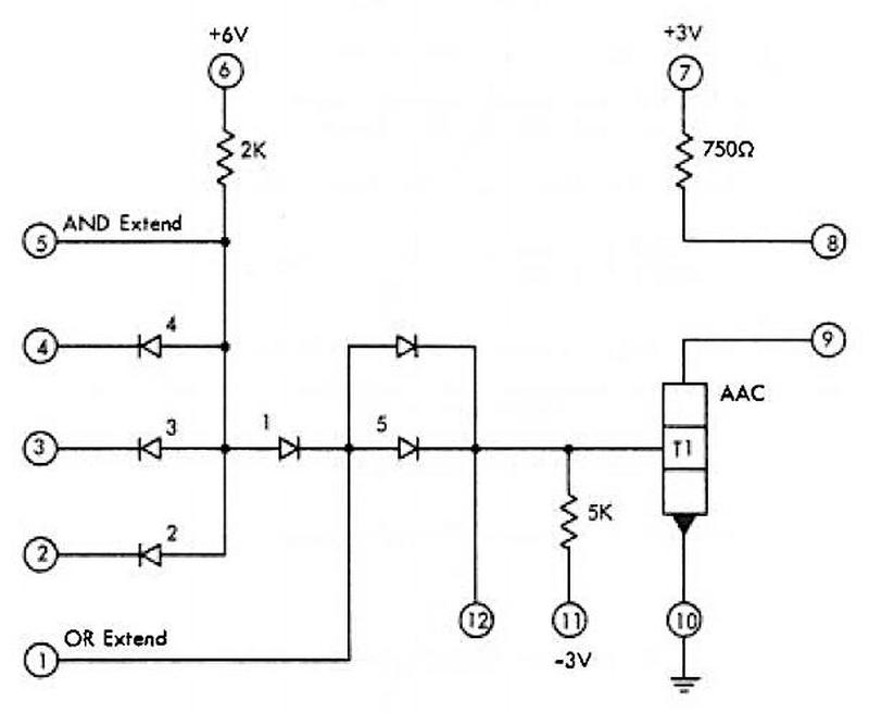
    Schematic of one of the SLT modules on the board (361453 AND-OR-INVERT (AOI) gate) from the IBM manual.

    Schematic of one of the SLT modules on the board (361453 AND-OR-INVERT (AOI) gate) from the IBM manual.

    The schematic above shows one of the SLT modules. (IBM had their own symbol for transistors; T1 is an NPN transistor.) This gate is built from diode-transistor-logic, so it's more primitive than the TTL logic that became popular in the late 1960s. The "Extend" pins are used to connect modules together to build larger gates, so the modules provide a lot of flexibility. This module inconveniently requires three voltages. This SLT module contained one transistor die, three dual-diode dies, and three thick-film resistors. During manufacturing, the resistors were sand-blasted to obtain accurate resistances, an advantage over the inaccurate resistances on integrated circuit dies. 

  8. The System/360 line was designed as a single 32-bit architecture for all the models. The Model 20, however, is a stripped-down, 16-bit version of System/360, incompatible with the other machines. (Some people don't consider the Model 20 a "real" System/360 for this reason.) But due to its low price, the Model 20 was the most popular System/360 with more than 7,400 in operation by the end of 1970. 

  9. This core memory plane from a System/360 Model 20 is a 128×68 grid. Note that this isn't a power of 2: the plane provided 8192 bits of main memory storage as well as 512 bits for registers. Using the same core plane for memory and registers hurt performance but saved money. The computer used five of these planes to make a 4-kilobyte memory module, or 10 planes for an 8-kilobyte module. For details, see the Model 20 Field Engineering manual

  10. For an extensive list of references on DRAM chips, see the thesis Impact of processing technology on DRAM sense amplifier design (1990). For a history of memory development at IBM through 1980, from ferrite core to DRAM, see Solid state memory development in IBM

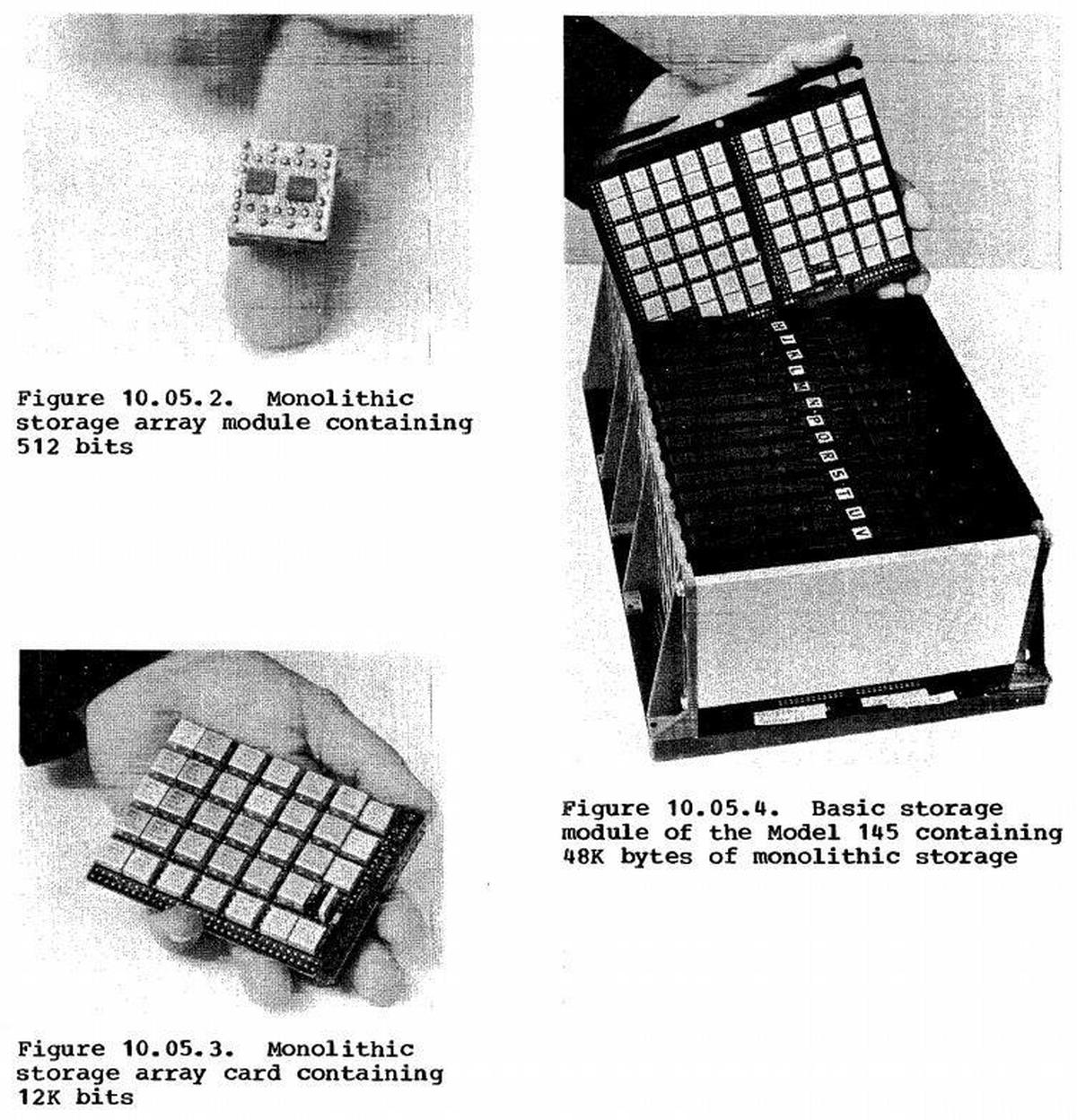
  11. The System/370 Model 145 was the first computer with semiconductor main memory. Each thumbnail-sized MST module held four 128-bit chips; 24 modules fit onto a 12-kilobit storage card. A shoebox-sized Basic Storage Module held 36 cards, providing 48 kilobytes of storage with parity. By modern standards this storage is incredibly bulky, but it provided twice the density of the magnetic core memory used by contemporary systems. The computer's storage consisted of up to 16 of these boxes in a large cabinet (or two), providing 112 kilobytes to 512 kilobytes of RAM.

    Photos showing the 512-bit memory module, the 12-kilobit memory card, and the 48-kilobyte basic storage module. Photos from IBM 370 guide.

    Photos showing the 512-bit memory module, the 12-kilobit memory card, and the 48-kilobyte basic storage module. Photos from IBM 370 guide.


  12. IBM had used monolithic memory for special purposes earlier, holding the "storage protect" data in the IBM 360/91 (1966) and providing a memory cache in the System/360 Model 85.  

  13. I wasn't able to find exact details on the 64-kilobit, 256-kilobit, and 1-megabit chips from the display, but I took die photos.

    Die photo of the 64k memory chip.

    Die photo of the 64k memory chip.

    The 64-kilobit chip is shown above. The solder balls are the most visible part of the chip. The article A 64K FET Dynamic Random Access Memory: Design Considerations and Description (1980) describes IBM's experimental 64-kilobit DRAM chip, but the chip they describe doesn't entirely match the chip in the box. There were probably some significant design changes between the prototype chip and the production chip.

    Die photo of the 256-kilobit RAM, roughly 1985.

    Die photo of the 256-kilobit RAM, roughly 1985.

    The 256-kilobit die is shown above. The diagonal lines on the die are similar, but not identical, to the die in A 256K NMOS DRAM (1984). That chip was designed at IBM Laboratories in Böblingen, Germany, and could provide 1, 2, or 4 bits in parallel.

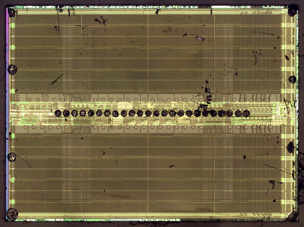
    Die photo of the 1-megabit memory chip.

    Die photo of the 1-megabit memory chip.

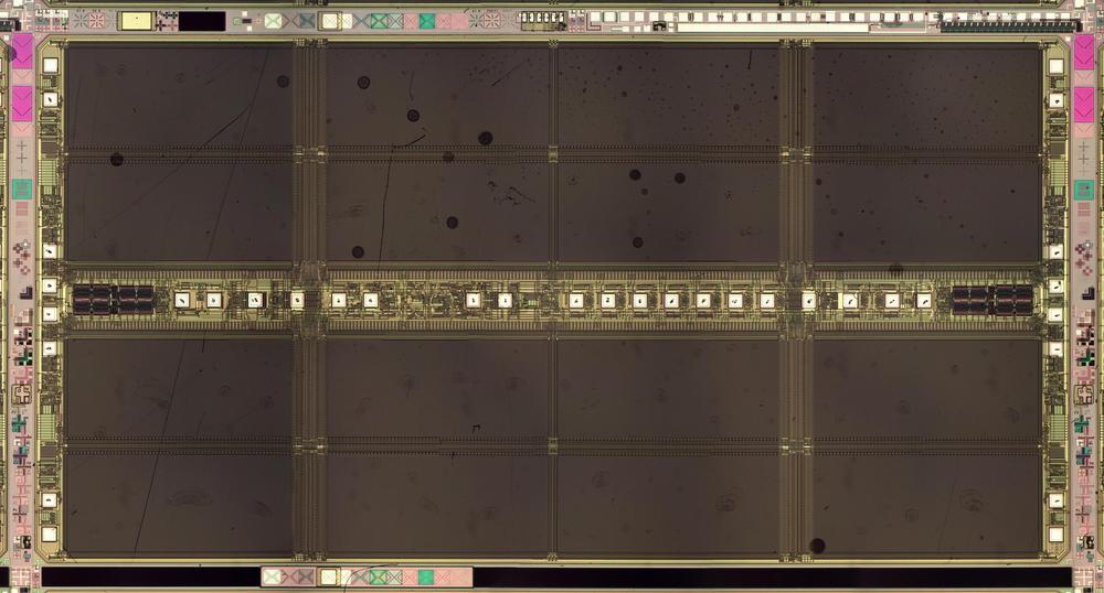
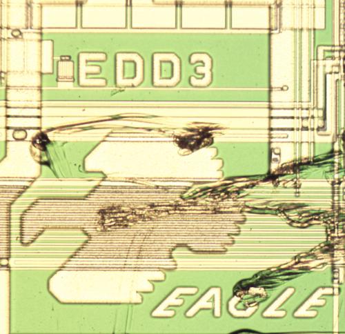
    The 1-megabit die is shown above. IBM was the first company to begin volume production of 1-megabit memory chips and the first company to use them in mainframe computers. This chip was used in the IBM 3090 mainframe, but was later replaced by the faster and smaller "second-generation" 1-megabit chip on the 5" wafer. One interesting feature of this die is the "eagle" logo, shown below.

    The eagle chip art on the 1-megabit RAM chip, slightly scratched.

    The eagle chip art on the 1-megabit RAM chip, slightly scratched.

    The box includes a 1-megabit MST module (below) that uses this chip. Because the chip's solder balls are along its center, the module omits the center three pins to make room for the connections to the chip.

    The 1-megabit chip mounted in an MST module.

    The 1-megabit chip mounted in an MST module.


  14. This memory card and its 2-kilobit chips are described in detail in A High Performance Low Power 2048-Bit Memory Chip in MOSFET Technology and Its Application (1976). These modules were used in the main memory of the IBM System 370 models 115 (1973) and 125 (1972) as well as upgraded memory for the models 158 (1972) and 168 (1972). The IBM System/360 Model 138 (1976) and Model 148 (1976) also used 2K MOSFET chips, presumably the same ones. The 2-kilobit chip was developed at IBM Laboratories in Böblingen, Germany; this may have motivated its inclusion in this German display box. The chip was codenamed Riesling and IBM made millions of them.

    Closeup of the 2-kilobit RAM chip.

    Closeup of the 2-kilobit RAM chip.

    The closeup of the 2-kilobit die shows some of the decoder circuitry (left) and the storage cells (right). Two solder balls are in the lower left; the rest of the die is covered with a protective yellow film, probably polyimide. Each storage cell consists of six transistors. The chip is built with metal-gate NMOS transistors. 

  15. The 288-kilobit chip is described in detail in A 288Kb Dynamic RAM.

    Closeup of the IBM 288-kilobit memory chip showing the programmable fuses.

    Closeup of the IBM 288-kilobit memory chip showing the programmable fuses.

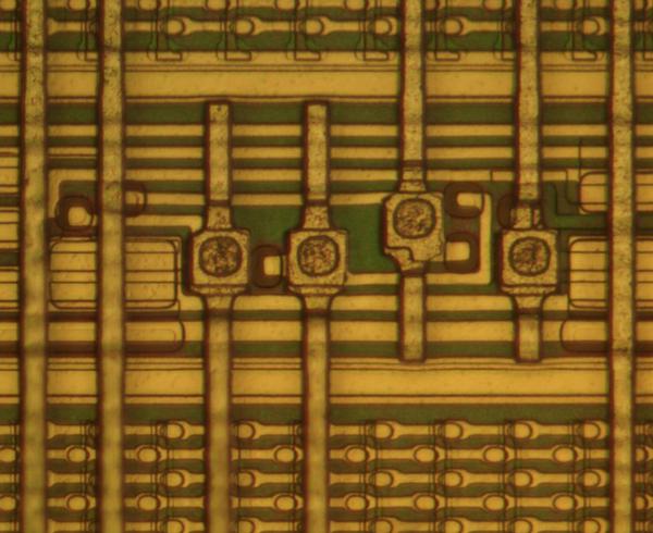
    The closeup die photo above shows some of the memory cells (at the top and bottom), wired into bit lines. One unusual feature of this chip is that has redundancy to work around faults. In particular, four redundant word lines can be substituted for faulty ones, by blowing configuration fuses. I think the large boxes with circles in the middle are four of the fuses.

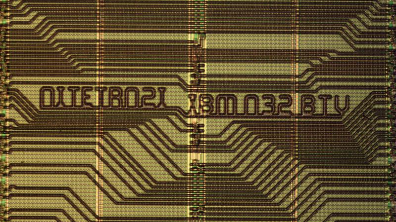
    The part number on the 4" die: OITETR02I IBM 032 BTV.

    The part number on the 4" die: OITETR02I IBM 032 BTV.

    The photo above shows the chip's part number; BTV refers to IBM's Burlington / Essex Junction, VT semiconductor plant where the chip was designed. This plant was acquired by GlobalFoundaries in 2015. This photo also shows the complex geometrical wiring, unlike the regular matrix in most memory chips. 

  16. Note that there are two 1-megabit chips in the box. The chip on the 4-chip display is an older chip than the one on the 5" wafer. The 1-megabit memory chip on the wafer is described in An Experimental 80-ns l-Mbit DRAM with Fast Page Operation (1985). It uses a single 5-volt power supply. The chip is structured as four 256-kbit quadrants, each subdivided into four 64-kbit subarrays. It has two redundant bit lines per quadrant for higher yield. The horizontal solder balls through the middle of the chip are the common connections for each quadrant, while the vertical connections along the left and right edges provide the signals specific to each quadrant. This quadrant structure allows the chip to be accessed as 256K×4 or 1M×1. 

  17. IBM's overview of the 3090 family provides details on the hardware, including the memory and TCM modules. Page 10 discusses IBM's memory technology as of 1987 and has a picture of their "second generation" 1-megabit chip, which matches the die on the 5" wafer. 

  18. The 1-megabit memory chips were used in the IBM 3090 mainframe, but I think the faulty ones were used in IBM PS/2 personal computer. You can see the unusual metal MST packages on many PS/2 cards. Specifically, if one of the four quadrants in the memory chip had a fault, the memory chip was used as a 3/4-megabyte chip. These had four part numbers, depending on the faulty quadrant: 90X0710ESD through 90X0713ESD (ESD probably stands for Electrostatic Sensitive Device). The PS/2 2-megabyte memory card (90X7391) had 24 chips providing 2 megabytes with parity. The board used chips with alternating bad banks so the memory regions fit together. 

  19. Since several of the artifacts in the box came from the IBM 3090 mainframe, and the 3380 disk system was used with the 3090 mainframe, my suspicion is that the platter is from the 3380 disk system, shown below.

    An IBM 3380E disk storage system, holding 5 gigabytes. The disk platters are center-left, labeled "E". Photo taken at the Large Scale Systems Museum.

    An IBM 3380E disk storage system, holding 5 gigabytes. The disk platters are center-left, labeled "E". Photo taken at the Large Scale Systems Museum.


  20. It's difficult to precisely compare different computers, especially since the 3090 supported multiple processors and vector units. I looked at benchmarks from 2001 comparing various computers on a linear algebra benchmark. The IBM 3090 performed at 97 to 540 megaflops/second for configurations of 1 to 6 processors respectively. An Intel Pentium II Xeon performed at 295 megaflops/second, a bit faster than the 3-processor IBM 3090. To compare clock speeds, the IBM 3090 ran at 69 MHz, while the Pentium ran at 450 MHz. An IBM 3090 cost $4 million while a Pentium II system was $7,000 to $20,000. The IBM 3090 came with 64 to 128 megabytes of RAM while people complained about the Pentium II's initial 512-megabyte limit. The point of this is that while the IBM 3090 was a powerful mainframe in 1985, microprocessors caught up in about 13 years, thanks to Moore's Law. 

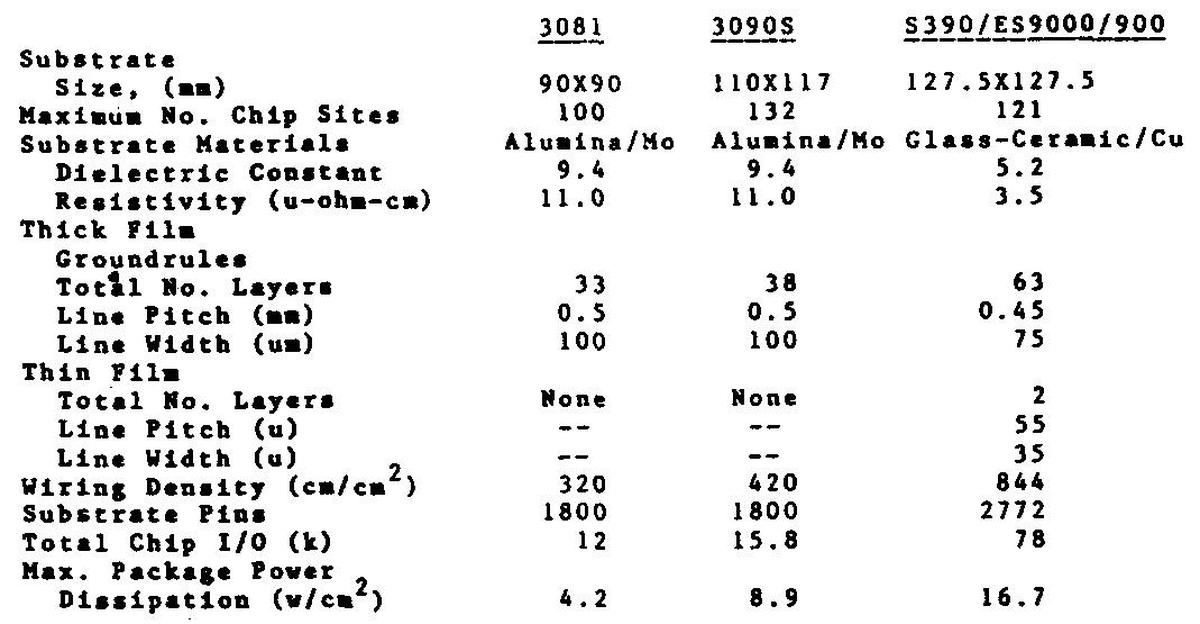
  21. The table below compares characteristics of the Thermal Conduction Modules used in the IBM 3081 (1980), IBM 3090 (1985), and IBM S/390 (1990) computers. The board-level technology progressed similarly. For instance, a 3081 board took up to 500 amps, while a 3090 board took 1400 amps, and an S/390 board took 3400 amps.

    This table of information on TCMs is from Packaging Technology for IBM's Latest Mainframe Computers (S/390/ES9000).

    The IBM 4300-series processors (1979) used a ceramic multi-chip module that held 36 chips, but it used an aluminum heat sink and air cooling instead of the more complex water-cooled TCM. The IBM 4381's smaller multi-chip module is often erroneously called a TCM by online articles, but it's a multilayer ceramic multichip module (MLC MCM). For more information about IBM's chip packaging, see this detailed web page

  22. For more information on TCMs, see the EEVblog teardown

  23. Desktop computer sales first exceeded mainframe computer sales in 1984. Counting the number of employees, IBM peaked in 1985 and declined until 1994 (source). 1985 was also a peak year for IBM's revenue and profits, according to The Decline and Rise of IBM. By 1991, IBM's problems were discussed by the New York Times. After heavy losses, IBM regained profitability and growth in the 1990s, but never regained its dominance of the computer industry. 

  24. Perhaps one reason that the technology box ignores IBM's personal computers is that these computers didn't contain IBM-specific hardware that they could show off: Intel built the 80x86 processor, while companies such as Texas Instruments built the memory and support integrated circuits. The lack of IBM-specific technology in these personal computers is one factor that led to IBM losing control of the PC-compatible market.