A circuit called the flip-flop is a fundamental building block for sequential logic. A flip-flop can hold one bit of state, a "0" or a "1", changing its value when the clock changes. Flip-flops are a key part of processors, with multiple roles. Several flip-flops can be combined to form a register, holding a value. Flip-flops are also used to build "state machines", circuits that move from step to step in a controlled sequence. A flip-flops can also delay a signal, holding it from from one clock cycle to the next.
Intel introduced the groundbreaking 8086 microprocessor in 1978, starting the x86 architecture that is widely used today. In this blog post, I take a close look at the flip-flops in the 8086: what they do and how they are implemented. In particular, I will focus on the dynamic flip-flop, which holds its value using capacitance, much like DRAM.2 Many of these flip-flops use a somewhat unusual "enable" input, which allows the flip-flop to hold its value for multiple clock cycles.
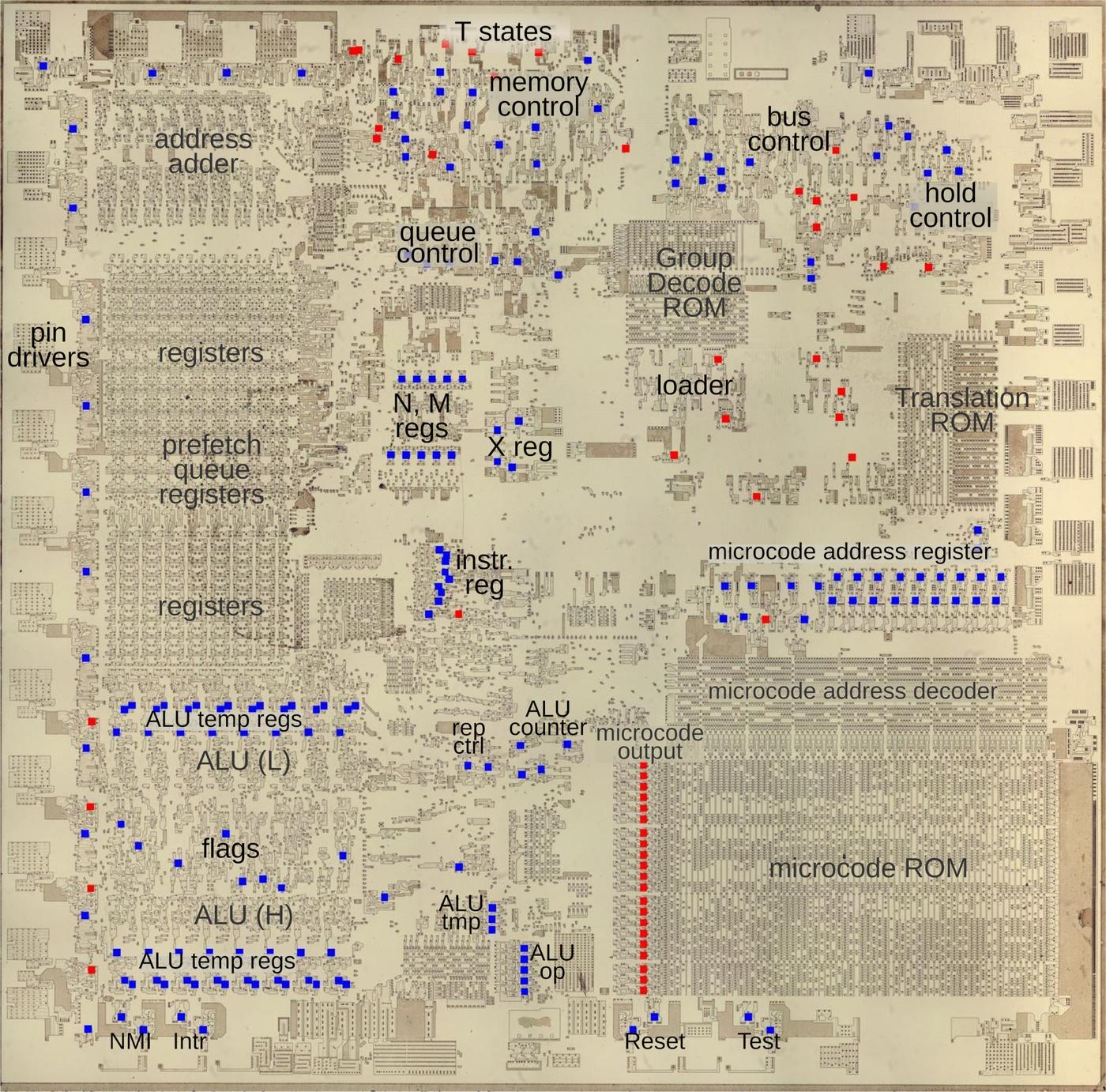
The die photo above shows the silicon die of the 8086.
In this image, I have removed the metal and polysilicon layers to show the silicon transistors underneath.
The colored squares indicate the flip-flops: blue flip-flops have an enable input, while red lack enable.
Flip-flops are used throughout the processor for a variety of roles.
Around the edges, they hold the state for output pins.
The control circuitry makes heavy use of flip-flops for various state machines, such as
moving through the "T states" that control the bus cycle.
The "loader" uses a state machine to start each instruction.
The instruction register, along with some special-purpose registers (N, M, and X) are built with
flip-flops.
Other flip-flops track the instructions in the prefetch queue.
The microcode engine uses flip-flops to hold the current microcode address as well as to
latch the 21-bit output from the microcode ROM.
The ALU (Arithmetic/Logic Unit) uses flip-flops to hold the status flags,
temporary input values, and information on the operation.
The flip-flop circuit
In this section, I'll explain how the flip-flop circuits work, starting with a basic D flip-flop.
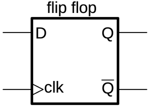
The D flip-flop (below) takes a data input (D) and stores that value, 0 or 1.
The output is labeled Q, while the inverted output is called Q (Q-bar).
This flip-flop is "edge triggered", so the storage happens
on the edge when the clock changes from low to high.4
Except at this transition, the input can change without affecting the output.
The 8086 implements most of its flip-flops dynamically, using pass transistor logic. That is, the capacitance of the wiring (in particular the transistor gate) holds the 0 or 1 state. The dynamic implementation is more compact than the typical static flip-flop implementation, so it is often used in processors. However, the charge on the capacitance will eventually leak away, just like DRAM (dynamic RAM). Thus, the clock must keep going or the values will be lost.3 This behavior is different from a typical flip-flop chip, which will hold its value until the next clock, whether that is a microsecond later or a day later.
The D flip-flop is built from two latch5 stages, each consisting of a pass transistor and an inverter.6
The first pass transistor passes the input value through while the clock is low. When the clock switches high,
the first pass transistor turns off and isolates the inverter from the input, but the value persists due to the capacitance (blue arrow).
Meanwhile, the second pass transistor switches on, passing the value from the first inverter through the second
inverter to the output.
Similarly, when the clock switches low, the second transistor switches off but the value is held by capacitance
at the green arrow.
(The circuit does not need an explicit capacitor; the wiring has enough capacitance to hold
the value.)
Thus, the output holds the value of the D input that was present at the moment when the clock switched from low to high.
Any other changes to the D input do not affect the output.
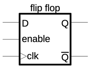
The basic flip-flop can be modified by adding an "enable" input that enables or blocks the clock.7
When the enable input is high, the flip-flop records the D input on the clock edge as before, but when the enable input is low, the flip-flop holds its previous value.
The enable input allows the flip-flop to hold its value for an arbitrarily long period of time.
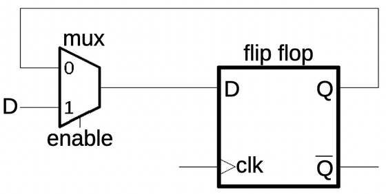
The enable flip-flop is constructed from a D flip-flop by feeding the flip-flop's output back to the input as shown below.
When the enable input is 0, the multiplexer selects the current Q output as the new flip-flop D input,
so the flip-flop retains its previous value.
But when the enable input is 1, the multiplexer selects the new D value.
(You can think of the enable input as selecting "hold" versus "load".)
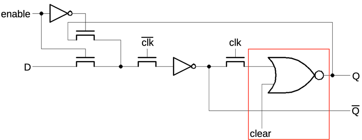
The multiplexer is implemented with two more pass transistors, as shown on the left below.8
When enable is low, the upper pass transistor
switches on, passing the current Q output back to the input. When enable is high, the lower pass transistor switches on,
passing the D input through to the flip-flop.
The schematic below also shows how the inverted Q' output is provided by the first inverter.
The circuit "cheats" a bit; since the inverted output bypasses the second transistor, this output can
change before the clock edge.
The flip-flops often have a set or clear input, setting the flip-flop high or low.
This input is typically connected to the processor's "reset" line, ensuring that the flip-flops are initialized
to the proper state when the processor is started.
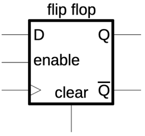
The symbol below shows a flip-flop with a clear input.
To support the clear function, a NOR gate replaces the inverter as shown below (red).
When the clear input is high, it forces the output from the NOR gate to be low.
Note that the clear input is asynchronous, changing the Q output immediately. The inverted Q output, however, doesn't change until
clk is high and the output cycles around.
A similar modification implements a set input that forces the flip-flop high: a NOR gate replaces the first inverter.
Implementing a flip-flop in silicon
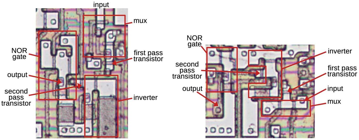
The diagram below shows two flip-flops as they appear on the die. The bright gray regions are doped silicon, the bottom layer of the chip The brown lines are polysilicon, a layer on top of the silicon. When polysilicon crosses doped silicon, a transistor is formed with a polysilicon gate. The black circles are vias (connections) to the metal layer. The metal layer on top provides wiring between the transistors. I removed the metal layer with acid to make the underlying circuitry visible. Faint purple lines remain on the die, showing where the metal wiring was.
Although the two flip-flops have the same circuitry, their layouts on the die are completely different. In the 8086, each transistor was carefully shaped and positioned to make the layout compact, so the layout depends on the surrounding logic and the connections. This is in contrast to modern standard-cell layout, which uses a standard layout for each block (logic gate, flip-flop, etc.) and puts the cells in orderly rows. (Intel moved to standard-cell wiring for much of the logic in the the 386 processor since it is much faster to create a standard-cell design than to perform manual layout.)
Conclusions
The flip-flop with enable input is a key part of the 8086, appearing throughout the processor.
However, the enable input is a fairly obscure feature for a flip-flop component;
most flip-flop chips have a clock input, but not an enable.9
Many FPGA and ASIC synthesis libraries, though, provide it, under the name
"D flip-flop with enable" or "D flip-flop with clock enable".
I plan to write more on the 8086, so follow me on Twitter @kenshirriff or RSS for updates. I've also started experimenting with Mastodon recently as @[email protected] so you can follow me there too.
Notes and references
-
Some early computers were asynchronous, such as von Neumann's IAS machine (1952) and its numerous descendants. In this machine, there was no centralized clock. Instead, a circuit such as an adder would send a pulse to the next circuit when it was done, triggering the next circuit in sequence. Thus, instruction execution would ripple through the computer. Although almost all later computers are synchronous, there is active research into asynchronous computing which is potentially faster and lower power. ↩
-
I'm focusing on the dynamic flip-flops in this article, but I'll mention that the 8086 has a few latches built from cross-coupled NOR gates. Most 8086 registers use cross-coupled inverters (static memory cells) rather than flip-flops to hold bits. I explained the 8086 processor's registers in this article. ↩
-
Dynamic circuitry is why the 8086 and many other processors have minimum clock speeds: if the clock is too slow, signals will fade away. For the 8086, the datasheet specifies a maximum clock period of 500 ns, corresponding to a minimum clock speed of 2 megahertz. The CMOS version of the Z80 processor, however, was designed so the clock could be slowed or even stopped. ↩
-
Some flip-flops in the 8086 use the inverted clock, so they transition when the clock switches from high to low. Thus, there are two sets of transitions in the 8068 for each clock cycle. ↩
-
The terminology gets confusing between flip-flops and latches, which sometimes refer to the same thing and sometimes different things. The term "latch" is often used for a flip-flop that operates on the clock level, not the clock edge. That is, when the clock input is high, the input passes through, and when the clock input is low, the value is retained. Confusingly, the clock for a latch is often called "enable". This is different from the
enableinput that I'm discussing, which is separate from the clock. ↩ -
I asked an Intel chip engineer if they designed the circuitry in the 8086 era in terms of flip-flops. He said that they typically designed the circuitry in terms of the underlying pass transistors and gates, rather than using the flip-flop as a fundamental building block. ↩
-
You might wonder why the clock and enable are separate inputs. Why couldn't you just AND them together so when
enableis low, it will block the clock and the flip-flop won't transition? That mostly works, but three factors make it a bad idea. First, the idea of using a clock is so everything changes state at the same time. If you start putting gates in the clock path, the clock gets a bit delayed and shifts the timing. If the delay is too large, the input value might change before the flip-flop can latch it. Thus, putting gates in the clock path is frowned upon. The second factor is that combining the clock and enable signals risks race conditions. For instance, suppose that theenableinput goes low and high while the clock remains high. If you AND the two signals together, this will yield a spurious clock edge, causing the flip-flop to latch its input a second time. Finally, if you block the clock for too long, a dynamic flip-flop will lose its value. (Note that the flip-flop circuit used in the 8086 will refresh its value on each clock even if theenableinput is held low for a long period of time.) ↩ -
A multiplexer can be implemented with logic gates. However, it is more compact to implement it with pass transistors. The pass transistor implementation takes four transistors (two fewer if the inverted enable signal is already available). A logic gate implementation would take about nine transistors: an AND-OR-INVERT gate, an inverter on the output, and an inverter for the enable signal. ↩
-
The common 7474 is a typical TTL flip-flop that does not have an
enableinput. Chips with an enable are rarer, such as the 74F377. Strangely, one manufacturer of the 74HC377 shows the enable as affecting the output; I think they simply messed up the schematic in the datasheet since it contradicts the function table.Some examples of standard-cell libraries with enable flip-flops: Cypress SoC, Faraday standard cell library, Xilinx Unified Libraries, Infineon PSoC 4 Components, Intel's CHMOS-III cell library (probably used for the 386 processor), and Intel Quartus FPGA. ↩
