The digital ranging system that measured the distance to the Apollo spacecraft

During the Apollo missions to the Moon, a critical task for NASA was determining the spacecraft's position. To accomplish this, they developed a digital ranging system that could determine the distance to the spacecraft, hundreds of thousands of kilometers away, with an accuracy of about 1 meter.

The basic idea was to send a radio signal to the spacecraft and determine how long it takes to return. Since the signal traveled at the speed of light, the time delay gives the distance. The main problem is that due to the extreme distance to the spacecraft, a radar-like return pulse would be too weak.2 The ranging system solved this in two ways. First, a complex transponder on the spacecraft sent back an amplified signal. Second, instead of sending a pulse, the system transmitted a long pseudorandom bit sequence. By correlating this sequence over multiple seconds, a weak signal could be extracted from the noise.1

In this blog post I explain this surprisingly-complex ranging system. Generating and correlating pseudorandom sequences was difficult with the transistor circuitry of the 1960s. The ranging codes had to be integrated with Apollo's "Unified S-Band" communication system, which used high-frequency microwave signals. Onboard the spacecraft, a special frequency-multiplying transponder supported Doppler speed measurements. Finally, communicating with the spacecraft required a complex network of ground stations spanning the globe.

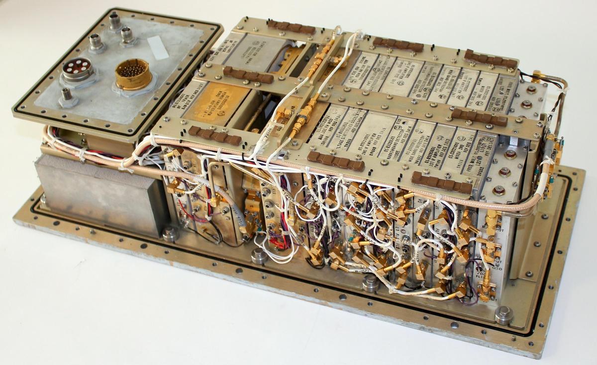
The Apollo Service Module's transponder with the lid removed, showing the circuitry inside. The transponder returned the ranging signal to Earth, multiplying the frequency by exactly 240/221.

The Apollo Service Module's transponder with the lid removed, showing the circuitry inside. The transponder returned the ranging signal to Earth, multiplying the frequency by exactly 240/221.

The ranging system

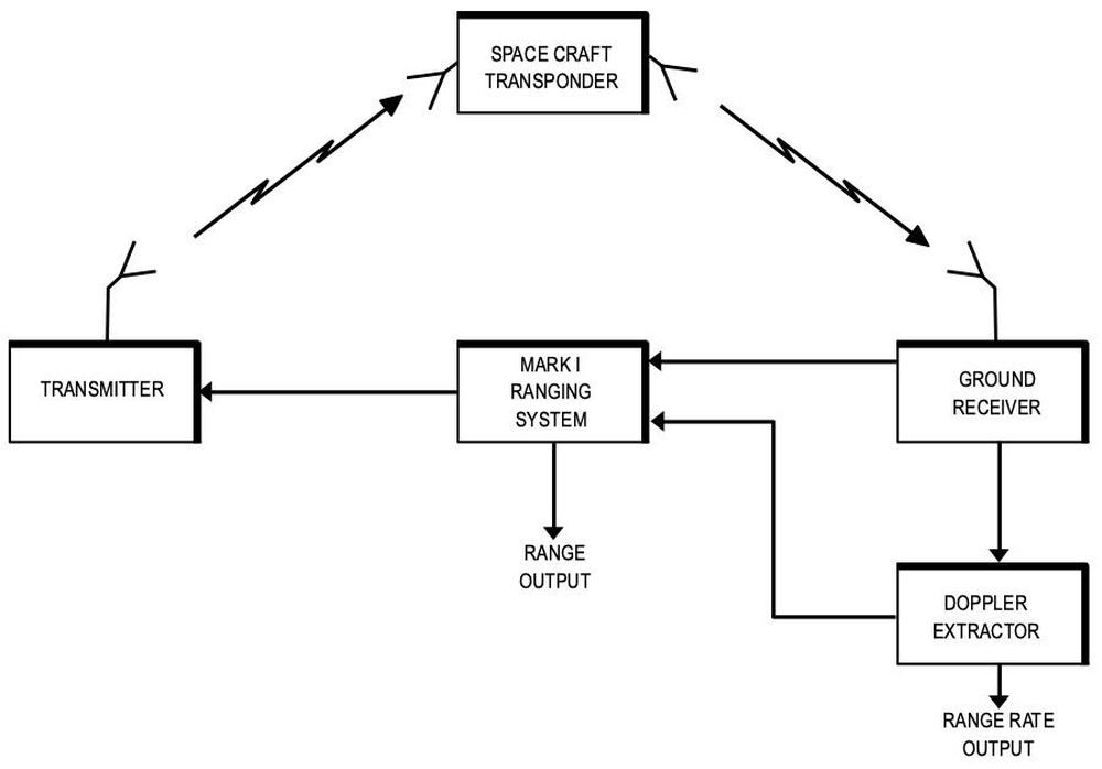
The ranging system measured how long a signal takes to travel to the spacecraft and back.3 As shown below, the ranging system transmitted a pseudorandom bit sequence to the spacecraft. The spacecraft's transponder returned the signal to the ground receiver. The returned signal was correlated against the original signal to determine the time shift, and thus the distance. Meanwhile, a Doppler measurement (described later) provided the speed of the spacecraft.4

Block diagram of the Apollo ranging subsystem. Redrawn from A study of the JPL Mark I ranging subsystem

Block diagram of the Apollo ranging subsystem. Redrawn from A study of the JPL Mark I ranging subsystem

The key step was to correlate the transmitted and received signals to determine the time delay. When the two signals were aligned with the proper delay, the bits matched. Because the sequence is pseudorandom, if the two signals were misaligned, the bits didn't match (except randomly).5 Thus, by testing how many bits match (i.e. the correlation) for different delays, the proper delay could be determined. Since the signals could be correlated over long time intervals (multiple seconds), the range could be determined even if the signal was extremely weak and hidden by noise.

The code sequence needed to be very long in order to unambiguously determine the range; the system uses a pseudorandom sequence that is 5,456,682 bits long. Since the code is sent at 1 megahertz, it repeats every 5.46 seconds. A radio signal can travel 800,000 kilometers and back in this time, while the Moon is about 384,000 kilometers away, so the system can unambiguously measure over twice the distance to the Moon. Note that at one megahertz, one bit of the signal corresponds to 150 meters of range. The system achieved more accuracy by comparing the phase of the signals.

Conceptually, the transmitted and received sequences were shifted until they match, and the amount of shift gave the delay, and thus the distance. However, it's impractical to try 5 million different shifts to match the sequence, especially with the technology of the 1960s. To solve the matching problem, the sequence was constructed from several shorter codes, from 2 to 127 bits long. These "sub-codes" were short enough that they could be matched by brute force. The overall delay could then be determined by the delays of the sub-codes. The system used four sub-codes—sub-code A had a length of 31 bits, B was 63 bits, C was 127 bits, and X was 11 bits—along with a two-valued clock CL. Since these lengths are relatively prime, the combined sequence has an overall length equal to the product: 5,456,682. The important concept is that a very long code could be generated and matched using hardware, since the sub-codes were short.

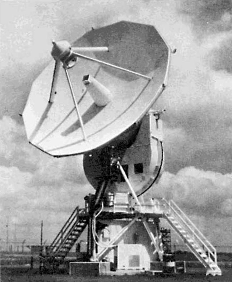
A 30-foot antenna. From Apollo Unified S-Band Technical Conference.

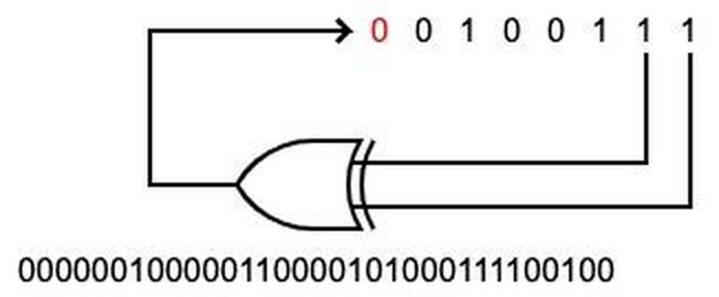
I made an interactive page that demonstrates how the sub-code sequences were created. The sub-code sequences of lengths 31, 63, and 127 were generated with a well-known technique called the linear-feedback shift register (LFSR). In this technique, a shift register of length N holds bits. In each step, a new bit is generated from the exclusive-or of two bits in the shift register. The new bit is shifted in, and an old bit is shifted out, providing a code bit. This technique can generate a pseudorandom sequence of length 2N-1 with good statistical properties. In order to generate a sub-code of length 11, the X codes were generated from a Legendre sequence.7

The C sub-code is generated from a 7-bit delay line (black). The last two bits are fed into an XOR gate to produce a new bit (red). Part of the pseudorandom sequence is shown below the gate.

The C sub-code is generated from a 7-bit delay line (black). The last two bits are fed into an XOR gate to produce a new bit (red). Part of the pseudorandom sequence is shown below the gate.

Combining the sub-codes to form the overall code isn't as straightforward as you might think, since each sub-code must be individually recognizable in the result. The A, B, and C sub-codes were combined with the majority function maj(A,B,C), which returns the most common bit out of the three inputs.6 The complete formula for the bit sequence was (X·maj(A,B,C))⊕CL.

Construction of the ranging system

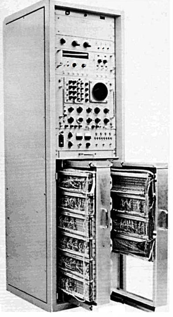
The ranging process was implemented by the "Mark I ranging subsystem" below. Although this was called a "special-purpose binary digital computer", it's not really a computer in the modern sense, but more of a state machine that moved through the necessary steps. First, the ground station sent the code sequence to the spacecraft and synchronized to the received signal. Next, the ranging system tested the different offsets for the X sub-code and found the offset with the best correlation. It repeated the process for the A, B, and C sub-codes. The digital circuitry performed some tricky modulo arithmetic8 to compute the range from the sub-code offsets. Finally, the Doppler subsystem determined the spacecraft's speed and constantly added this to the range to keep the range up to date as the spacecraft moved. I've made an interactive page that demonstrates these steps.

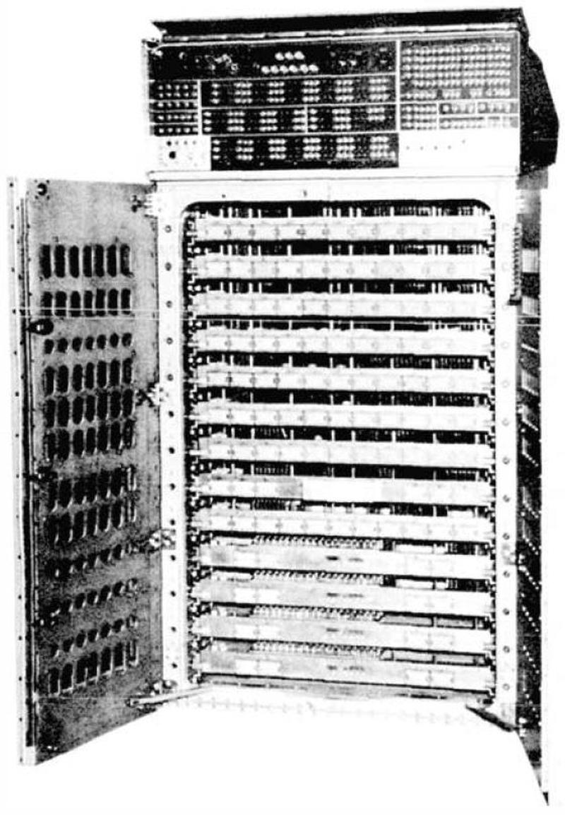
The Mark I ranging subsystem. From Apollo Unified S-Band System.

The Mark I ranging subsystem. From Apollo Unified S-Band System.

The ranging system was built from "T-Pac modules", boards that used transistors and other discrete components to build simple digital components such as logic gates and flip flops.9 The T-Pac modules were introduced by Computer Control Company in 1958 and were designed for quick and efficient implementation of a digital system, running at 1 MHz. Groups of 32 T-Pac cards were mounted in a "T-BLOC" rack-mounted chassis, and 10 T-BLOCs were installed in two racks. The cards were connected by plugging wires and taper pins into a large grid.

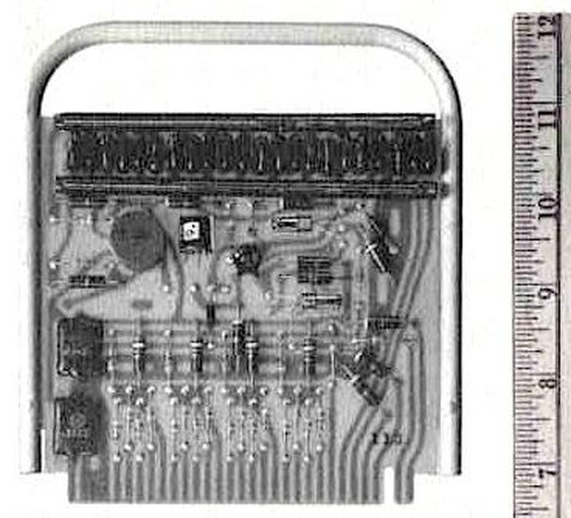
One module was the T-Pac LE-10 "logic element" module, below, implementing four AND gates. It cost $98 in 1961 (about $700 in current dollars), showing how expensive digital logic was at the time. The ranging system used about 300 digital modules, so the digital circuitry for ranging would have cost hundreds of thousands of (current) dollars, a cost repeated at each ground station.

A T-Pac module. This is the LE-10 "logic element".

A T-Pac module. This is the LE-10 "logic element".

Tasks that we nowadays consider trivial were difficult with the technology of the time. For instance, the range was stored as a 31-bit binary value. But instead of a register, the value was stored in a magnetorestrictive delay line, as torsion pulses in a long nickel wire. To add a value to the range, the circuitry used a single-bit serial adder, adding bits one at a time as they exited the nickel wire, and then cycling the bits back into the wire.

One interesting circuit is the correlation level detector that tests for correlation between a particular sub-code and the received signal. The correlation started as an analog voltage, which was converted to a digital value by a "Voldicon. The correlation was integrated over time by summing the binary values using another 31-bit storage/adder circuit. The number of summed samples could range from 1 to 219 samples, user-settable through "Digiswitch" thumbwheel switches. By integrating the correlation over a long time interval, an extremely weak signal could be detected in the presence of noise. The system kept track of the best offset, storing the value in another delay line. The total ranging time varied from 1.6 seconds for a strong signal to 30 seconds at lunar distance.

Determining the speed with Doppler

The ranging system could also measure the spacecraft's speed by measuring the Doppler shift of the returned signal. If the spacecraft was moving away from Earth, the waves would be stretched out, lowering the frequency. Conversely, the frequency would increase if the spacecraft was moving towards Earth.10 By measuring the frequency shift, the spacecraft's speed could be accurately determined.12

A moving source causes the wavelength to be decreased if the source is moving closer or increased if the source is moving away. Diagram by Tkarcher.

A moving source causes the wavelength to be decreased if the source is moving closer or increased if the source is moving away. Diagram by Tkarcher.

The Doppler measurement impacted the radio system's design in two ways. First, the spacecraft couldn't simply receive and retransmit the signal, because the Doppler shift from the upwards journey would be lost. Instead, a complex frequency-multiplying transponder system was used, so the downlink signal's frequency was exactly 240/221 times the received uplink frequency.11 Second, the spacecraft used phase modulation (PM) instead of the common frequency modulation (FM) for most communication: since frequency modulation changes the signal's frequency, it would have interfered with the Doppler measurements.

The Apollo radio system

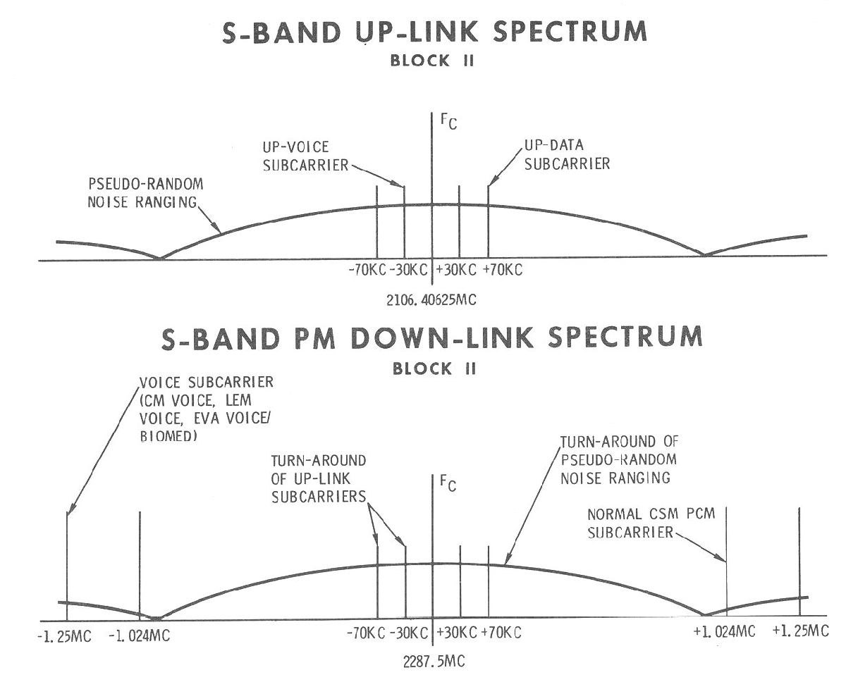
Apollo used a complex radio system called the Unified S-Band System that included voice, telemetry, scientific data, television, and the ranging data. These signals were combined and transmitted over a single carrier frequency in the S-band frequency range. The diagrams below show how the spectrum was allocated for the signal up to the spacecraft (transmitted at 2.10640625 GHz), and the down-link spectrum at 2.2875 GHz. These two frequencies are in the exact ratio of 240/221, which turns out to be important. Notice that the voice and data are on fairly narrow subcarriers, while the pseudorandom ranging data has a lower, but very wide spectrum. (The ranging signal looks a lot like white noise due to its randomness.) The wide spectrum makes the ranging signal easier to detect at low levels with noise. Even though the ranging spectrum overlaps with the voice and data subcarriers, they don't interfere too much because the ranging spectrum is spread out.

The spectrum used by the Apollo radio system.

The spectrum used by the Apollo radio system.

The transponder

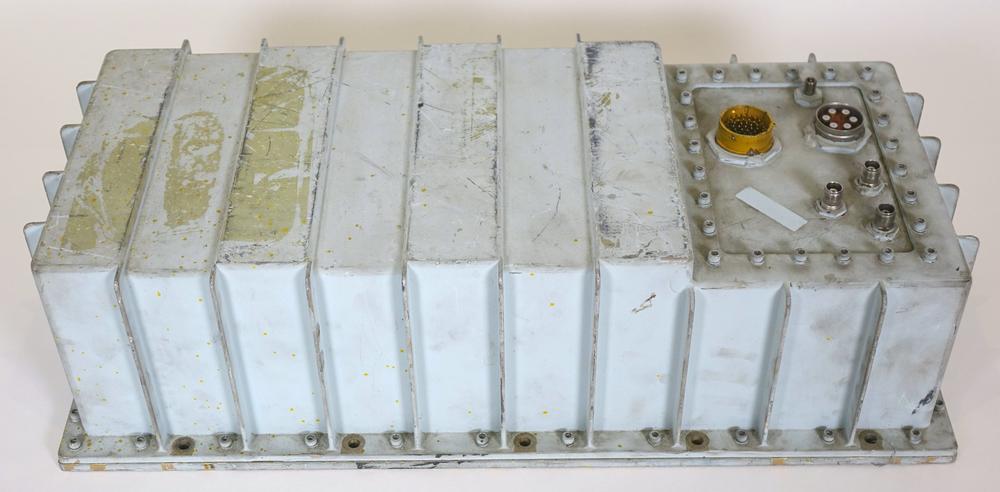
The S-band transponder onboard the spacecraft had a critical role in both ranging and for communications in general. From the outside, the transponder (built by Motorola) is a plain blue-gray box, weighing about 32 pounds. The connectors at the right linked the transponder to other parts of the radio system. Internally, the transponder was crammed full of radio circuitry: phase modulators for voice data, a detector for received uplink data, and an FM transmitter for video.14

The S-band transponder.

The S-band transponder.

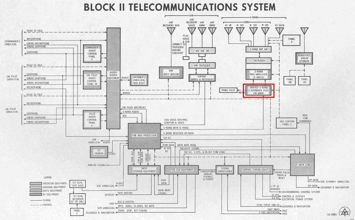
The block diagram below shows the role of the transponder (red) in the communications system. Once the spacecraft was outside of VHF range (about 1500 miles), all communication used the S-band and went through the transponder. The transponder was connected to a traveling-wave tube amplifier and then the spacecraft's antennas.

Diagram of the communications system used in Apollo. The transponder is highlighted in red. Click this (or any image) for a larger version.
From "Apollo Logistics Training", courtesy of Spaceaholic.

Diagram of the communications system used in Apollo. The transponder is highlighted in red. Click this (or any image) for a larger version. From "Apollo Logistics Training", courtesy of Spaceaholic.

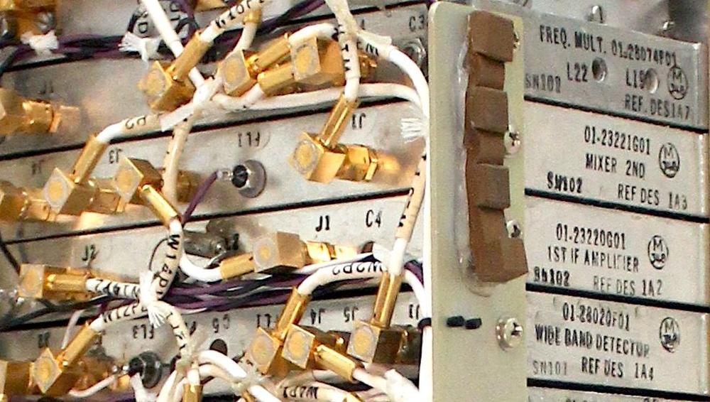
The photo below shows a closeup of the circuitry inside the transponder. The transponder is constructed of multiple modules, connected by tiny coaxial cables. The frequency multiplier, mixer, IF amplifier, and wide band detector modules are visible. Most of the modules are duplicated on the other side of the transponder to provide redundancy, since a failure of the transponder would jeopardize the mission.

Closeup of the transponder.

Closeup of the transponder.

The most complex part of the transponder is how it received the ranging data from Earth and echos it back. To avoid interference, the retransmitted data is at a different frequency from the received data. But in order to preserve the Doppler shift information, the transmitted frequency had to vary with the received frequency, so it couldn't be fixed. Instead, the transponder multiplied the received frequency by exactly 240/221 to generate the retransmission frequency, using a complex phase-locked loop circuit.

A phase-locked loop is a widely-used circuit that allows an oscillator to be locked to another frequency source, even in the presence of noise. It uses a voltage-controlled oscillator whose output is compared to the input. If the output is falling behind, the oscillator is sped up. If the input is falling behind, the oscillator is slowed down. Eventually, the oscillator will lock onto the input signal and will track it. The transponder uses a more complex circuit, so the output frequency tracks a multiple of the input frequency, specifically the output frequency is 240/221× the input (uplink) frequency.15

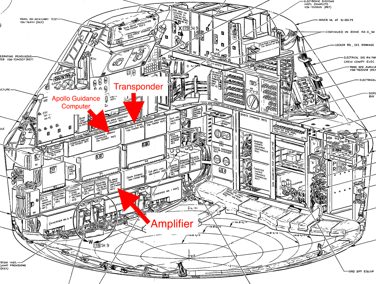
The transponder was one of many electronics boxes crammed into the Command Module. The diagram below shows its position in the equipment racks.

This diagram of the Apollo Command Module shows the position of the S-band transponder, along with the traveling-wave-tube amplifier and the Apollo Guidance Computer.

This diagram of the Apollo Command Module shows the position of the S-band transponder, along with the traveling-wave-tube amplifier and the Apollo Guidance Computer.

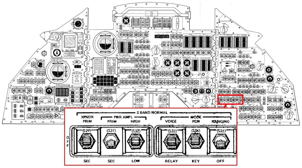
The console of the Command Module (below) was extremely complicated, with many controls and switches. The astronauts used the highlighted switches to control the transponder and to turn ranging on and off.

Astronauts controlled ranging through a switch on the console. Diagram from Command/Service Module Systems Handbook p208.

Astronauts controlled ranging through a switch on the console. Diagram from Command/Service Module Systems Handbook p208.

Ground stations

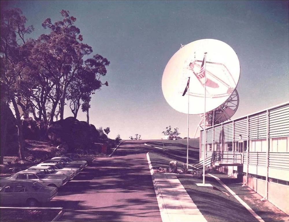
Communication with Apollo required powerful ground stations with large antennas.17 These stations needed to be situated around the world to maintain constant communication with Apollo as the Earth rotated. The three main stations had 85-foot (26-meter) parabolic antennas and were located in Goldstone, California; Canberra, Australia; and Madrid, Spain, part of the Manned Space Flight Network (MSFN). Other stations had smaller 30-foot antennas. Coverage gaps were filled by special ships with 30-foot antennas as well as special Apollo Range Instrumentation Aircraft (ARIA), based on C-135 cargo aircraft.

NASA's 26-meter antenna at Honeysuckle Creek, Australia. Photo from NASA.

NASA's 26-meter antenna at Honeysuckle Creek, Australia. Photo from NASA.

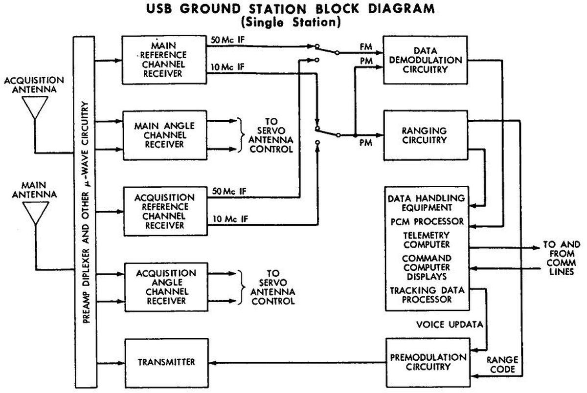
The block diagram below gives a hint of the complexity of a ground station, with signal processing equipment as well as computers16 and networking to Mission Control and other sites. The "Ranging Circuitry" block has the most relevance to this discussion, but I'd also like to point out the "angle channel receivers". The antennas were servo-positioned to lock onto the spacecraft's signal. This provided an angle measurement of the spacecraft's position, which was combined with the range to yield the spacecraft's 3-D position in space.

Block diagram of a Unified S-Band ground station. From Apollo Unified S-Band System.

Block diagram of a Unified S-Band ground station. From Apollo Unified S-Band System.

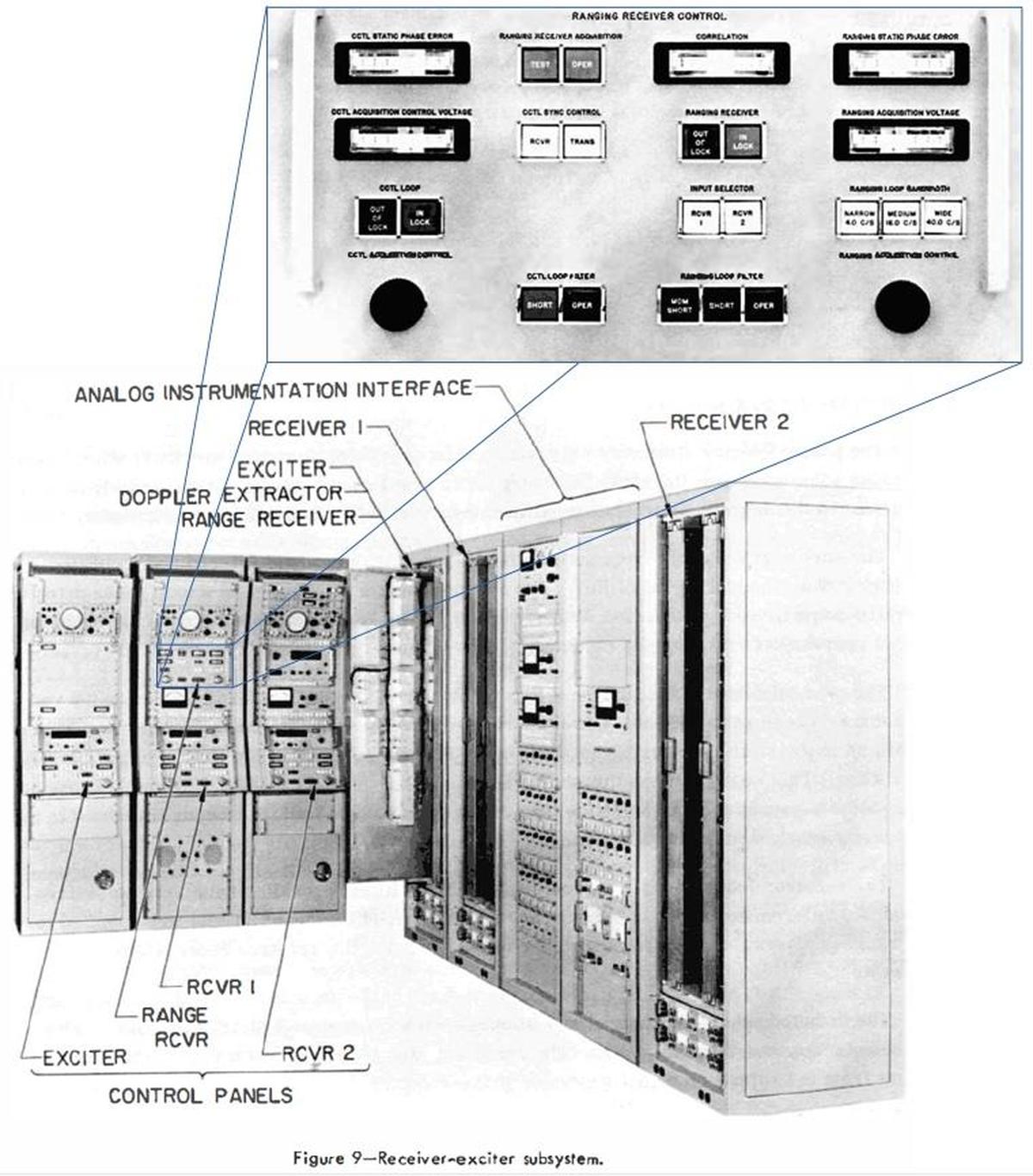
The photo below shows the ground station's transmitter/receiver cabinets that handled the unified S-Band signals. These cabinets were the connection between the microwave equipment (amplifiers and antennas) and the radio-frequency subsystems for voice, data, instrumentation, ranging, and so forth. The photo zooms in on the ranging receiver control panel. This ranging circuitry performed the analog tasks: it demodulated the received ranging signal, tracked the frequency, extracted the clock and the Doppler signal, and measured the correlation. These signals were provided to the digital ranging subsystem described earlier.

The receiver-exciter subsystem of the ground station, with a closeup of the ranging receiver. From Apollo Unified S-Band System.

The receiver-exciter subsystem of the ground station, with a closeup of the ranging receiver. From Apollo Unified S-Band System.

Conclusion

The ranging system provided the distance to the spacecraft, the Doppler provided the spacecraft's (radial) velocity, and the position of the receiving antenna provided the spacecraft's angular position. The system provides a great deal of accuracy for distance and speed: 1.5-meter range resolution and 0.1 meter/sec speed resolution. Because the angular measurement depended on the physical positioning of the antenna, angular resolution was much worse: 0.025°, which corresponds to over 150 kilometers at the distance of the Moon.

The ranging system illustrates the complexity of Apollo. Even though ranging was a small part of Apollo's navigation, it required complex racks of hardware distributed to sites around the world, specialized algorithms, and an advanced transponder onboard the spacecraft. Almost every part of Apollo has this sort of fractal complexity, where a seemingly-simple requirement such as finding the distance to the spacecraft required numerous innovations. The S-band communication system alone required a 1965 conference with 317 pages of proceedings.

The ranging system is hard to understand from a text description, so I've made two interactive pages that demonstrate it. The first page shows how linear-feedback shift registers (LFSR) and XOR gates generate the subcodes, and how the subcodes create the transmitted signal. The second page shows how the correlations are determined for the various subcodes and how the range is computed from these values.

I've implemented the ranging codes on a Teensy, so the next step is to transmit the codes through an actual Apollo transponder. I announce my latest blog posts on Twitter, so follow me @kenshirriff for updates. I also have an RSS feed. Thanks to Steve Jurvetson for providing the S-band transponder and the traveling-wave tube amplifier. Thanks to Mike Stewart for extensive information on the Apollo hardware and CuriousMarc for driving the transponder restoration.

Notes and references

  1. The ranging system has a lot in common with GPS. GPS also works by sending a pseudorandom bit sequence and using correlation to determine the signal's delay. There are several important differences though. First, ranging only determined distance, while GPS determines position in three dimensions and also the exact time. (This is why GPS requires visibility of at least four satellites.)

    Second, the GPS signal is transmitted from a satellite and received on the ground, unlike the Apollo ranging signal which was both transmitted and received on the ground. As a result, the GPS receiver doesn't have the transmitted signal available, but must generate its own copy for comparison.

    Third, GPS satellites are about 20,000 kilometers from Earth, while the Moon is 384,000 kilometers from Earth, making the Apollo signal much weaker. (Although Apollo did have the advantage of huge 26-meter receiving antennas, rather than a GPS antenna that is a few centimeters long.)

    Finally, GPS has the advantage of complex integrated circuits to determine the correlation, rather than racks full of transistor logic.

    As far as I can tell, there isn't any direct connection between the Apollo ranging system and GPS. GPS grew out of the Transit (Naval Navigation Satellite System), the Timation satellite program, and USAF Project 621B (history). 

  2. A radar signal was first bounced off the Moon in 1946 (details, p 25), but the distance accuracy was only ±1000 miles. The radar return from the spacecraft would be much smaller due to its size. 

  3. There's a complicated history leading up to the Apollo ranging system. Development of Radar (RAdio Detection And Ranging) started in the 1920s. Radar became critically important in World War II, and to counteract jamming, spread-spectrum ideas were applied. The WHYN missile ranging system (1946) used correlation detection to determine the phase difference and thus range. The Federal Telecommunications Laboratories investigated noise-like signals for communication in 1948. This unusual system stored noise values optically on a rotating disk; curiously, the original source of random numbers was the Manhattan telephone directory. The NOMAC (NOise Modulation And Correlation) system (1952) explored thermal noise as a carrier for communication. The CODORAC (either COded DOppler Ranging And Command or COded Doppler RAdar Command) system at JPL (1952) used similar electronics and became the basis for the Deep Space Instrumentation Facility. It introduced a phase-locked loop (PLL) to cancel out Doppler variations, as well as linear-feedback shift register sequences for "pseudonoise". JPL's continuing research led to the ranging system used for Apollo, as well as the Space Ground Link Subsystem (SGLS) (1966), which is still used by the US Air Force. See The Origins of Spread-Spectrum Communications for more. 

  4. One complication is that the spacecraft is moving very rapidly during the ranging process, up to 10,000 meters per second. This creates two problems. First, the distance measurement will be out of date by the time it is completed. Second, the bit alignment is shifting many times per second, which makes it hard to find the correlation. The solution was to use separate clocks for the sending and receiving circuitry. The receiver clock was locked onto the signal received from the spacecraft. (Due to Doppler shift, this frequency would be slightly different.) By generating the codes from this clock, the codes stayed exactly aligned even as the spacecraft moved. Integrating the difference between the two clocks provided the change in distance since the start of the measurement. Thus, the computed range remained locked to the distance at the start of the measurement, and the Doppler data gave the incremental distance change. Combining these provided the correct range, continuously updated. 

  5. The pseudorandom sequence must be carefully designed so non-matches can be clearly distinguished from matches, even in the presence of noise. Specifically, misalignments should have as many mismatched bits as possible. The LFSR and Legendre sequences provided this property. In contrast, the sequence 0000011111 would be a bad choice, since if it is shifted by 1, most of the bits still match. Moreover, the number of mismatches should be constant, regardless of the shift. Otherwise, the correlation may match against a local peak rather than the correct shift.

    For more about the mathematics of correlating codes, see Sequences with Small Correlation 

  6. The majority function maj(A,B,C) matches the A value 75% of the time (and likewise for B or C), allowing the correlation to be detected. (In contrast, A⊕B⊕C would be a bad choice since it only matches A 50% of the time, so the correlation is essentially random.) For a quick analysis of the majority function, consider maj(A,B,C) where A is 1 and the other inputs have four possibilities: maj(1,0,0)=0, maj(1,0,1)=1, maj(1,1,0)=1, and maj(1,1,1)=1. The result matches a for all except the first case, i.e. 75% of the time. (If a is 0, the analysis is similar.) The majority function can be expressed in Boolean logic as A·B+B·C+A·C, i.e. true if any two inputs are set. 

  7. The idea of the Legendre sequence is that some numbers have an integer "square root" modulo 11 (technically a quadratic residue), and some do not. For instance, 52 = 25 ≡ 3 modulo 11, so in a sense 5 is the square root of 3. If you take the numbers 0 through 10 and assign 1 if the number has a "square root" and 0 otherwise, you get the X codes. (The ranging sequence is slightly different from the mathematical Legendre sequence, which uses -1 for a "quadratic nonresidue" instead of 0.) 

  8. The modulo equations were solved using the Chinese remainder theorem, developed by the Chinese mathematician Sunzi Suanjing in the third century. The ranging system used pre-computed numbers that canceled out for all except one sub-code. For instance, 992124 is congruent to 1 modulo 11, but congruent to 0 modulo 31, 63, and 127. Multiplying this number by the X offset provides the X sub-code's contribution to the range.

    The Chinese remainder theorem constants are
    992124 ≡ 1 (mod 11) for the X subcode
    1408176 ≡ 1 (mod 31) for the A subcode
    736219 ≡ 1 (mod 63) for the B subcode
    2320164 ≡ 1 (mod 127) for the C subcode
    These numbers are ≡ 0 modulo the other cases. Thus, the total offset T = 992124×X + 1408176×A + 736219×B + 2320164×C (mod 5,456,682).

    The numbers can be obtained by a straightforward algorithm, described in Appendix E of the NASA document. The numbers were hard-coded into the ranging hardware by a "Chinese Number Generator", logic gates that provided the numbers in serial form for serial addition. 

  9. The Honeywell DDP-116 minicomputer (1965) also used T-Pac modules. Honeywell acquired Computer Control Co., the manufacturer of T-Pacs, in 1966 to expand their digital capability. The earlier Honeywell DDP-19 was a curious computer since it used 19-bit words; it was built with S-Pac modules. The later µ-Pac modules used integrated circuits in place of transistors. 

  10. Note that the Doppler system can only measure the spacecraft's velocity towards or away from Earth. Perpendicular motion would not show up. 

  11. I haven't been able to find any explanation for the specific 240/221 frequency ratio between the transmitted and received frequencies. The two frequencies needed to be different so the transmitted signal doesn't overpower the received frequency. The ratio should be fairly close to 1, though, so the system can be optimized for a particular frequency band. The ratio should be reasonably small integers so frequency multipliers can be used. But the mystery to me is why 240/221 instead of, say, 12/11, which is almost the same but much easier to generate. My current theory is that the larger ratio avoided collisions between harmonics that would otherwise occur. (e.g. 12×f1 = 11×f2, which might distort the received signal?) 

  12. The code delay and the Doppler shift aren't independent, but are really two aspects of the same thing. For example, suppose the spacecraft is moving away at 15 meters/second. This will stretch the radio waves, decreasing the frequency. The 1 MHz pseudorandom signal transmitted to the spacecraft will return with each 1-microsecond interval stretched by 0.1 picoseconds.13 In 10 seconds, the ranging system will transmit 10 million pulses, so the Doppler stretching will cause the pulse train to be 1 microsecond longer, one pulse. The other way of looking at this is that after 10 seconds, the spacecraft will be 150 meters further away, increasing the round-trip signal delay by 1 microsecond. The signal delay from the Doppler shift is the same as the signal delay from the change in range because they are both caused by the spacecraft's motion. 

  13. Note that the signal transmitted from the ground will be Doppler-shifted when received by the spacecraft, and then the spacecraft's signal will be Doppler-shifted again when received on Earth, so the total Doppler shift is doubled. 

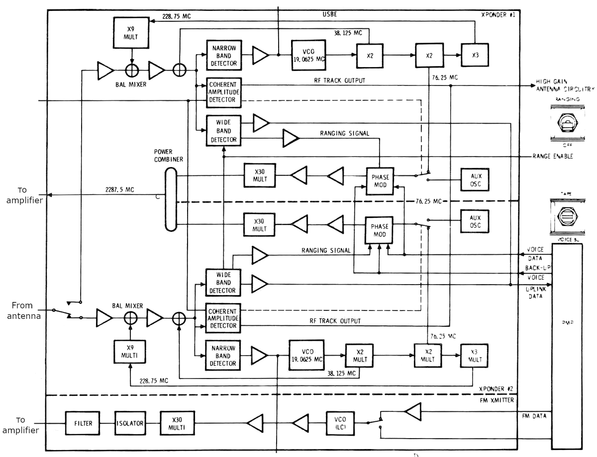
  14. The block diagram below shows the main components of the transponder. It consists of two phase-modulation transmitter/receivers (for redundancy). At the bottom is the FM transmitter for television signals (not redundant). The VCO (voltage-controlled oscillator) is phase-locked to the input signal, but multiplies the frequency by 240/221. This multiplication is done through several frequency multipliers and mixers. The ranging signal is extracted, phase-modulated at the new frequency, and sent to the antenna for transmission back to Earth.

    Block diagram of the transponder. (Click for a larger version.)

    Block diagram of the transponder. (Click for a larger version.)


  15. The transponder multiplies the received carrier frequency by 240/221. The Command Module used an uplink frequency of 2106.4 MHz, multiplied by 240/221 for the downlink frequency of 2287.5 MHz, although this can vary by ±120 kHz due to Doppler shift. The Lunar Module and Saturn rocket used an uplink carrier of 2101.8 MHz, multiplied by 240/221 for the downlink carrier of 2282.5 MHz.

    The 240/221 ratio was obtained by a complex process of mixers and frequency multipliers, as shown in the block diagram above. A voltage-controlled oscillator (VCO) in the transponder, ran at a frequency of approximately 19.0625 MHz and formed part of the phase-locked loop. The VCO signal was multiplied by 108 (12×9 in two steps) and mixed with the uplink signal received from Earth. The mixer yielded a signal whose frequency was the difference between the ground signal and the multiplied VCO signal, approximately 47.65625 MHz. A second mixer mixed this signal with two times the VCO frequency, yielding a signal at the difference frequency 9.53125 MHz. The VCO was then phase-locked to this signal to produce an output at twice its frequency, yielding the 19.0625 MHz VCO frequency. Putting this all into an equation:
    (Uplink - 108×VCO - 2×VCO)×2 = VCO
    which simplifies to VCO frequency = Uplink frequency * 2 / 221.

    Meanwhile, the transponder's transmitter multiplied the VCO frequency by 4 to yield a 76.25 MHz carrier. This was multiplied by 30 to yield the 2287.5 MHz downlink frequency. In other words, the VCO frequency was multiplied by 120 to transmit, so the transmitting frequency is 240/221 × Uplink frequency. Thus, the 240/221 frequency ratio is established by multiple frequency multipliers and mixers.

    But how was frequency multiplication implemented? Based on other Apollo circuits, I think the signal was fed into a step recovery diode, a special diode with very fast switching. This turned each input cycle into a sharp pulse, full of harmonics at multiples of the input frequency. A resonant network concentrated the energy at the desired harmonic, and then a filter removed unwanted frequency sidebands. The frequency of the resulting signal was at the desired multiple of the input signal. This process is described in Hewlett-Packard application note 920 (1968).  

  16. The ground stations used Univac 642B computers, a 30-bit computer with 32-kilowords of magnetic core storage. The computer was designed for military real-time applications. This computer was a key component of the Naval Tactical Data System, a groundbreaking 1960s system to manage combat information on US Navy ships.

    The Univac 624B computer. From Apollo Unified S-Band System.

    The Univac 624B computer. From Apollo Unified S-Band System.


  17. For details on the S-band system and ground stations, see Apollo Unified S-Band System. See A study of the JPL Mark I ranging subsystem for a detailed discussion of the ranging hardware. 

Reverse-engineering the LM185 voltage reference chip and its bandgap reference

Many circuits, such as a computer power supply or a phone charger, require a stable voltage reference, but it's harder than you might expect to keep a voltage stable when the temperature changes. One integrated circuit that does this is the LM185.1 I looked at the die of this chip and found some interesting features. The same silicon die is used for three different integrated circuits, using tiny internal fuses to change its functionality. The chip uses a special circuit called the bandgap reference to keep the voltage stable even if the temperature changes. In this blog post, I'll discuss the circuitry of the LM185 and its implementation in silicon.

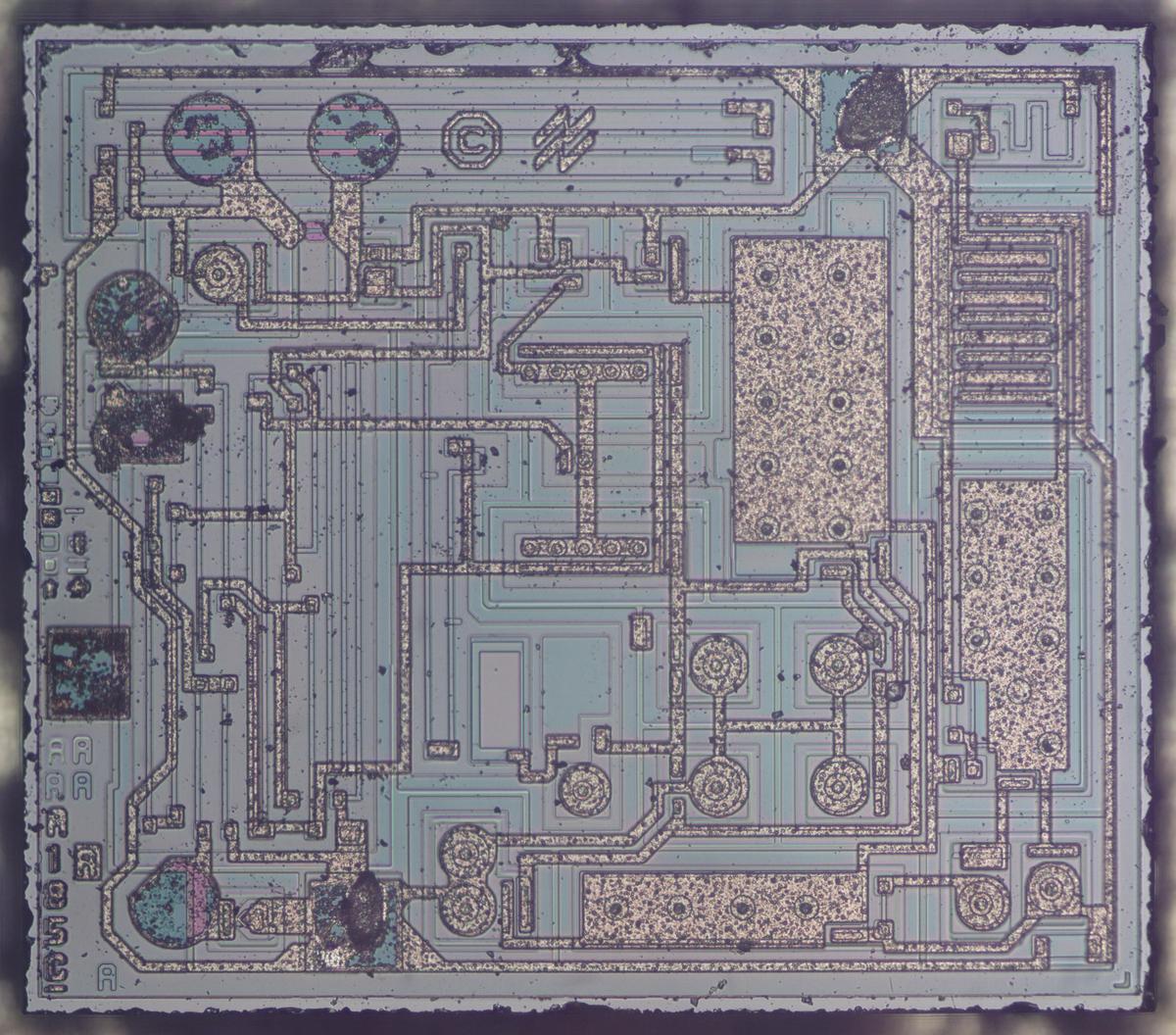
Composite die photo of the LM185. Click this (or any other) image for a larger version.

Composite die photo of the LM185. Click this (or any other) image for a larger version.

The photo above shows the LM185 die under the microscope, a tiny square of silicon. The underlying silicon is blue-gray, while the metal wiring on top is orangish. Regions of the silicon are doped with various impurities to form the transistors, resistors, and other devices on the chip. The variations in doping are visible as slight color changes in the silicon. At the top is the National Semiconductor logo.

The LM185 is available in three variants. The LM185-ADJ is the adjustable voltage reference. It has three pins: one is a feedback pin that controls the voltage. The LM185-1.2-N is a two-pin device, called a "micropower voltage reference diode". It is similar to a Zener diode providing 1.235V, but with better performance. (Lower power consumption, less noise, and better stability.) Finally, the LM185-2.5-N provides a 2.5V reference. The three variants are based on the same silicon die. The latter two have the feedback wired internally to provide a fixed voltage rather than an adjustable voltage.

The next sections describe how the various components of the chip are fabricated from silicon, and how they appear on the die.

NPN transistors

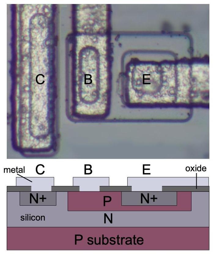
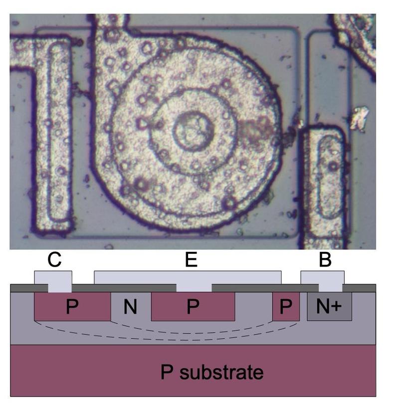
The photo below shows a closeup of one of the transistors in the LM185. The black lines and slightly different tints in the silicon indicate regions that have been doped to form N and P regions. The whitish areas are the metal layer of the chip on top of the silicon—these form the wires connected to the collector, emitter, and base.

Structure of an NPN transistor on the die. I edited the transistor layout so a cross-section would work.

Structure of an NPN transistor on the die. I edited the transistor layout so a cross-section would work.

Underneath the photo is a cross-section drawing illustrating how the transistor is constructed. There's a lot more than just the N-P-N sandwich you see in books, but if you look carefully at the vertical cross-section below the 'E', you can find the N-P-N that forms the transistor. The emitter (E) wire is connected to N+ silicon. Below that is a P layer connected to the base contact (B). And below that is an N+ layer connected (indirectly) to the collector (C).

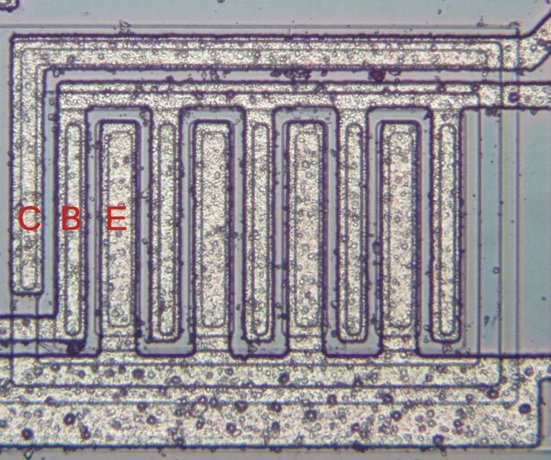
The output transistor (below) is much larger than the other transistors and has a different structure in order to support the chip's high-current output. It has multiple interlocking "fingers" for the emitter and base, surrounded by the large collector.

A large, high-current NPN output transistor in the LM185 chip. The collector (C), base (B) and emitter (E) are labeled.

A large, high-current NPN output transistor in the LM185 chip. The collector (C), base (B) and emitter (E) are labeled.

PNP transistors

You might expect PNP transistors to be similar to NPN transistors, just swapping the roles of N and P silicon. But for a variety of reasons, PNP transistors have an entirely different construction. They consist of a small circular emitter (P), surrounded by a ring-shaped base (N), which is surrounded by the collector (P). This forms a P-N-P sandwich horizontally (laterally), unlike the vertical structure of the NPN transistors.

The diagram below shows one of the PNP transistors in the LM185, along with a cross-section showing the silicon structure. Note that although the metal contact for the base is on the edge of the transistor, it is electrically connected through the N and N+ regions to its active ring in between the collector and emitter.

A PNP transistor in the LM185 chip. Connections for the collector (C), emitter (E) and base (B) are labeled, along with N and P doped silicon. The base forms a ring around the emitter, and the collector forms a ring around the base.

A PNP transistor in the LM185 chip. Connections for the collector (C), emitter (E) and base (B) are labeled, along with N and P doped silicon. The base forms a ring around the emitter, and the collector forms a ring around the base.

Resistors

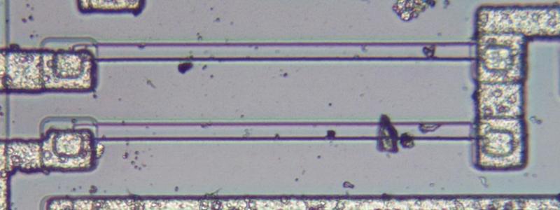
Resistors are a key component of analog chips. Unfortunately, resistors in ICs are large and inaccurate; the resistances can vary by 50% from chip to chip. Thus, analog ICs are designed so only the ratio of resistors matters, not the absolute values, since the ratios remain nearly constant. The photo below shows two paralleled resistors. Other resistors have a zig-zag shape to fit a longer resistor into the available space.

A resistor inside the LM185 chip. The resistor is a strip of P silicon between two metal contacts.

A resistor inside the LM185 chip. The resistor is a strip of P silicon between two metal contacts.

Capacitors

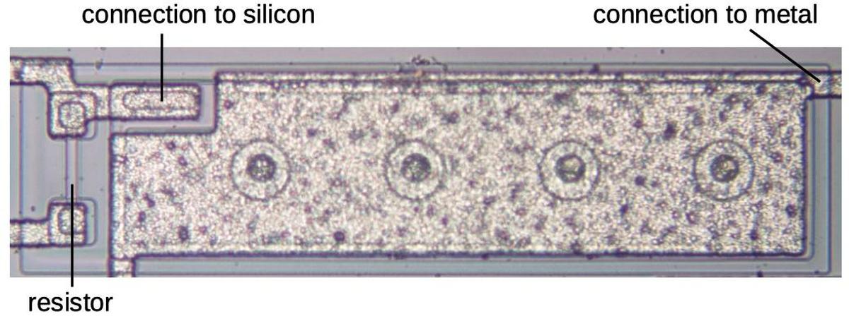
A capacitor consists of a metal plate on top of silicon, separated by a thin oxide layer that acts as a dielectric. Capacitors are fairly large on integrated circuits; they are the most visible components on this die. The capacitor below contains multiple circular patterns. These may be doped silicon regions, where the junction between two regions provides additional capacitance.

A capacitor on the die.

A capacitor on the die.

Fuses

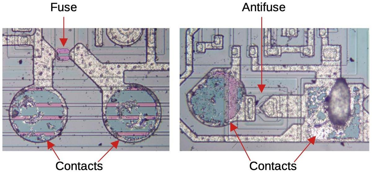
Fuses allow the circuitry of the chip to be changed after manufacturing. The LM185 uses fuses for two reasons. First, fuses can add or remove resistance, allowing the circuit to be tuned for higher performance. Second, a fuse changes the feedback circuitry between the LM185-1.2-N and LM185-2.5-N variants. (The LM185-ADJ version requires more changes than are supported by fuses, so it needs some changes to the metal layer. For instance, it has three pads connected instead of two.)

A fuse has two metal pads attached. Before the chip is packaged, probes can contact the pads and apply a high current to blow the fuse. The first type of fuse is implemented with a tiny strip of metal that is vaporized to break the circuit, just like a large-scale fuse. The second type of fuse is an "antifuse", which has the opposite behavior: it does not conduct until a high current is applied, at which point it becomes conductive. The antifuse can be built from a Zener diode, and the process of shorting it out is called a "Zener zap". The high current forms metal spikes through the junction, causing it to permanently conduct. The diagram below shows a fuse and an antifuse as they appear on the die.

A fuse and an antifuse on the die (I think). The contacts originally had more metal, but I used acid to clean gunk off the die and it dissolved some of the metal.

A fuse and an antifuse on the die (I think). The contacts originally had more metal, but I used acid to clean gunk off the die and it dissolved some of the metal.

IC circuit: The current mirror

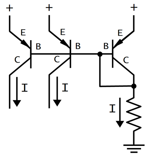
There are some subcircuits that are very common in analog ICs, but may seem mysterious at first. The current mirror is one of these. The idea is you start with one known current and then you can "clone" multiple copies of the current with a simple transistor circuit, the current mirror.

The following circuit shows how a current mirror is implemented with three identical transistors.2 A reference current passes through the transistor on the right. (In this case, the current is set by the resistor.) Since all the transistors have the same emitter voltage and base voltage, they source the same current, so the currents on the left match the reference current.

Current mirror circuit. The currents on the left copy the current on the right.

Current mirror circuit. The currents on the left copy the current on the right.

A common use of a current mirror is to replace resistors. As explained earlier, resistors inside ICs are both inconveniently large and inaccurate. It saves space to use a current mirror instead of multiple resistors whenever possible. Also, the currents produced by a current mirror are nearly identical, unlike the currents produced by two resistors.

Interactive chip explorer

To illustrate how the components form the chip, the die photo and schematic below are interactive. Click on a component in the die or schematic, and a brief explanation of the component will be displayed.

Click the die or schematic for details...

Because the three variants of the LM185 are slightly different, I had to combine three schematics to form the schematic above. Red components are only in the LM185-ADJ, green components are in the LM185-1.2-N, blue components are in the LM185-2.5-N, and cyan components are in the latter two chips. Note that the primary difference is the feedback circuit, but there are additional differences as well.

How a bandgap reference works

The main problem with producing a stable voltage from an IC is that the chip's parameters change as temperature changes. The bandgap voltage reference is commonly used to create a temperature-independent voltage reference.5 The trick is that it has one voltage that goes down with temperature and another than goes up with temperature. If you combine them correctly, you get a voltage that is stable with temperature.

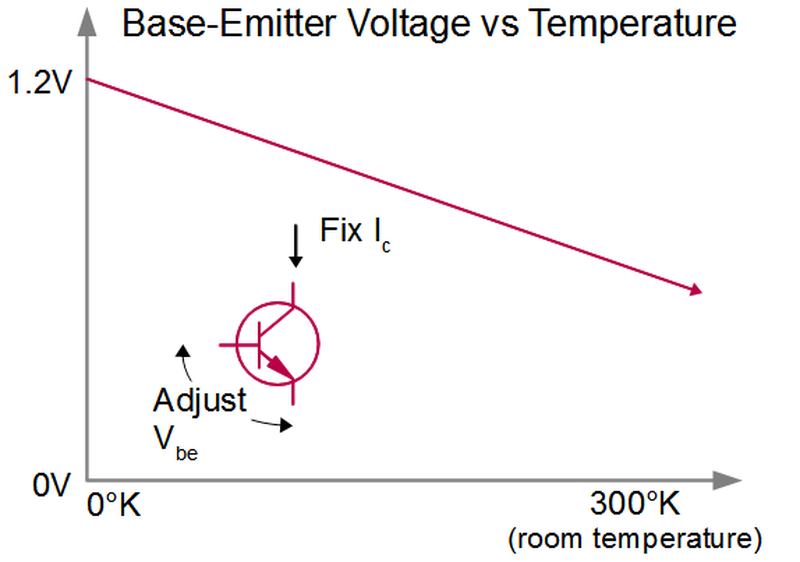
To create a voltage that goes down with temperature, you can put a constant current through the transistor and look at the voltage between the base and emitter, called Vbe. The graph below shows how this voltage drops as the temperature increases. At the left, the line hits the bandgap voltage of silicon, about 1.2 volts; this will be important later.

Vbe vs temperature for a transistor

Vbe vs temperature for a transistor

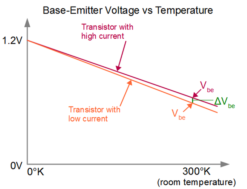
If you set up a second transistor this way but with a lower current3, you get the same effect but the voltage Vbe curve drops faster. This may not seem helpful since we need a voltage that goes up with temperature. But here's the trick: if you subtract the two Vbe voltages, the difference increases as temperature increases, since the lines get farther apart. The difference is called ΔVbe. The graph below shows the Vbe curves for two different transistors, and you can see how the difference ΔVbe between the curves increases with temperature, even though both curves decrease with temperature.

Voltages in a bandgap reference: Vbe for two transistors as temperature changes.

Voltages in a bandgap reference: Vbe for two transistors as temperature changes.

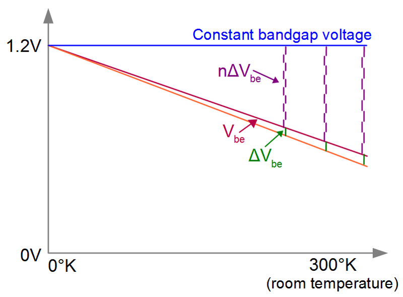
The final step to a bandgap reference is to combine Vbe and ΔVbe in the right ratio so the result is constant with temperature. It turns out that if the values sum to the bandgap voltage of silicon (approximately 1.2 volts), the drop in Vbe and the increase in ΔVbe cancel out. In the graph below, adding 10 copies of ΔVbe is the right ratio; the exact ratio depends on the particular transistors. The important thing to notice in the graph below is that as the temperature changes, Vbe+nΔVbe remains constant - the top of the blue ΔVbe line remains at the bandgap voltage.

By adding multiples of ΔVbe to Vbe, the bandgap voltage is reached regardless of temperature.

By adding multiples of ΔVbe to Vbe, the bandgap voltage is reached regardless of temperature.

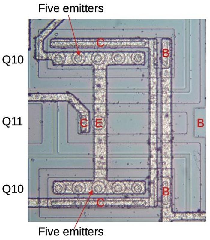
In the LM185, the key transistors are Q10 and Q11, where Q10 has 10 emitters in parallel, so each has 1/10 the current. Thus, if you feed the same current into both transistors, Q10 has a lower Vbe voltage than Q11 as described above. Note that Q10 is split in two: one half above Q11 and one half below Q11. This layout minimizes potential error due to a temperature gradient across the die. Half of Q10 will be hotter than Q11 and half will be cooler, so the difference will cancel out.

Transistors Q10 and Q11 are the key to the bandgap reference. Q10 has 10 emitters, so each has 1/10 the current as Q11.

Transistors Q10 and Q11 are the key to the bandgap reference. Q10 has 10 emitters, so each has 1/10 the current as Q11.

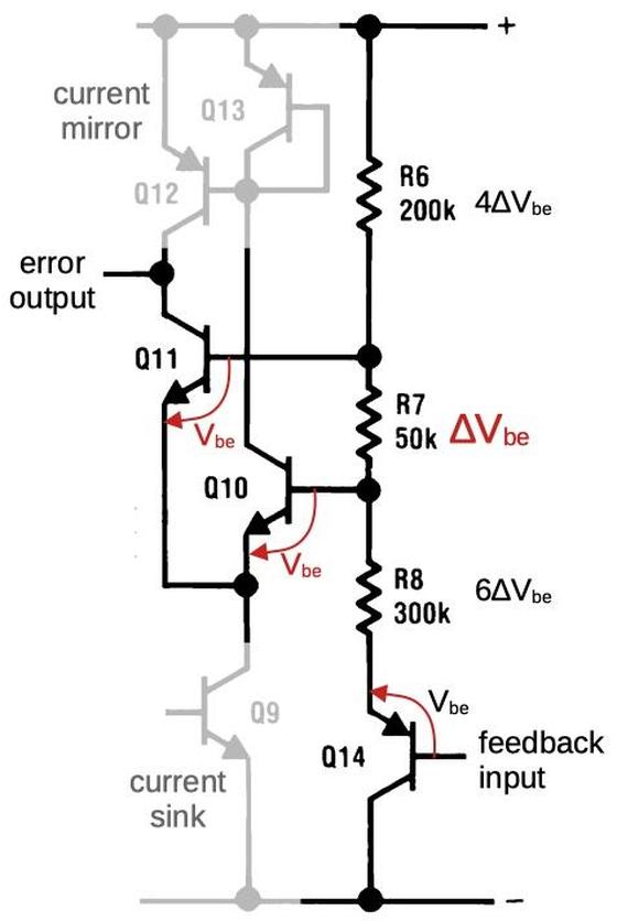
The diagram below shows how the bandgap reference is implemented in the LM185. Transistors Q10 and Q11 have different Vbe voltages due to their relative sizes. The difference in these voltages (ΔVbe) is developed across R7. Since the same current flows through R6, R7, and R8, the voltage across R6 will be 4ΔVbe and the voltage across R8 will be 6ΔVbe by Ohm's law. Thus, the combination of R6, R7, and R8 multiply ΔVbe by 11. Meanwhile, Q14 has its own Vbe.

The bandgap circuit in the LM185.

The bandgap circuit in the LM185.

Summing the voltages along the right gives Vbe + 11ΔVbe, which is designed to match the temperature-stabilized bandgap voltage of 1.2 volts. Thus, the circuit will be balanced4 if the voltage between the feedback input and V+ is 1.2 volts. If the voltage is not 1.2 volts, Q10 and Q11 will pass different amounts of current. Since the current mirror (Q12 and Q13) attempts to feed the same current into Q10 and Q11, any discrepancy will appear as current at the error output. This error current is amplified and controls the output transistor, adjusting the voltage until the feedback voltage is brought back into compliance. Thus, the circuit maintains the desired voltage, stabilized even if the temperature changes.

Conclusion

Well, that turned into a longer blog post than I was expecting. Although the LM185 doesn't contain many components by modern standards, it provides a stable, regulated voltage reference. It has some interesting features such as the use of fuses both to improve performance and to sell variant chips. It also illustrates the principle of the bandgap voltage regulator.

I announce my latest blog posts on Twitter, so follow me @kenshirriff. I also have an RSS feed. Thanks to Mitch Wright for supplying the chip.

Notes and references

  1. The LM185, LM285, and LM385 are the same chip, but with different temperature ranges. The LM185 is rated for the military temperature range: -55°C to 125°C. The LM285 is rated for the automotive temperature range: -40°C to 85°C. The LM385 is rated for the standard temperature range: 0°C to 70°C. I believe the chips are identical except for testing. For the purposes of this post, you can treat the three chips as identical. 

  2. For more information about current mirrors, check Wikipedia or chapter 3 of Designing Analog Chips

  3. When building a bandgap reference, what really matters for Vbe is the current density through the transistors - the current divided by the area of the emitter. Decreasing the current through the transistor decreases the current density. The second way to decrease current density is to use a larger transistor with a larger emitter. Often five or ten identical transistors in parallel will be combined to form this large transistor to ensure the large transistor and the small transistor are exactly matched. 

  4. One tricky thing about the bandgap circuit is that it is implemented "backward", taking the voltage as an input. The chip's block diagram6 shows that the reference generates 1.2 volts and this is compared to the input voltage. But in reality, the input voltage is fed into the bandgap circuit. If the input is 1.2 volts, the circuit is balanced. But if the input is too high or too low, the bandgap circuit will be unbalanced with more current through one transistor than the other. This "error" signal is amplified and used as feedback to adjust the input voltage until it matches 1.2 volts. In other words, there's no 1.2-volt reference inside the chip. Instead, the chip and its external input form a feedback loop that generates 1.2 volts. 

  5. I've written before about bandgap references, specifically the 7805 voltage regulator and the TL431

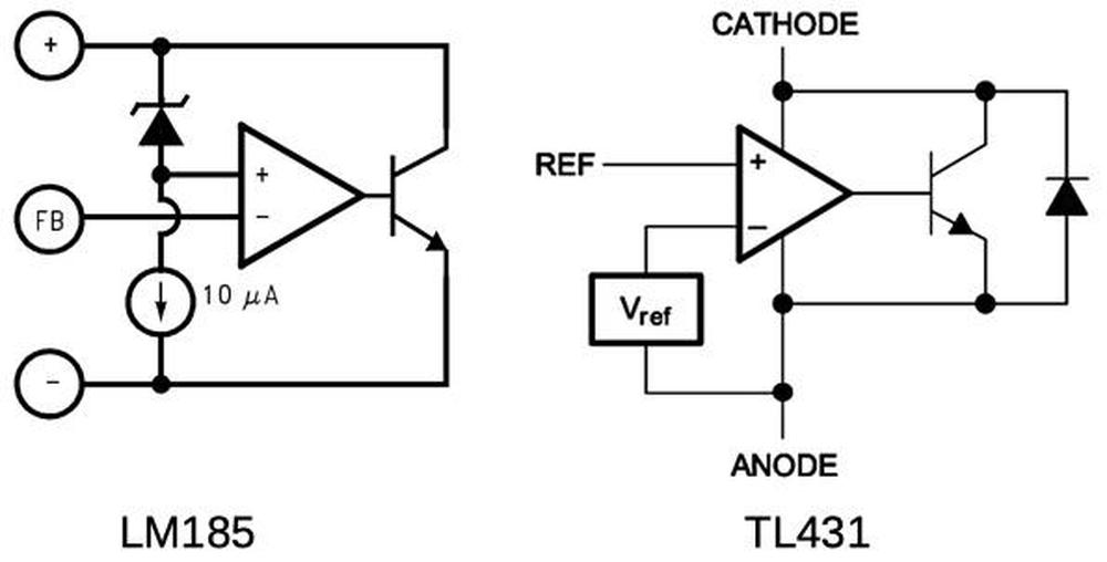
  6. The TL431 is a popular voltage reference, used in many power supplies. The main difference is that the LM185 regulates the voltage relative to the positive side, while the TL431 regulates the voltage relative to the negative side.

    Comparison of the LM185 and TL431 block diagrams, from the datasheets.

    Comparison of the LM185 and TL431 block diagrams, from the datasheets.


Reverse-engineering a mysterious Univac computer board

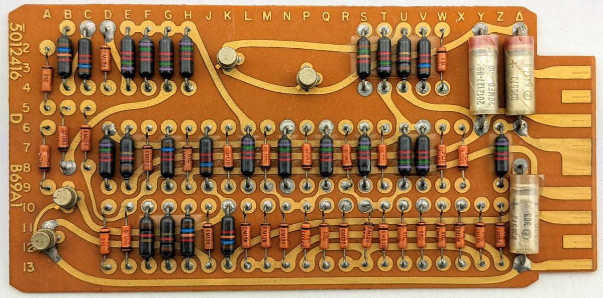
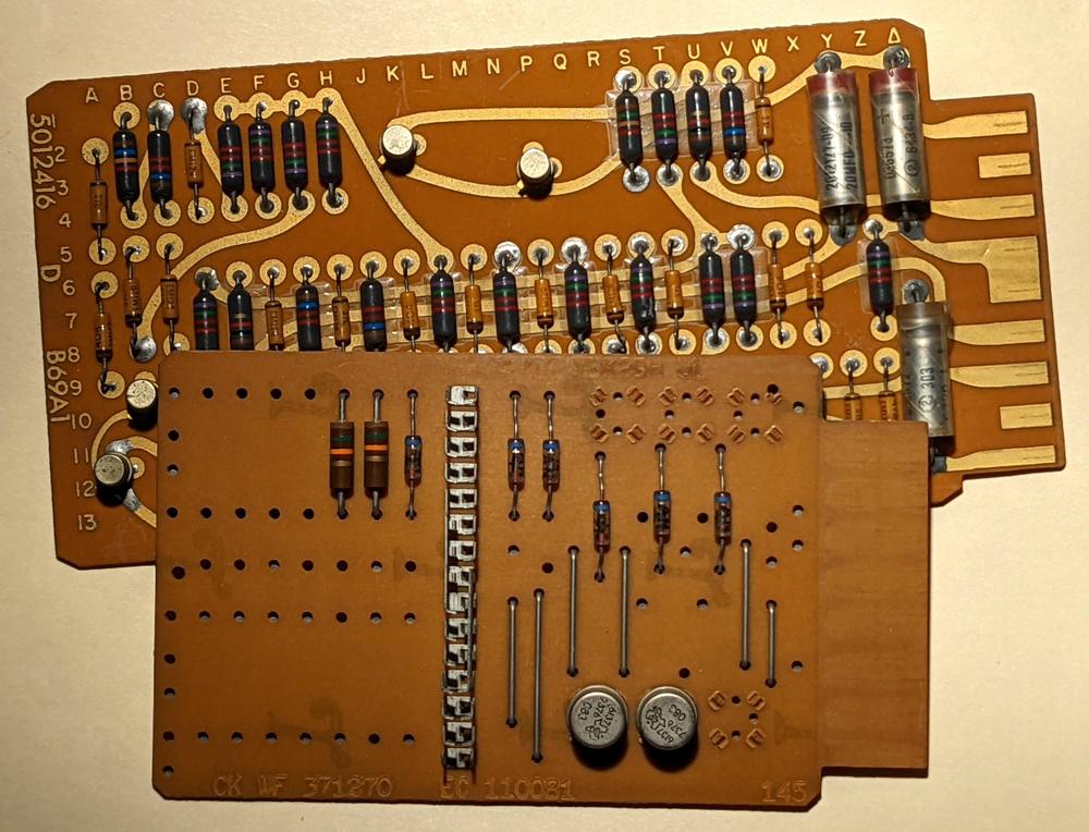
The IBM 1401 team at the Computer History Museum accumulates a lot of mystery components from donations and other sources. While going through a box, we came across the unusual circuit board below. At first, it looked like an IBM SMS (Standard Modular System) card, the building block of IBM's computers of the late 1950s and early 1960s.1 However, this board is larger, has double-sided wiring, the connector is different, and the labeling is different.2

The circuit board is about 15cm×7.3cm.

The circuit board is about 15cm×7.3cm.

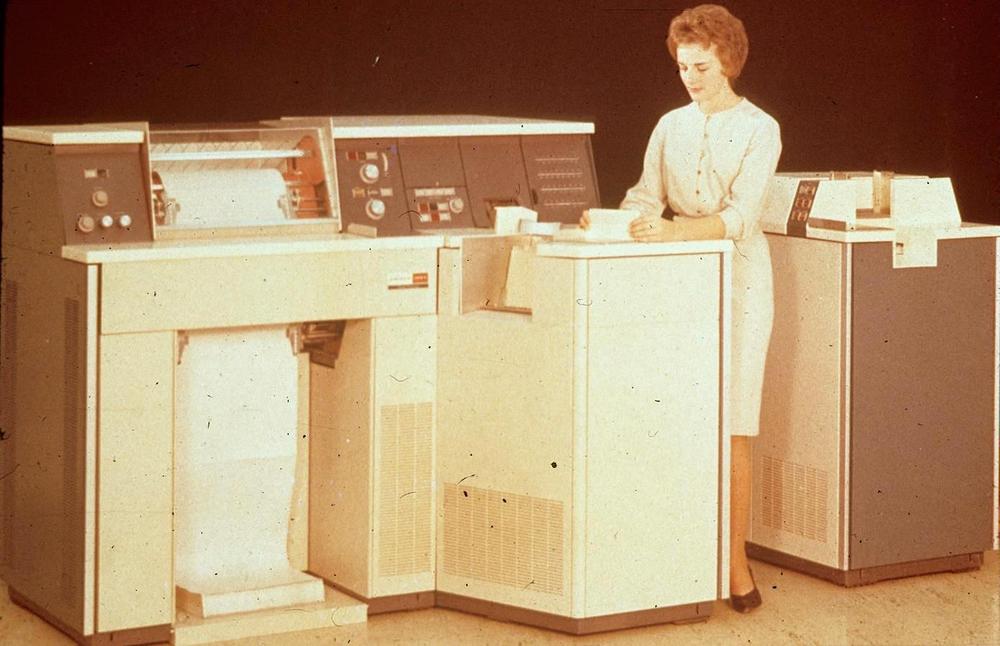
I asked around about the board and Robert Garner identified it as from the Univac 1004, a plugboard-controlled data processing system from 1963.4 The Univac 1004 was marketed as a "Card Processor" rather than a computer,3 designed for business applications that read punch cards and producing output, but still required calculation and logical decisions. Typical applications were payroll, inventory, billing, or accounting.

Photo of the Univac 1004. From bitsavers.

Photo of the Univac 1004. From bitsavers.

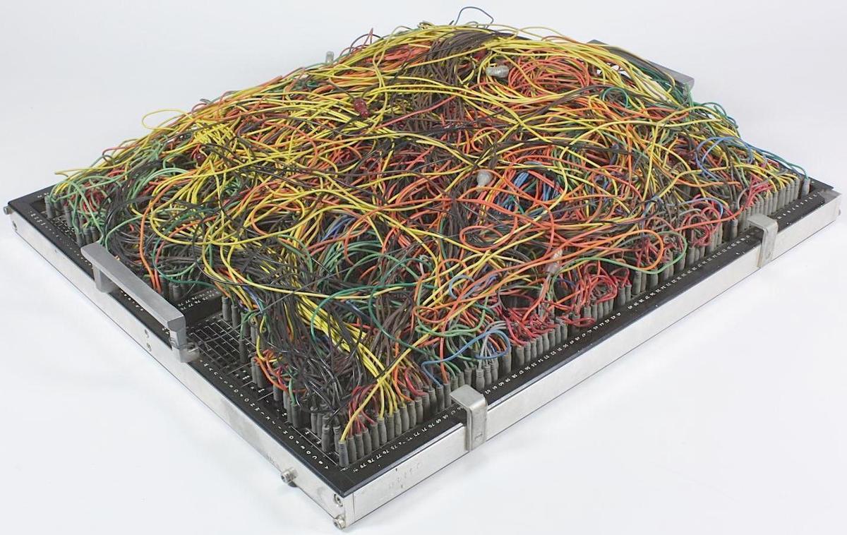
The most unusual feature of the Univac 1004 was that it was programmed by a plugboard (below) instead of a stored program. The system was programmed by plugging patch cords into a plugboard to indicate the desired action for each of the 31 program steps. While earlier electromechanical accounting machines used plugboards, they were pretty much obsolete by 1963, so I was a bit surprised to see plugboards still in use.

A plugboard for the Univac 1004. This board was used for payroll consolidation from 1965 to 1972. From Museums Victoria Collections, Copyright Museums Victoria / CC BY 4.0.

A plugboard for the Univac 1004. This board was used for payroll consolidation from 1965 to 1972. From Museums Victoria Collections, Copyright Museums Victoria / CC BY 4.0.

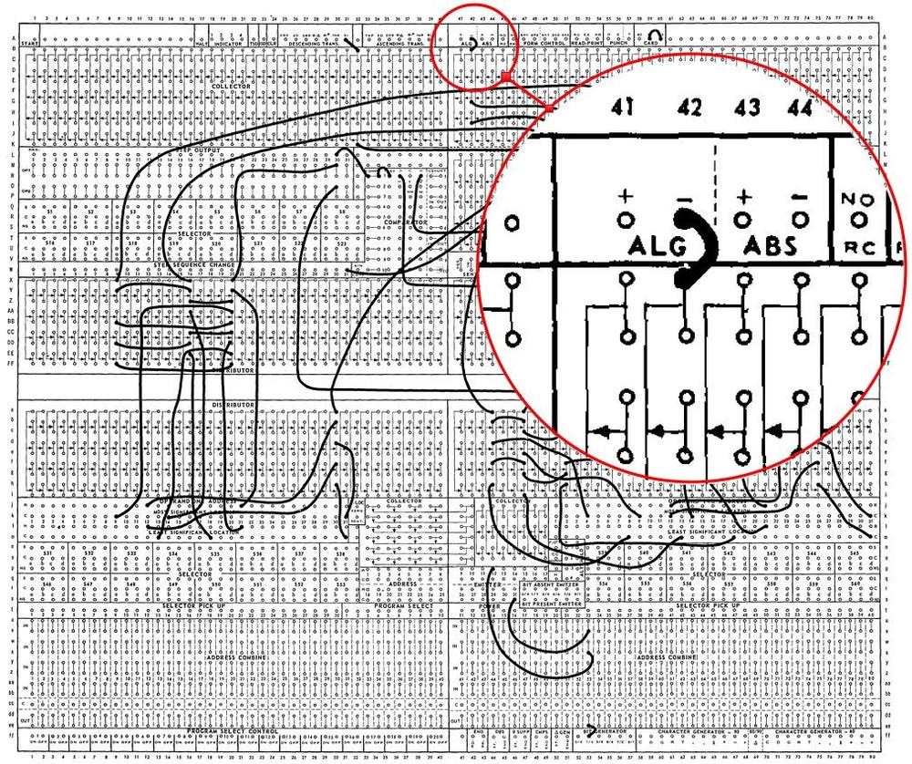
The computer's "program" consisted of 31 steps. The operations for each step were specified by plugging wires into the board. For instance, a data field could be moved from a punch card to memory, a value could be added or subtracted, or a line of output could be configured for the printer.5 The system even supported conditional branches. The diagram below shows the structure of the plugboard. The highlighted wire shows a subtraction operation, activated by the wire in the "algebraic minus" position.

Part of a program in the plugboard.  Click for a larger version. From the Reference Manual.

Part of a program in the plugboard. Click for a larger version. From the Reference Manual.

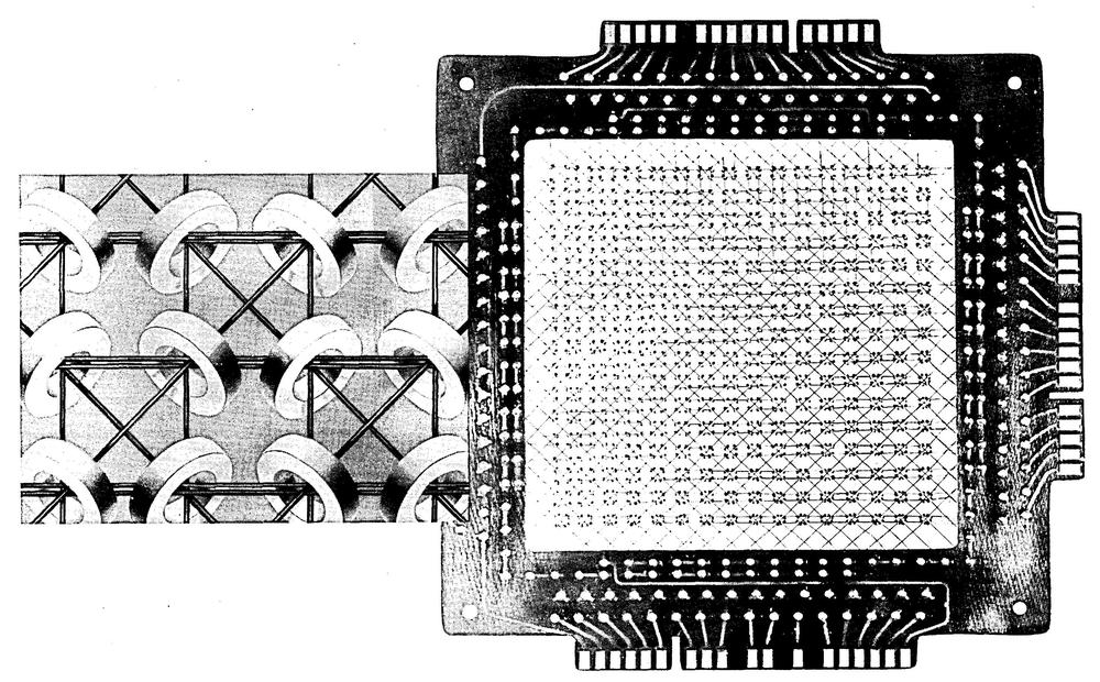
The computer had a small memory of 961 6-bit characters. Like most computers of the era, it used magnetic core memory, storing each bit by magnetizing a tiny ferrite ring. Note that since the computer was programmed through a wiring panel, none of the memory was used for program code.

A plane of magnetic core storage, from the Reference Manual.

A plane of magnetic core storage, from the Reference Manual.

While the Univac 1004 was primitive for its time compared to even a low-end business computer like the IBM 1401, it had a few advantages. First, it rented for $1900 a month, compared to $2500 a month for the IBM 1401 (about $18,000 vs $23,000 a month in current dollars). Second, the Univac computer was compact (by 1960s standards), weighing 2500 pounds. Finally, many customers found plugboard programming easier than programming with code, both because they were more familiar with it and because it is visual and direct.

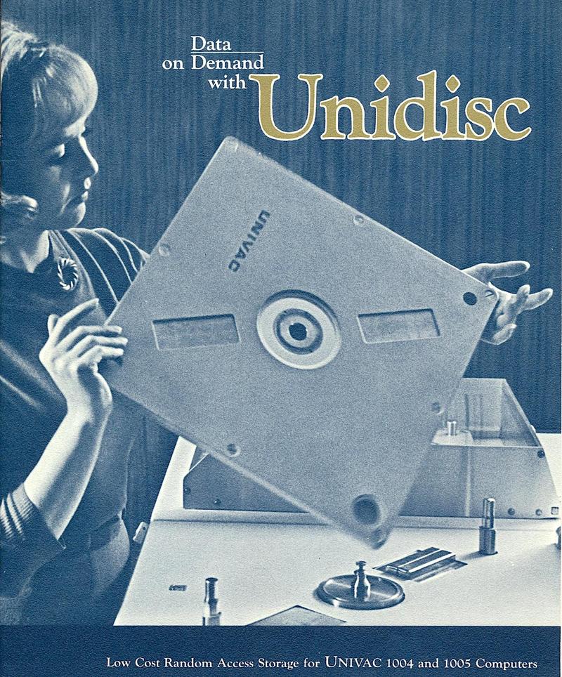
The Univac 1004 could be extended with peripherals such as tape drives, a card punch, or disk storage. The photo below shows the Unidisc cartridge, which held one million characters. Although it looks like an absurdly-large floppy disk, it was a removable hard disk.

The Unidisc cartridge is 15¾ inches square and ⅝-inch thick. (source).

The Unidisc cartridge is 15¾ inches square and ⅝-inch thick. (source).

Reverse-engineering the board

The function of the board wasn't immediately obvious and we had various theories of what it might do. To find out, I reverse-engineered the board by tracing out the circuitry.6 The board has 32 diodes, which seems like a lot, as well as resistors, transistors, and capacitors. The transistors are not silicon transistors, but germanium PNP transistors.

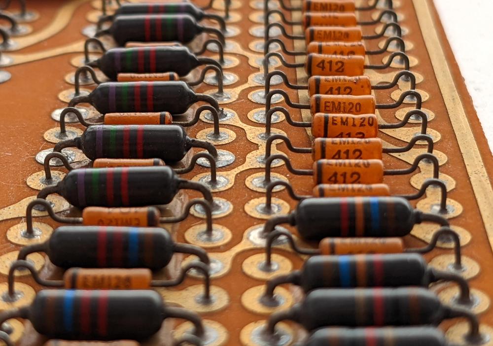
A closeup of the circuit board showing resistors and diodes.

A closeup of the circuit board showing resistors and diodes.

The board turned out to be a logic board implemented with AND-OR-INVERT logic.7 That is, various inputs are ANDed together, the AND results are then ORed together, and finally the result is inverted. The board is implemented with diode-transistor logic. One layer of diodes implements the AND gates and the second layer of diodes implements the OR gates. Finally, a transistor amplifies the result, inverting it in the process. Diode-transistor logic (DTL) performed better than earlier resistor-transistor logic (RTL), but was soon replaced by transistor-transistor logic.

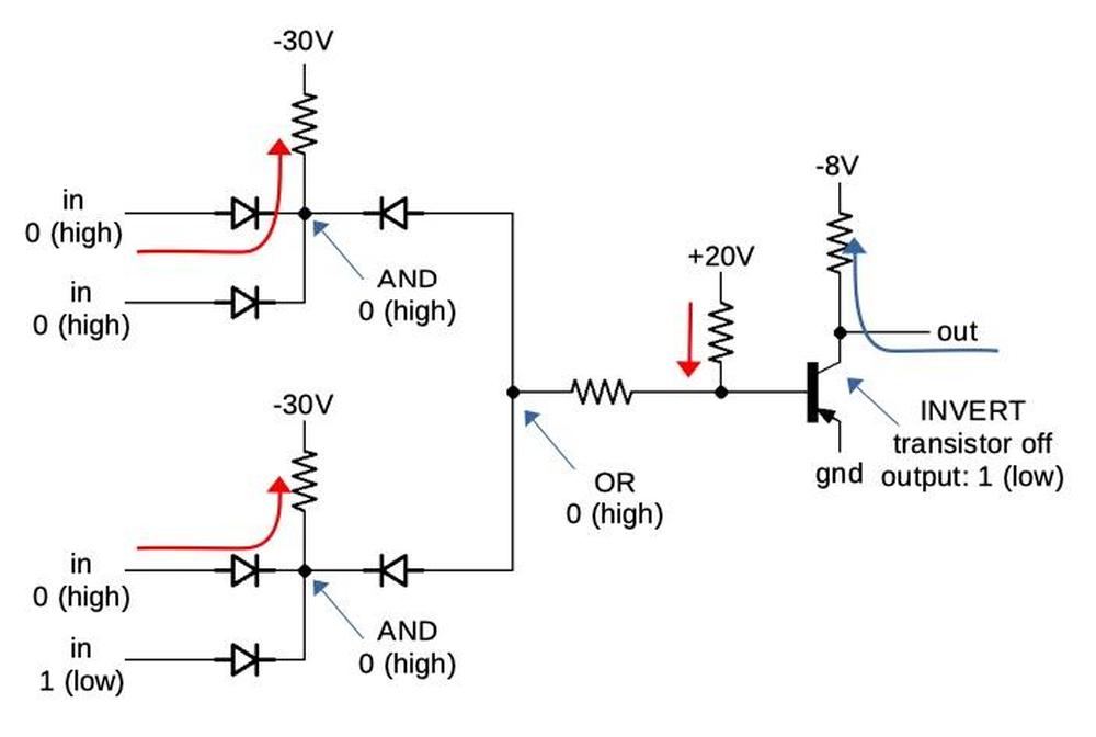
The diagram below explains how the AND-OR-INVERT logic was implemented. This circuit has four inputs: two AND gates that are then ORed together and inverted. (It's a bit confusing because the circuit uses active-low logic, so the voltage levels are all inverted.) If the AND gates all have a 0 (high) input, a diode in the first stage will conduct and pull the AND node high. This blocks the diodes in the second stage (which have the opposite orientation), so the OR node is also high. In the INVERT stage, the +20V resistor will pull the transistor's base high, which turns it off (since it is PNP). Finally, the -8V resistor will pull the output low (i.e. 1), providing the desired AND-OR-INVERT logic.

The AND-OR-INVERT logic producing a 1 output.

The AND-OR-INVERT logic producing a 1 output.

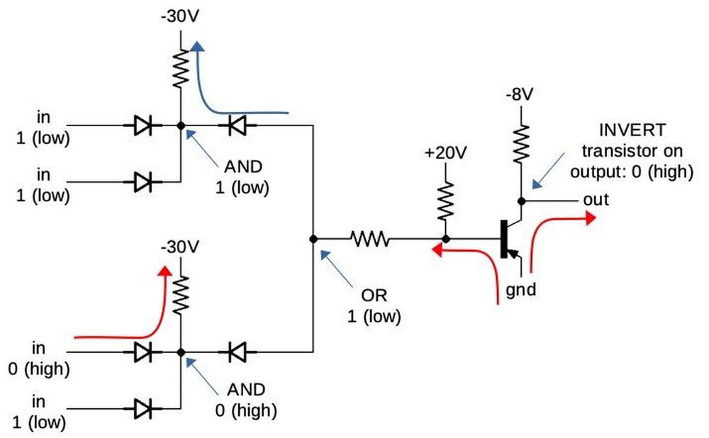
The diagram below shows that if the first AND gate's inputs are 1 (low), the first diodes are blocked, so the -30V resistor pulls the AND node low (1). Now the second-stage diode conducts, pulling the OR node low (1). This allows base current to flow through the PNP transistor, turning it on. This pulls the output high (0). (Note that ground is a high output compared to the low output of -8V.) The gates on the board have more inputs, but use the same principle.

The AND-OR-INVERT logic producing a 0 output.

The AND-OR-INVERT logic producing a 0 output.

After tracing out the board's logic, I recognized that it implemented a full adder.8 That is, it adds two input bits along with a carry-in, producing a sum bit and a carry-out. By connecting four full-adders in series, a 4-bit value can be added, allowing one decimal digit to be added. Thus, the computer probably has four one-bit adder boards similar to this, along with circuitry to convert the output from binary to binary-coded decimal.10

The board has a few additional circuits along with the full adder circuit. It includes an inverter circuit. The board also has 4 inputs that are ANDed, subject to the carry value. Finally, the board also has a disable input that blocks the outputs.9 Without knowing more about the circuitry, I can't determine the role of these circuits.

Conclusion

The mystery circuit board turned out to be from the Univac 1004. Although this computer was produced in the 1960s, its technology occupies an interesting location between the electro-mechanical accounting machines of the 1940s and the electronic business computers of the late 1950s. The Univac computer used transistors and core memory, but it kept the earlier plugboard programming of the accounting machines, rather than moving to stored-program computing (introduced in 1948). Even though the Univac 1004 was technologically backward for 1963, businesses flocked to it, making it the second-most popular computer at the time with 3400 installations.4

This shows that progress isn't as linear as you might expect; "obsolete" technologies can continue to thrive long after the introduction of "superior" alternatives such as stored-program computing. Instead, new systems can still be developed with supposedly-obsolete technologies, depending on the tradeoffs involved.

I announce my latest blog posts on Twitter, so follow me @kenshirriff. I also have an RSS feed.

Notes and references

  1. The Computer History Museum links to a similar board

  2. The photo below compares the Univac board to a smaller IBM SMS board.

    Comparison with an IBM SMS card.

    Comparison with an IBM SMS card.


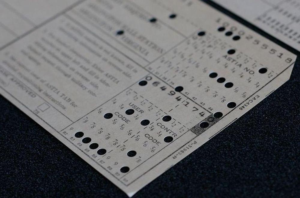
  3. The Univac 1004 computer came in two versions. The "80" read standard IBM 80-column punch cards. The "90" read Univac's 90-column cards (details), which held 90 characters per card instead of 80. The 90-column card was introduced in 1930 by Remington Rand. It had round holes instead of IBM's rectangular holes. The card stored two characters per column by using a denser, binary code. Despite the superior capacity of the 90-column card, IBM's 80-column cards dominated the market. (Even IBM couldn't displace the 80-column card, although they tried with the 96-column card that they introduced in 1969.)

    A 90-column punch card. From Marcin Wichary,  (CC BY 2.0).

    A 90-column punch card. From Marcin Wichary, (CC BY 2.0).


  4. Robert Garner discusses the Univac 1004 briefly in his article on Early Popular Computers. More information is in the 1964 BRL report as well as on Bitsavers. A related board from the Univac 1040/1050 is described here

  5. The plugboard supported conditionals and looping, so I think the system was Turing-complete, although you couldn't do a lot in 31 programming steps. You could implement multiplication or division with a short shift and add (or subtract) loop. 

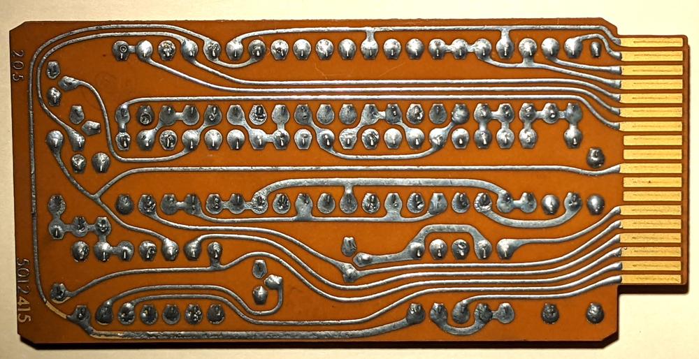
  6. To reverse-engineer the board, I took photos of both sides, flipped the image of the back in GIMP so the two sides were aligned visually, arranged the components on a schematic in EAGLE, and connected the components to match the circuit board. Then I moved the components around until the layout made sense.

    The underside of the circuit board.

    The underside of the circuit board.

    The back of the circuit board is shown above. Note that the edge connectors are completely different on the two sides of the board.


  7. AND-OR-INVERT logic was also used in the IBM System/360 computers, although it was built from hybrid SLT modules instead of discrete components. 

  8. I suspected the board was an adder when I saw that it had three inputs and was combining them symmetrically. The full adder is implemented in AND-OR-INVERT logic as follows. If the two bits are A and B and the carry-in is CIN, then a carry-out (COUT) is generated if at least two input bits are set. This is computed by the AND-OR logic "(A and B) or (A and CIN) or (B and CIN)". The sum bit is set if there is a single 1 input or three 1 inputs. The sum bit was computed by "(A and not COUT) or (B and not COUT) or (CIN and not COUT) or (A and B and CIN)" As a result of the AND-OR-INVERT circuit, the output is inverted. The inverter circuit on the board was probably used to un-invert it. 

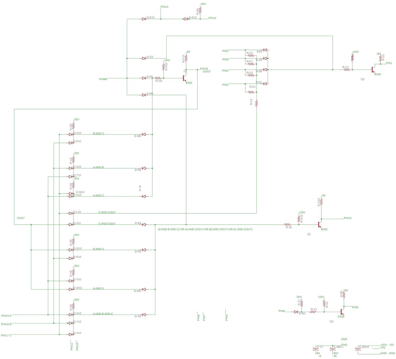
  9. The full reverse-engineered schematic is below.

    Reverse-engineered schematic of the board. Click for a larger version.

    Reverse-engineered schematic of the board. Click for a larger version.


  10. The computer uses excess-three encoding for digits, adding 3 to the value before converting to binary. For example, 6 is represented as binary 1001. The advantage of this encoding is that flipping the bits yields the 9's-complement decimal value, simplifying subtraction. For example, flipping the bits of 6 yields binary 0110, which is 3 in excess-3 notation. Excess-3 representation also handles carries correctly; if you add two numbers that sum to 10, the excess-3 values will sum to 16, causing a binary carry. To convert the sum to excess-3, The value 3 must be added (if a carry) or subtracted (if no carry).

    To see how addition works with excess-3, 2 + 4 in excess-3 is binary 0101 + 0111 = 1100. Subtracting 3 yields 1001, which is 6 in excess-3. But 2 + 9 is binary 0101 + 1100 = 10001, generating a carry out of the 4 bit value. Adding 3 yields 0100, which is 1 in excess-3. Considering the carry-out, this is the desired result of 11. 

Inside the Apple-1's shift-register memory

Apple's first product was the Apple-1 computer, introduced exactly 46 years ago, on April 11, 1976. This early microcomputer used an unusual type of storage for its display: shift register memory. Instead of storing data in RAM (random-access memory), it was stored in a 1024-position shift register. You put a bit into the shift register and 1024 clock cycles later, the bit pops out the other end. In the early days of random-access memory chips, shift-register memory was cheaper so many systems used it.1 The downside, of course, is that you had to use bits as they became available, rather than access arbitrary memory locations.2

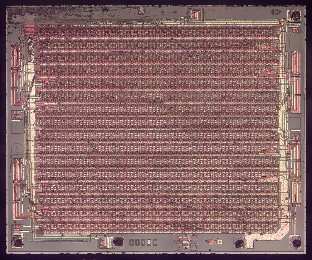
Die of the Signetics 2504 shift register chip. Click this image (or any other) for a larger version.

Die of the Signetics 2504 shift register chip. Click this image (or any other) for a larger version.

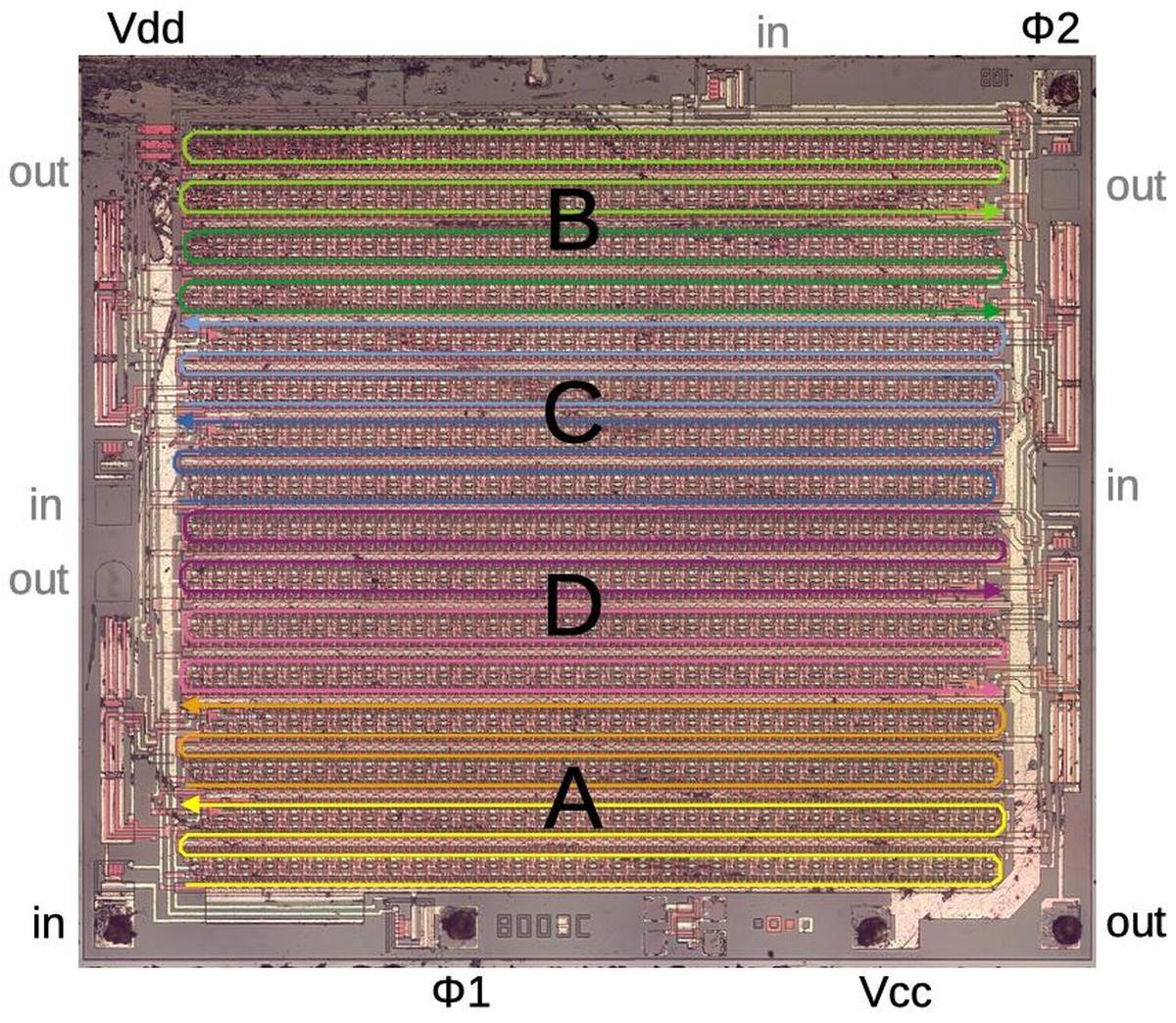
The photo above shows the chip under the microscope. The underlying silicon is grayish, with white metal wiring on top. The thickest metal wiring provides power to the chip. The chip also has wiring and transistors constructed from a type of silicon called polysilicon; the polysilicon appears red in the photo. Most of the die is occupied by the shift register, arranged in rows that snake back and forth. The squares around the edge of the die are bond pads, where bond wires connect the die to the chip's external pins.3

The Apple-1's display

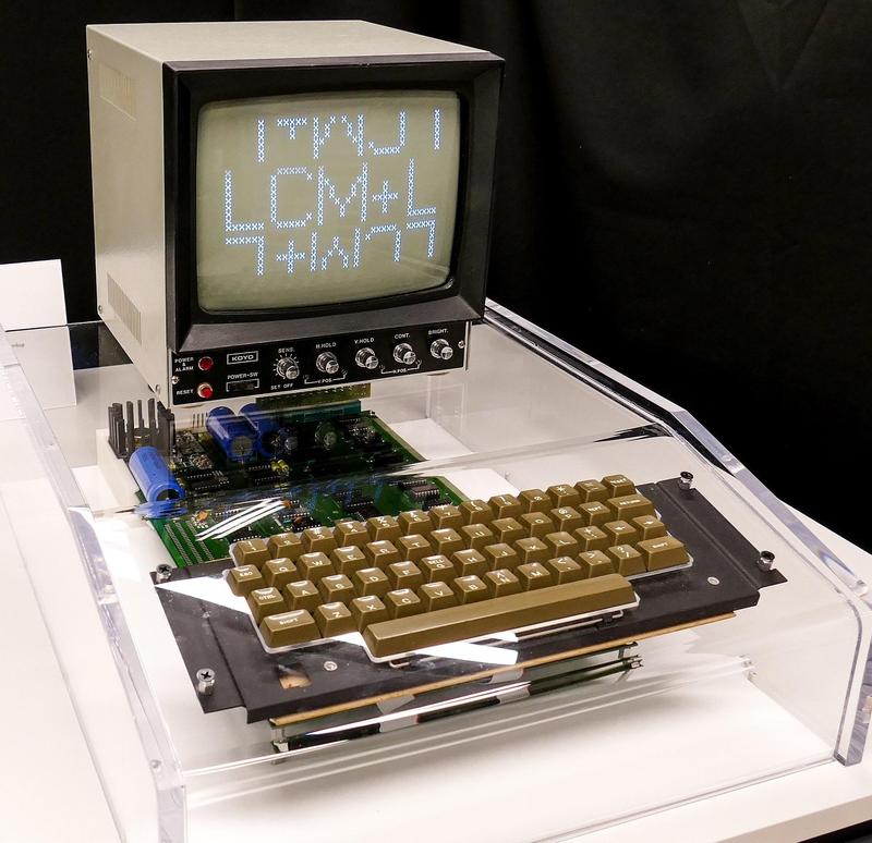
The Apple-1 displayed 24 lines of forty characters on a television monitor. Like most computers at the time, the Apple-1 stored characters rather than pixels to reduce memory requirements. A character-generation ROM converted each character into a 5×7 matrix of pixels as it was displayed. To reduce memory even more, the display didn't store full bytes, but 6-bit characters, supporting upper-case letters, numbers, and some symbols.

The Apple-1 computer was sold as a circuit board. The user had to supply a keyboard, power supply, display, and case. Photo by Cynde Moya, CC BY-SA 4.0.

The Apple-1 computer was sold as a circuit board. The user had to supply a keyboard, power supply, display, and case. Photo by Cynde Moya, CC BY-SA 4.0.

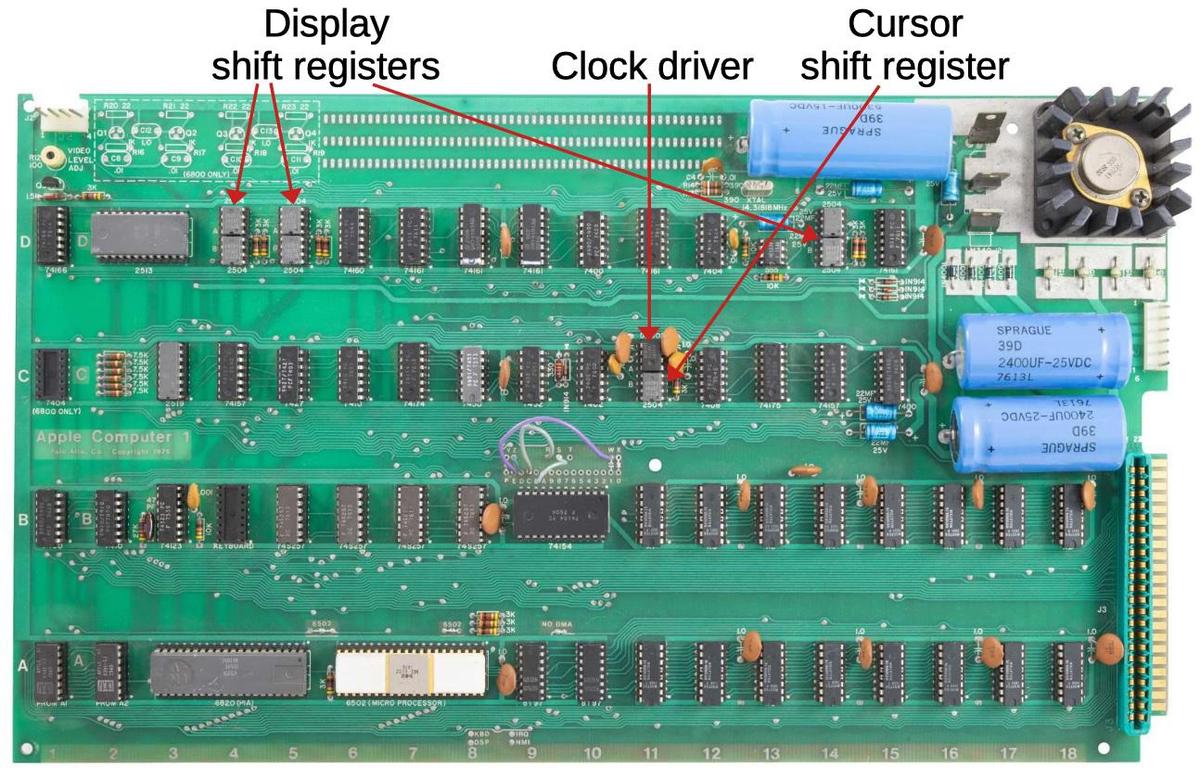
The six-bit display characters were held in six 1024-bit shift registers. A seventh shift register tracked the cursor position.4 The diagram below shows the shift registers and the clock driver on the Apple-1 circuit board. These chips are in 8-pin packages, so two chips fit into the space of a regular TTL chip.5

Apple-1 circuit board, showing the 1024-bit shift register chips and the clock driver chip.
Original image from
Achim Baqué, CC BY-SA 4.0.

Apple-1 circuit board, showing the 1024-bit shift register chips and the clock driver chip. Original image from Achim Baqué, CC BY-SA 4.0.

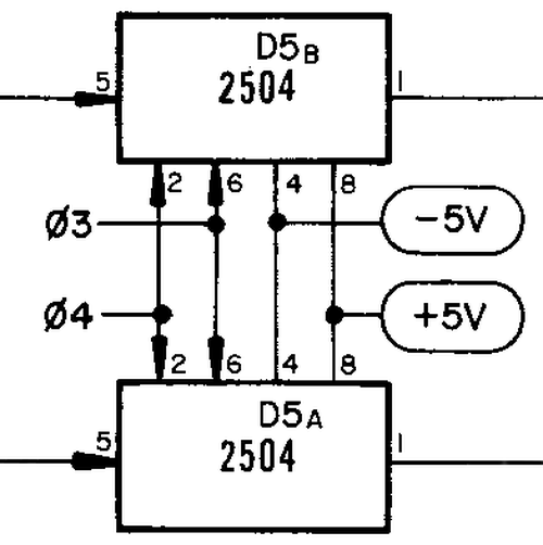
The image below shows how the 2504 shift register chips are represented on the Apple-1 schematic. The chips use just 6 pins. Each chip has a single connection for bits coming in and a connection for the bits coming out. The remaining pins provide the two clock signals and the ±5 volt power supplies. Unlike RAM chips, these chips do not take an address.

Detail of the Apple-1 schematic showing two of the shift register chips.

Detail of the Apple-1 schematic showing two of the shift register chips.

PMOS integrated circuits

This shift register chip was created around 1970, an interesting time in the development of MOS integrated circuits. Early integrated circuits used a type of transistor known as bipolar. However, the metal-oxide-semiconductor (MOS) transistor had the potential to make cheaper, high-density integrated circuits. The first commercial MOS integrated circuit was a 20-bit shift register, created in 1964 by a company called General Microelectronics.

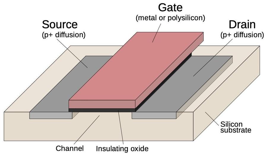
The diagram below shows the structure of a MOS transistor. At the bottom is the silicon, which is doped with impurities to form p-type silicon. The two conductive p-type regions are called the transistor's source and drain. The channel acts as a switch between the source and drain, turned on by voltage in the metal gate above. A thin insulating oxide layer separates the metal gate from the underlying silicon. These three layers—metal, oxide, semiconductor— give the MOS transistor its name. In the late 1960s, chips started to use gates made of polysilicon, a special type of silicon that produced better transistors than metal gates. This is the technology used by the 2504 shift register: the "P-MOS silicon gate process".

Structure of a P-type MOSFET.

Structure of a P-type MOSFET.

By the mid-1970s, however, integrated circuits changed in two more ways. First, P-MOS transistors were replaced by N-MOS transistors, which had better performance. Second, the introduction of ion implantation machines allowed transistor characteristics to be adjusted, with "depletion-mode" transistors8 leading to faster, lower-power circuitry. These changes ushered in the age of popular microprocessors such as the Zilog Z80, MOS Technology 6502, and Intel 8085. These had much better performance than earlier PMOS processors such as the Intel 8008.7 The 6502, of course, was the processor in the Apple-1 (and Apple II).

The shift register

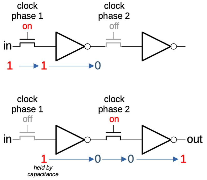
Next, I'll look at the details of how the shift register was constructed. The idea of a shift register is that bits are passed from stage to stage, controlled by clock pulses. With 1024 stages, the shift register can hold 1024 bits. Each shift register stage uses two transistors and two inverters as shown below. During the first clock phase, the first transistor turns on, allowing the input bit to pass through it and the first inverter. During the second clock phase, the second transistor turns on, allowing the inverted value to pass through it and the second inverter, producing the output. Thus, a bit takes two clock phases to move through the shift register stage.

In the first clock phase, the input passes through the first transistor. In the second clock phase, the input is held by the gate capacitance and passes to the output.

In the first clock phase, the input passes through the first transistor. In the second clock phase, the input is held by the gate capacitance and passes to the output.

This circuit is a dynamic shift register, which works due to the circuit's capacitance. When the first transistor turns off, the value remains at the input to the first inverter, held by the capacitance of the circuit. (And likewise for the second transistor.) Because the gate of a MOSFET uses almost no current, the bit value will remain for a couple of milliseconds or so before it drains away. (This is the same principle used by DRAM, holding bits through capacitance.) As long as the clock keeps going, the bit gets refreshed by each stage.

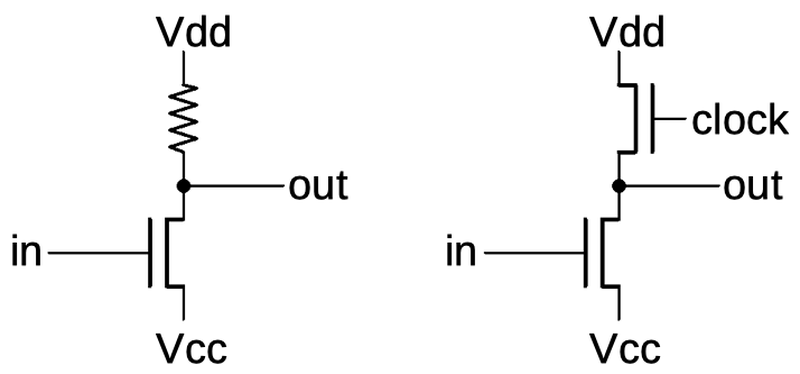
Each inverter is implemented using two MOS transistors. The concept is shown on the left, below. A high input turns on the transistor, which pulls the output low. A low input turns off the transistor allowing the pull-up resistor to pull the output high. Thus, the circuit inverts its input.

Conceptually, the inverter uses the circuit on the left. The implementation uses the circuit on the right.

Conceptually, the inverter uses the circuit on the left. The implementation uses the circuit on the right.

The circuit is actually implemented with a transistor in place of the resistor, as shown on the right, because transistors are more compact than resistors. A high input to the upper transistor turns it on, causing the pull-up current to flow. In a standard inverter, the transistor would be connected to be always on.9 However, the output of the inverter is only used during one clock phase. To reduce power consumption, the transistor is wired to the clock so it only acts as a pull-up when needed.

A shift-register stage on the die

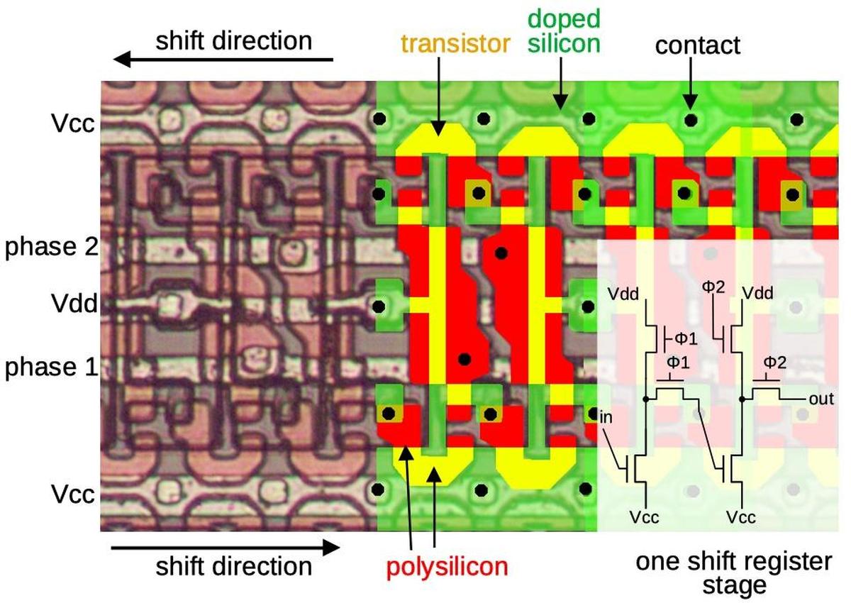
The diagram below shows how shift-register stages are physically constructed on the die. The first part of the image shows how the circuitry appears under the microscope, a complicated jumble of silicon, polysilicon, and metal circuitry. In the middle, I've highlighted the doped silicon in green and the polysilicon in red. A transistor gate (yellow) is formed where polysilicon crosses silicon, with the source and drain on either side. (The horizontal metal wiring should be clear without highlighting.) Note the complex, optimized shapes of the polysilicon and the transistors. Finally, a black dot indicates a contact that connects two layers. In the bottom half of the image, bits are shifted to the right, while in the top half, bits are shifted to the left.

One stage of the shift register.

One stage of the shift register.

In the lower right, one stage of the shift register is represented by a schematic on top of the underlying circuitry. The stage is implemented with six transistors as described earlier. Note that the pull-up transistors to Vdd are long and skinny, reducing their current. The inverter transistors to Vcc, on the other hand, are wide, so they provide a lot of current. The circuitry in the top half of the image is the same, but rotated 180°. Note that the two rows of shift registers share the clock phase lines and Vdd, making the layout more efficient.6

Topology of the chip

You might expect the chip to consist of 1024 shift-register stages arranged into a chain. However, the chip had an unusual topology that allowed it to operate at double speed: one bit per clock phase instead of one bit per complete clock cycle. It accomplished this with a simple trick: it was really two 512-bit shift registers operating in parallel. The first operated on clock phase 1, phase 2, phase 1, ..., while the second was the opposite: phase 2, phase 1, phase 2, ... The result was that one half would produce bits in phase 1, while the other would produce bits in phase 2. The output circuit merged these together into a single output stream. From the outside, it looked like a 1024-bit shift register that operated twice as fast.

Another complication is that Signetics produced three 1024-bit shift register chips from the same silicon layout: the 2502 (organized as four 256-bit shift registers), the 2503 (512×2), and the Apple-1's 2504 (1024×1). The different chips were created by changing the metal wiring of the chip during manufacturing, which was much easier than building completely different chips. To support this, the shift register was broken into eight 128-bit segments, shown below. In the 1024×1 chip, two chains of four 128-bit segments ran in parallel (on opposite clock phases) to produce a 1024-bit shift register. The first chain used the light-colored segments A, B, C, D, while the second chain used the dark-colored segments. The segments are connected by the metal wiring along the side of the die. The chip's pads around the edges are labeled; the grayed-out ones are not used in this chip. The large block of circuitry above the output pin combines the two chains into one output.

The chip consists of 8 shift-register chains, each 128 bits long. They are connected in different ways to form different shift register chips.

The chip consists of 8 shift-register chains, each 128 bits long. They are connected in different ways to form different shift register chips.

The other variants of the chip wire the shift-register segments differently and use additional input and output pins. The 512×2 2503 chip used four chains of 256 bits along with two input and output circuits. The 2502B chip used all eight 128-bit chains in parallel to form a 256×4 shift register, with four input and output circuits.10

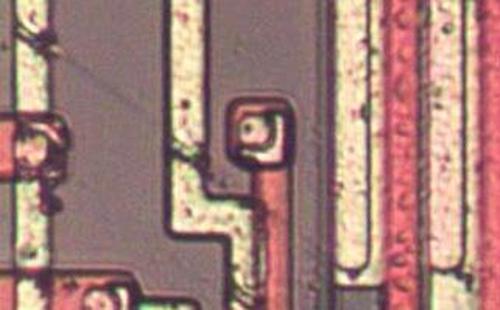
The image below shows one of the unconnected outputs: the red polysilicon wire isn't connected at one end. With a small change to the metal layer, the metal wiring between two segments can be broken and the segment wired to this output instead. The other changes between chip versions are similar.

The polysilicon wire in the middle is disconnected.

The polysilicon wire in the middle is disconnected.

The clock driver

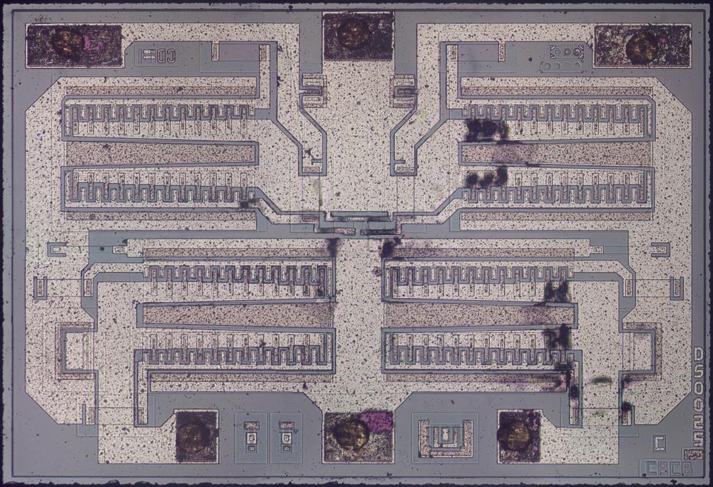
I'll wrap up with a brief mention of the clock driver chip that drives the shift registers. Shift-register memory chips required clock pulses with high current and unusual voltages due to the PMOS circuitry: from +5 volts to -11 volts. These pulses were provided by a special chip, the DS0025 Two-Phase MOS Clock Driver. The die photo below shows this chip. The die is dominated by four power transistors that produced 1.5 amp pulses. I wrote a blog post about the clock driver chip if you want more details.

Die photo of the DS0025 clock driver chip.

Die photo of the DS0025 clock driver chip.

Conclusion

The Apple-1 is now a collector's item, with boards selling for hundreds of thousands of dollars. However, when it was introduced in 1976, it wasn't a particularly important computer, with about 200 sold at the price of $666.66. The Apple II, which came out a year later in 1977, was a much more influential computer, selling millions to become one of the archetypical home computers of that era. The Apple II used RAM chips for all its storage, illustrating that shift-register memory had rapidly become obsolete.

The shift-register chip illustrates the amazing decline in memory prices, as reflected by Moore's Law. This 1-kilobit shift register cost about $60 (in current dollars), while a 16-gigabit DRAM chip now costs about $6. Thus, memory is about 160 million times cheaper now, an amazing drop.

I announce my latest blog posts on Twitter, so follow me @kenshirriff. I also have an RSS feed. Thanks to @TubeTimeUS for supplying the chip. I've written about the Intel 1405 shift register memory if you want to know more about this type of storage.

Notes and references

  1. The first reference to the Signetics 2504 that I could find was in 1970, when each chip cost $11.05 in quantities of 100 (about $60 in current dollars). Looking in an old Byte magazine from 1976, a 1-kilobit shift register chip cost $9 ($34 in current dollars), while a 4-kilobit DRAM chip cost $20 ($75 in current dollars). Thus, it appears that even by the time the Apple-1 was released, DRAMs had become cheaper than shift registers.

    The Apple-1 used 4-kilobit RAM for data and program storage. It's possible, though, to build a computer that uses shift-register storage for its main memory. The Datapoint 2200 is one example. If memory is accessed sequentially, shift-register storage is efficient since the bits are provided sequentially. However, if you access memory out of sequence, the processor has to wait while the memory cycles around, until the desired bits become available. In a way, shift-register memory is a throwback to very early computers such as EDSAC (1949), which used mercury delay lines for main storage. 

  2. The behavior of shift-register memory was a good match for video circuitry, since characters are displayed on the screen in a fixed, repeating order (left to right and top to bottom). The IBM 2260 video display terminal (1965) used a technique similar to shift registers: it stored data in a sonic delay line, sending torsional pulses through a 50-foot nickel wire. But unlike the Apple-1, this delay line stored pixels, not characters. For more about this system, see my blog post

  3. The die was encased in an epoxy package. To expose the die, Eric (@TubeTimeUS) tediously sanded through the plastic package until the die was visible. There are a few scratches on the die from this process, especially in the upper left. 

  4. The display circuitry has some additional complexity. Characters can't be taken directly from the display shift register: since each character is made up of eight scan lines; a line of character must be processed eight times. To handle this, a second shift register (six 40-bit registers) buffers a line of characters and feeds each character into a display ROM. Another 1024-bit shift register keeps track of the cursor position. For more details, see stackexchange

  5. The Apple-1 display has a lot of similarity with the popular TV Typewriter, a hobbyist video terminal kit from 1973. The TV Typewriter used shift-register memory for its 32×16 display, but had a complex 5-board design. Wozniak's design for the Apple-1 was much simpler. 

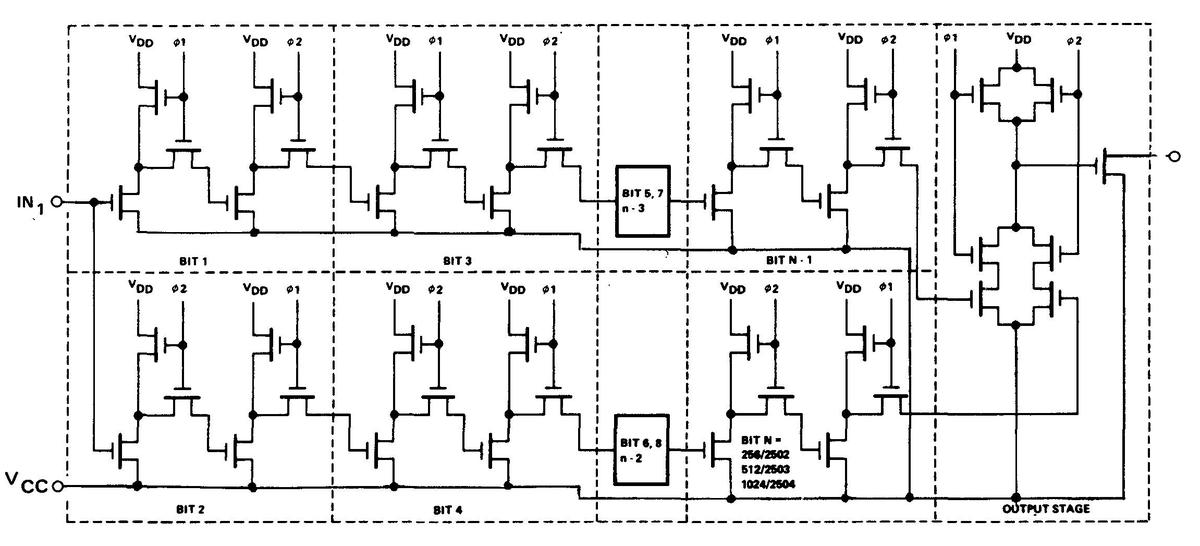
  6. The schematic of the chip is shown below. Notice the upper and lower shift registers, which run on opposite clock phases. Apart from the 6-transistor shift-register stages, the only circuitry is the output stage that merges the two results and drives the output pin.

    Schematic of the chip. Click for a larger image. From the 1972 databook.

    Schematic of the chip. Click for a larger image. From the 1972 databook.


  7. Another major improvement in integrated circuits was the introduction of CMOS, which used NMOS and PMOS transistors together, with much lower power consumption. By the 1980s, processors such as the Intel 80386 (1985) and Motorola 68030 (1987) used CMOS. CMOS is still used in modern integrated circuits. 

  8. In the mid-1970s, ion implantation technology allowed the creation of depletion-mode transistors. These transistors could be used as pull-up elements, called depletion loads. Since depletion-load transistors could operate faster and with less current, they rapidly became a standard part of MOS integrated circuits, until replaced by CMOS in the 1980s. The Zilog Z80 and Intel 2102 SRAM were two early chips that used depletion loads. 

  9. You might think that the inverter circuit will result in a short circuit between Vdd and Vcc when both the input and the clock are high. However, the pull-up transistor is designed to produce a weak current, so the other transistor can still pull the output low. This current results in relatively high power consumption for PMOS or NMOS circuitry, a problem that is fixed by CMOS. 

  10. The 256×4 2502B chip required a 16-pin package, rather than the 8-pin package of other chips, due to the additional input and output pins.