Intel introduced the 8086 microprocessor in 1978, and its influence still remains through the popular x86 architecture. The 8086 was a fairly complex microprocessor for its time, implementing instructions in microcode with pipelining to improve performance. This blog post explains the microcode operations for a particular instruction, "ADD immediate". As the 8086 documentation will tell you, this instruction takes four clock cycles to execute. But looking internally shows seven clock cycles of activity. How does the 8086 fit seven cycles of computation into four cycles? As I will show, the trick is pipelining.
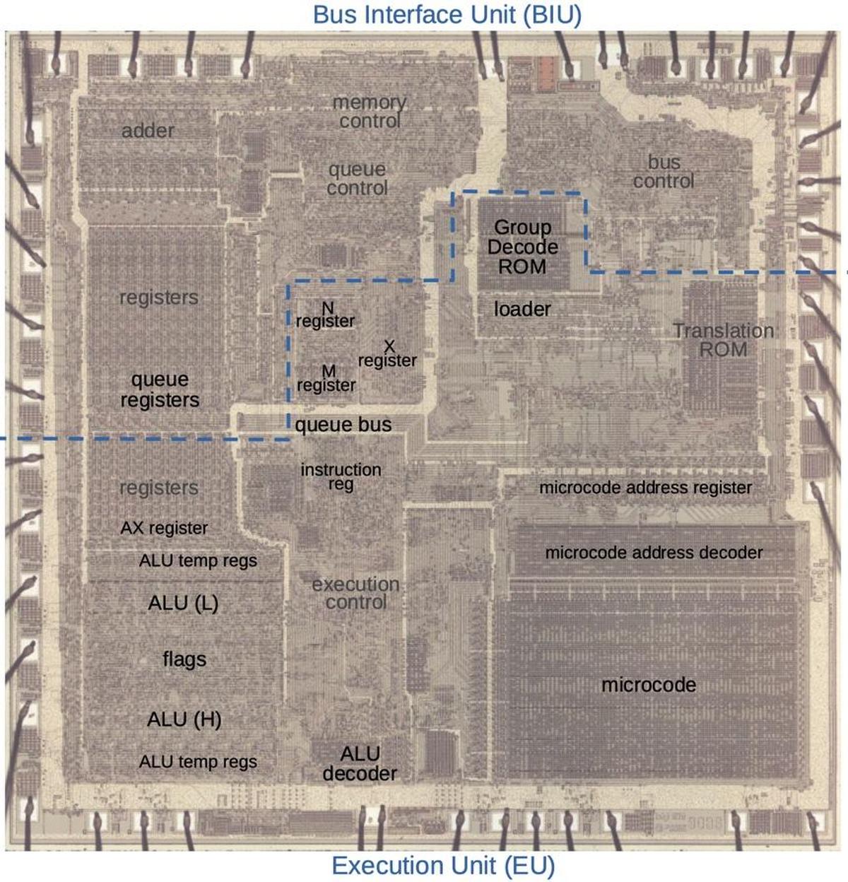
The die photo below shows the 8086 microprocessor under a microscope. The metal layer on top of the chip is visible, with the silicon and polysilicon mostly hidden underneath. Around the edges of the die, bond wires connect pads to the chip's 40 external pins. Architecturally, the chip is partitioned into a Bus Interface Unit (BIU) at the top and an Execution Unit (EU) below, which will be important in the discussion. The Bus Interface Unit handles memory accesses (including instruction prefetching), while the Execution Unit executes instructions. The functional blocks labeled in black are the ones that are part of the discussion below. In particular, the registers and ALU (Arithmetic/Logic Unit) are at the left and the large microcode ROM is in the lower-right.
Microcode for "ADD"
Most people think of machine instructions as the basic steps that a computer performs. However, many processors (including the 8086) have another layer of software underneath: microcode. The motivation is that instructions usually require multiple steps inside the processor. One of the hardest parts of computer design is creating the control logic that directs the processor for each step of an instruction. The straightforward approach is to build a circuit from flip-flops and gates that moves through the various steps and generates the control signals. However, this circuitry is complicated, error-prone, and hard to design.
The alternative is microcode: instead of building the control circuitry from complex logic gates, the control logic is largely replaced with code. To execute a machine instruction, the computer internally executes several simpler micro-instructions, specified by the microcode. In other words, microcode forms another layer between the machine instructions and the hardware. The main advantage of microcode is that it turns the processor's control logic into a programming task instead of a difficult logic design task.
The 8086 uses a hybrid approach: although the 8086 uses microcode, much of the instruction functionality is implemented with gate logic. This approach removed duplication from the microcode and kept the microcode small enough for 1978 technology. In a sense the microcode is parameterized. For instance, the microcode can specify a generic ALU operation, and the gate logic determines from the instruction which ALU operation to perform. Likewise, the microcode can specify a generic register and the gate logic determines which register to use. The simplest instructions (such as prefixes or condition-code operations) don't use microcode at all. Although this made the 8086's gate logic more complicated, the tradeoff was worthwhile.
The 8086's microcode was disassembled by Andrew Jenner (link) from my die photos, so we can see exactly what micro-instructions the 8086 is running for each machine instruction. In this post, I will focus on the ADD instruction, since it is fairly straightforward. In particular, the "ADD AX, immediate" instruction contains a 16-bit value that is added to the value in the 16-bit AX register. This instruction consists of three bytes: the opcode 05, followed by the two-byte immediate value. (An "immediate" value is included in the instruction, rather than coming from a register or memory location.)
This ADD instruction is implemented in the 8086's microcode as four micro-instructions, shown below. Each micro-instruction specifies a move operation across the internal ALU bus. It also specifies an action. In brief, the first two instructions get the immediate argument from the prefetch queue. The third instruction gets the argument from the AX register and starts the ALU (Arithmetic/Logic Unit) operation. The final instruction stores the result into the AX register and updates the condition flags.
µ-address    move        action
   018    Q → tmpBL     L8    2
   019    Q → tmpBH
   01a    M → tmpA      XI    tmpA, NXT
   01b    Σ → M         RNI   FLAGS
In detail, the first instruction moves a byte from the prefetch queue (Q) to one of the ALU's temporary registers, specifically the low byte of the tmpB register.
(The ALU has three temporary registers to hold arguments: tmpA, tmpB, and tmpC.
These temporary registers are invisible to the programmer and are unrelated to the AX, BX, CX registers.)
Likewise, the second instruction fetches the high byte of the immediate value from the queue and stores it in the high byte of the ALU's tmpB register.
The action in the first micro-instruction, L8, will branch to step 2 (01a) if the instruction specifies an 8-bit operation, skipping the load of the high byte.
Thus, the same microcode supports the 8-bit and 16-bit ADD instructions.1
The third micro-instruction is more complicated. The move section moves the AX register's contents (indicated by M) to the accumulator's tmpA register, getting both arguments ready for
the operation. XI tmpA starts an ALU operation, in this case adding tmpA to tmpB.2
Finally, NXT indicates that this is the next-to-last micro-instruction, as will be discussed below.
The last micro-instruction stores the ALU's result (Σ) into the AX register.
The end of the microcode for this machine instruction is indicated by RNI (Run Next Instruction). Finally, FLAGS causes the 8086's condition flags register to be updated,
indicating if the result is zero, negative, and so forth.
You may have noticed that the microcode doesn't explicitly specify the ADD operation or the AX register, using XI and M instead.
This illustrates the "parameterized" microcode mentioned earlier.
The microcode specifies a generic ALU operation with XI,3 and the hardware fills in the particular ALU operation from bits 5-3 of the machine instruction.
Thus, the microcode above can be used for addition, subtraction, exclusive-or, comparisons, and four other arithmetic/logic operations.
The other parameterized aspect is the generic M register specification.
The 8086's instruction set has a flexible way of specifying registers for the source and destination of an operation:
registers are often specified by a "Mod R/M" byte, but can also be specified by bits in the first opcode.
Moreover, many instructions have a bit to switch the source and destination, and another bit to specify an 8-bit or 16-bit register.
The microcode can ignore all this; a micro-instruction uses M and N for the source and destination registers, and the hardware handles the details.4
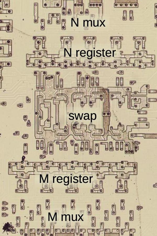
The M and N values are implemented by 5-bit registers that are invisible to the programmer and specify the "real" register to use. The diagram below shows how they appear on the die.
Pipelining
The 8086 documentation says this ADD instruction takes four clock cycles, and as we have seen, it is implemented with four micro-instructions. One micro-instruction is executed per clock cycle, so the timing seems straightforward. The problem, however, is that a micro-instruction can't be completed in one clock cycle. It takes a clock cycle to read a micro-instruction from the microcode ROM. Sending signals across an internal bus typically takes a clock cycle and other actions take more time. So a typical micro-instruction ends up taking 2½ clock cycles from start to end. One solution would be to slow down the clock, so the micro-instruction can complete in one cycle, but that would drastically reduce performance. A better solution is pipelining the execution so a micro-instruction can complete every cycle.5
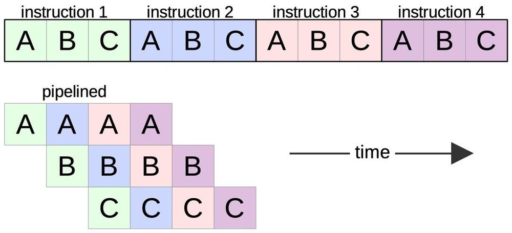
The idea of pipelining is to break instruction processing into "stages", so different stages can work on different instructions at the same time. It's sort of like an assembly line, where a particular car might take an hour to manufacture, but a new car comes off the assembly line every minute. The diagram below shows a simple example. Suppose executing an instruction requires three steps: A, B, and C. Executing four instructions, as shown at the top would take 12 steps in total.
However, suppose the steps can execute independently, so step B for one instruction can execute at the same time as step A for another instruction. Now, as soon as instruction 1 finishes step A and moves on to step B, instruction 2 can start step A. Next, instruction 3 starts step A as instructions 2 and 1 move to steps B and C respectively. The first instruction still takes 3 time units to complete, but after that, an instruction completes every time unit, providing a theoretical 3× speedup.6 In a bit, I will show how the 8086 uses the idea of pipelining.
The prefetch queue
The 8086 uses instruction prefetching to improve performance. Prefetching is not the focus of this article, but a brief explanation is necessary. (I wrote about the prefetch circuitry in detail earlier.) Memory accesses on the 8086 are relatively slow (at least four clock cycles), so we don't want to wait every time the processor needs a new instruction. The idea behind prefetching is that the processor fetches future instructions from memory while the CPU is busy with the current instruction. When the CPU is ready to execute the next instruction, hopefully the instruction is already in the prefetch queue and the CPU doesn't need to wait for memory. The 8086 appears to be the first microprocessor to implement prefetching.
In more detail, the 8086 fetches instructions into its prefetch queue asynchronously from instruction execution: The "Bus Interface Unit" performs prefetches, while the "Execution Unit" executes instructions. Prefetched instructions are stored in the 6-byte prefetch queue. The Q bus (short for "Queue bus") provides bytes, one at a time, from the prefetch queue to the Execution Unit.7 If the prefetch queue doesn't have a byte available when the Execution Unit needs one, the Execution Unit waits until the prefetch circuitry can complete a memory access.
The loader
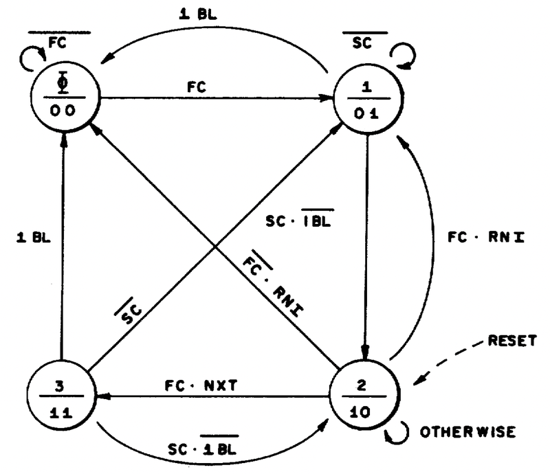
To decode and execute an instruction, the Execution Unit must get instruction bytes from the prefetch queue, but this is not entirely straightforward. The main problem is that the prefetch queue can be empty, blocking execution. Second, instruction decoding is relatively slow, so for maximum performance, the decoder needs a new byte before the current instruction is finished. A circuit called the "loader" solves these problems by using a small state machine (below) to efficiently fetch bytes from the queue at the right time.
The loader generates two timing signals that synchronize instruction decoding and microcode execution with the prefetch queue. The FC (First Clock) indicates that the first instruction byte is available, while the SC (Second Clock) indicates the second instruction byte. Note that the First Clock and Second Clock are not necessarily consecutive clock cycles because the first byte could be the last one in the queue, delaying the Second Clock.
At the end of a microcode sequence, the Run Next Instruction (RNI) micro-operation causes the loader to fetch the next machine instruction.
However, microcode execution would be blocked for a cycle due to the delay of fetching and decoding the next instruction.
In many cases, this can be avoided: if the microcode knows that it is one micro-instruction away from finishing,
it issues a Next-to-last (NXT) micro-operation so the loader can start loading the next instruction before the previous instruction finishes.
As will be shown in the next section,
this usually allows micro-instructions to run without interruption.
Instruction execution
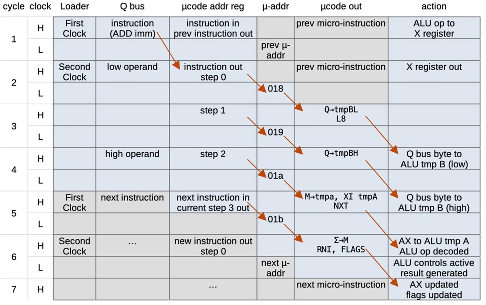
Putting this all together, we can see how the ADD instruction is executed, cycle by cycle. Each clock cycle starts with the clock high (H) and ends with the clock low (L).8 The sequence starts with the prefetch queue supplying the ADD instruction across the Q bus in cycle 1. The loader indicates that this is First Clock and the instruction is loaded into the microcode address register. It takes a clock cycle for the address to exit the address register (as indicated by an arrow) along with the microcode counter value indicating step 0. To remember the ALU operation, bits 5-3 of the instruction are saved in the internal X register (unrelated to the AX register).
In cycle 2, the prefetch queue has supplied the second byte of the instruction so the loader indicates Second Clock. In the second half of cycle 2, the microcode address decoder has converted the instruction-based address to the micro-address 018 and supplies it to the microcode ROM.
In cycle 3, the microcode ROM outputs the micro-instruction at micro-address 018: Q→tmpBL, which will move a byte from the prefetch queue bus (Q bus) to the low byte of the ALU temporary B register, as described earlier.
It takes a full clock cycle for this action to take place, as the byte traverses buses to reach the register.
This micro-instruction also generates the L8 micro-op, which will branch if an 8-bit operation is taking place.
As this is a 16-bit operation, no branch takes place.9
Meanwhile, the microcode address register moves to step 1, causing the decoder to produce the micro-address 019.
In cycle 4,
the prefetch queue provides a new byte, the high byte of the immediate value.
The microcode ROM outputs the micro-instruction at micro-address 019: Q→tmpBH, which will move this byte from the prefetch queue bus to the high byte of the ALU temporary B register.
As before, it takes a full cycle for this move to complete.
Meanwhile, the microcode address register moves to step 2, causing the decoder to produce the micro-address 01a.
In cycle 5,
the microcode ROM outputs the micro-instruction at micro-address 01a: M→tmpA,XI tmpA,NXT.
Since the M (source) register specifies AX, the contents of the AX register will be moved into the ALU tmpA register, but this will take a cycle to complete.
The XI tmpA part starts decoding the ALU operation saved in the X register, in this case ADD.
Finally, NXT indicates that the next micro-instruction is the last one in this instruction.
In combination with the next instruction on the Q bus, this causes the loader to issue First Clock. This starts execution of the next machine instruction, even though the current instruction is still executing.
In cycle 6,
the microcode ROM outputs the micro-instruction at micro-address 01b: Σ→M,RNI.
This will store the ALU output into the register indicated by M (i.e. AX), but not yet.
In the first half of cycle 6, the ALU decoder determines the ALU control signals that will cause an ADD to take place.
In the second half of cycle 6, the ALU receives these control signals and computes the sum.
The RNI (Run Next Instruction) and the second instruction byte from the prefetch queue cause the loader to issue Second Clock, and the micro-address for
the next machine instruction is sent to the microcode ROM.
Finally, in cycle 7, the sum is written to the AX register and the flags are updated, completing the ADD instruction. Meanwhile, the next instruction is well underway with its first micro-instruction being executed.
As you can see, execution of a micro-instruction is pipelined, with three full clock cycles from the arrival of an instruction until the first
micro-instruction completes in cycle 4.
Although this system is complex, in the best case it achieves the goal of running a micro-instruction each cycle, without gaps.
(There are gaps in some cases, most commonly when the prefetch queue is empty.
A gap will also occur if the microcode control flow doesn't allow a NXT micro-instruction to be issued.
In that case, the loader can't issue First Clock until the RNI micro-instruction is issued, resulting in a delay.)
Conclusions
The 8086 uses multiple types of pipelining to increase performance. I've focused on the pipelining at the microcode level, but the 8086 uses at least four interlocking types of pipelining. First, microcode pipelining allows micro-instructions to complete at the rate of one per clock cycle, even though it takes multiple cycles for a micro-instruction to complete. Admittedly, this pipeline is not very deep compared to the pipelines in RISC processors; the 8086 designers called the overlap in the microcode ROM a "sort of mini-pipeline."10
The second type of pipelining overlaps instruction decoding and execution. Instruction decoding is fairly complicated on the 8086 since there are many different formats of instructions, usually depending on the second byte (Mod R/M). The loader coordinates this pipelining, issuing the First Clock and Second Clock signals so decoding on the next instruction can start before the previous instruction has completed. Third is the prefetch queue, which overlaps fetching instructions from memory with execution. This is accomplished by partitioning the processor into the Bus Interface Unit and the Execution Unit, with the prefetch queue in between. (I recently wrote about instruction prefetching in detail.)
There's a final type of pipelining that I haven't discussed. Inside the memory access sequence, computing the memory address from a segment register and offset is overlapped with the previous memory access. The result is that memory accesses appear to take four cycles, even though they really take six cycles. I plan to write more about memory access in a later post.
The 8086 was a large advance in size, performance, and architecture compared to earlier microprocessors such as the Z80 (1976), 8085 (1977), and 6809 (1978). As well as moving to 16 bits, the 8086 had a considerably more complex architecture with instruction prefetching and microcode, among other features. At the same time, the 8086 avoided the architectural overreach of Intel's ill-fated iAPX 432, a complex processor that supported garbage collection and objects in hardware. Although the 8086's architecture had flaws, it was a success and led to the x86 architecture, still dominant today.
I plan to continue reverse-engineering the 8086 die so follow me on Twitter @kenshirriff or RSS for updates. I've also started experimenting with Mastodon recently as @oldbytes.space@kenshirriff. If you're interested in the 8086, I wrote about the 8086 die, its die shrink process and the 8086 registers earlier.
Notes and references
-
The lowest bit of many 8086 instructions selects if the instruction operates on a byte or a word. Thus, many instructions in the instruction set appear in pairs. The support for byte operations gave the 16-bit 8086 processor compatibility with the older 8-bit 8080, if assembly code was suitably translated. ↩
-
The microcode for an ALU operation can select the first operand from tmpA, tmpB, or tmpC. The second operand is always tmpB. ↩
-
I don't know why Intel used XI to indicate the ALU opcode. I don't think it's the Greek letter Ξ, although they did use Σ (sigma) for the ALU output. The opcode is stored in the X register, so maybe XI is X Instruction? (It's also unclear why the register is called X.) ↩
-
Normally, the internal M register specifies the source register and the N register specifies the destination register, and these two registers are loaded from the instruction. However, some instructions only use the A or AX register, depending on whether the instruction acts on bytes or words. These instructions are the ALU immediate instructions, accumulator move instructions, string instructions, and the TEST, IN, and OUT instructions. For these instructions, the Group Decode ROM activates a signal that forces the M register to specify the AX register for a 16-bit operation, or the A register for an 8-bit operation. Thus, by specifying the M register in the microcode above, the same microcode is used for instructions with an 8-bit immediate argument or a 16-bit immediate argument. This also illustrates how the designers of the 8086 kept the microcode small by moving a lot of logic into hardware. ↩
-
I should mention that the pipelining in the 8086 is completely different from the parallelism in modern superscalar CPUs. The 8086 is executing instructions linearly, step-by-step, even though instructions overlap. There is only one execution path and no speculative execution, for instance. ↩
-
I showed a theoretical speedup from pipelining. Several issues make the real speedup smaller. First, the steps of an instruction typically don't take the same amount of time, so you're limited by the slowest step. Second, the overhead to handle the steps adds some delay. Finally, conflicts between instructions and other "hazards" may prevent overlap in various cases. ↩
-
The interaction between the prefetch queue and the Execution Unit is a "push" model rather than a "pull" model. If the prefetch queue contains a byte, the prefetch circuitry puts the byte on the Q bus and lets the Execution Unit know that a byte is available. The Execution Unit signals the prefetch circuitry when it uses a byte, and the prefetch queue moves to the next byte in the queue. If the Execution Unit needs a byte and it isn't ready, it blocks until a byte is available. The prefetch queue loads new words as it empties, when the memory bus isn't in use for other purposes. ↩
-
The 8086 is active during both phases (low and high) of the clock, with things happening both while the clock is high and while it is low. One unusual feature of the 8086 is that the clock signal is asymmetrical with a 33% duty cycle, so the clock is low for twice as long as the clock is high. In other words, the 8086 does twice as much (by time) during the low part of the clock cycle as during the high part of the clock cycle. There are multiple reasons why actions take a full clock cycle to complete. Much of the circuitry uses edge-triggered flip-flops to hold state. These latch data on one clock edge and move data internally during the other part of the clock. (The 8086 uses both positive-edge and negative-edge triggered flip flops; some latch when the clock goes high and others latch when the clock goes low.) Many control signals have their voltage level boosted by a bootstrap driver circuit, driven by the clock.
Many buses are precharged during one clock phase and then transmit a signal during the other phase. The motivation behind precharging the bus is that NMOS transistors are much better at pulling a line low than pulling it high (i.e. they can provide more current). This especially affects buses because they have relatively high capacitance due to their length, so pulling the bus high is slow. Thus, the bus is "leisurely" precharged to a high state during one clock phase, and then it can be rapidly pulled low (if the bit is a 0) and transmit the data during the other clock phase. ↩
-
You might expect that the 8-bit ADD would be faster than the 16-bit ADD since it is a 2-byte instruction instead of a 3-byte instruction and one micro-instruction is skipped. However, both the 8-bit and the 16-bit ADD instructions take 4 cycles. The reason is that branching to a new micro-instruction requires updating the microcode address register, which takes a clock cycle, resulting in a wasted clock cycle where no micro-instruction is executed. (Specifically, the next micro-instruction is on the way, so it is blocked by the ROM Enable (ROME) signal going low.) The result of this is that the branch for an 8-bit ADD costs an extra cycle, which cancels out the saved cycle. (In practice, the 16-bit instruction might be slower because it needs one more byte from the prefetch queue, which could cause a delay.) Just as a branch in the machine instructions can cause a delay (a "bubble") in the instruction pipeline, a branch in the microcode causes a delay in the micro-instruction pipeline. ↩
-
The design decisions for the 8086 are described in: J. McKevitt and J. Bayliss, "New options from big chips," in IEEE Spectrum, vol. 16, no. 3, pp. 28-34, March 1979, doi: 10.1109/MSPEC.1979.6367944. ↩
11 comments:
This fantastic low-level dissection of the instruction dispatch machinery reminded me of when my colleagues and I implemented a fast(er) byte code interpreter for UCSD p-system by adding the bytecode to a base in AX, then something like MOV CS, AX; JMP 0; NOP(s). Execution would transfer to some number of bytes into a 16-byte segment for each possible bytecode... many simple opcodes and jump right back to fetch the next bytecode. I don't remember the exact latencies but it was noticeably better than a computed indirect jump. Because the prefetches and pipelines varied between models, we had to profile the CPU before selecting an implementation. This didn't work at all anymore on some clones and in protected mode, so we eventually removed this hack altogether.
Oops. "many simple opcodes and jump right back to fetch the next bytecode"
-> Many simple bytecodes would fit in the remaining bytes and jump right back to fetch the next bytecode.
I would have guessed "execute integer op" for XI.
Nice analysis, my elec eng degree in the very early 90s was all about making cpus silicon to microcode either cisc 8086 or motorola or non microcode risc mips and uk special transputers at the time, as your dissecting x86, their was a rumour that intel had made a 486 run async no gate clock require it had double the number of gates ran alot faster, this was in silicon glen Scotland uk, you probably find out if true?
MOV CS only works on an Intel 8088/8086. It doesn't work on e.g. a NEC V20/30, and on an 186 and later causes an exception. Also, it empties the prefetch queue, so any JMP 0 isn't executed - the CPU jumps to exactly the next IP but in a different segment. So the hack is possible, but only on a very limited set of CPUs, and it needs very specific code set-up.
>but only on a very limited set of CPUs
Absolutely, but the IBM PC and its clones with 8088's were completely dominant for years and slow as molasses.
Pipelining was a fairly common technique for microcoded CPUs. The Xerox Alto's (32-bit wide) microcode engine certainly had some pipelining, including delayed branches.
In the series of articles so far (will there be a book?), you've detailed how the prefetch unit can supply instructions to the execution unit without the queue needing to be full; and how performance is impressively optimised by microcode pipelining.
Ironically, this makes me more confused as to why 8086 jump instructions are so slow, at 14 cycles per jump (slower on an 8088). Jumps will occur about 25% of the time on an 8086, so as I understand it (based on my worn copy of "Computer Architecture, A Quantitive Approach, Second Edition"); this represents quite a performance hit given that even 8-bit CPUs like the Z80 and the 6502 can perform them much quicker (12, 3 cycles respectively) without the same degree of pipelining or prefetching.
I had always imagined it was due to the prefetch queue getting flushed and having to wait to be filled, but really it only need the first entry, which can be as little as 4 clock cycles away.
@Snial:
Reason is prefetch handling instructions.
Two loads, then suspension of prefetch, correction to PC, add offset and then flush queue. All jumps have similar execution flow (sometimes only prefetch instructions, sometimes multiple loads).
You can see it in Reengine's transcription.
"One unusual feature of the 8086 is that the clock signal is asymmetrical with a 33% duty cycle" --- this isn't *quite* correct. Check the timings specified in the datasheet - running at max clock rate with 33% duty cycle actually ends up being *slightly* out of spec: 33% of an 8MHz cycle is 42ns, while the data sheet says minimum high time is 44ns. I believe the 33% figure comes about because this is what the 8284 implements so is what most systems actually use, and it's not likely that being 2ns out of spec would be a problem, but if you want to be pedantically correct and run at maximum speed, you need at least a 35.2% duty cycle and at most a 45.6% duty cycle (assuming zero time for the signal to rise and fall, so realistically as close to 40% as you can manage). Alternatively, you can slow the clock rate to 7.5Mhz and use 33%.
@Anonymous: "rumour that intel had made a 486 run async no gate clock require it had double the number of gates ran alot faster"
Note that 486s are notoriously easy to overclock, and were the first chip where Intel supported running the core clock at a different speed to the bus clock, so it's entirely plausible that Intel had prototype chips with (e.g.) programmable clock multipliers and no other change to the core implementation that ran at substantially higher rates than officially supported. This is a chip that with only two process shrinks went from 20MHz all the way up to 100MHz. I doubt Intel ever produce an async version of the 486 -- it would be difficult to guarantee reliability, so it would never have been destined for a commercial product, and for an internal research project you'd probably pick a simpler target.
My guess for the meaning of 'XI' is that the 'X' is used as a wildcard for the ALU operation ('ADD', 'SUB', 'CMP', etc.) and 'I' for immediate. In other words, XI means do whichever ALU operation with immediate mode addressing.
Post a Comment