The 8086 microprocessor is one of the most important chips ever created; it started the x86 architecture that still dominates desktop and server computing today. I've been reverse-engineering its circuitry by studying its silicon die. One of the most unusual circuits I found is a "bootstrap driver", a way to boost internal signals to improve performance.1
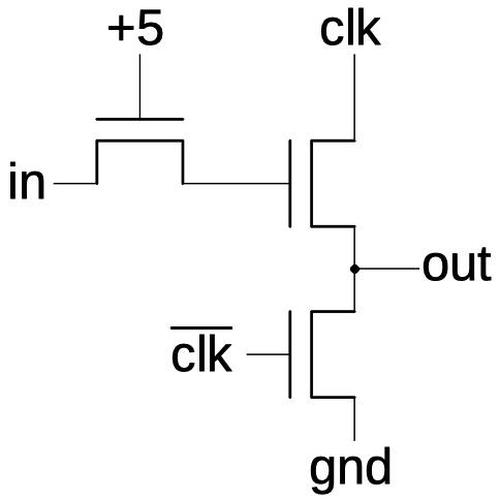
This circuit consists of just three NMOS transistors, amplifying an input signal to produce an output signal, but it doesn't resemble typical NMOS logic circuits and puzzled me for a long time. Eventually, I stumbled across an explanation:2 the "bootstrap driver" uses the transistor's capacitance to boost its voltage. It produces control pulses with higher current and higher voltage than otherwise possible, increasing performance. In this blog post, I'll attempt to explain how the tricky bootstrap driver circuit works.
NMOS transistors
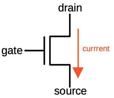
The 8086 is built from MOS transistors (MOSFETs), specifically NMOS transistors. Understanding the bootstrap driver requires some understanding of these transistors. If you're familiar with MOSFETs as components, they have source and drain pins and current flows from the drain to the source, controlled by the gate pin. Most of the time I treat an NMOS transistor as a digital switch between the drain and the source: a 1 input turns the transistor on, closing the switch, while a 0 turns the transistor off. However, for the bootstrap driver, we must consider the MOSFET in a bit more detail.
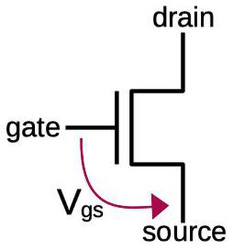
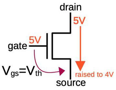
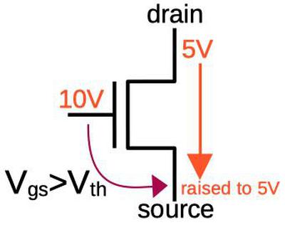
The important aspect of the gate is the difference between the gate voltage and the (typically lower) source voltage; this is denoted as Vgs. Without going into semiconductor physics, a slightly more accurate model is that the transistor turns on when the voltage between the gate and the source exceeds the fixed threshold voltage, Vth. This creates a conducting channel between the transistor's source and drain. Thus, if Vgs > Vth, the transistor turns on and current flows. Otherwise, the transistor turns off and no current flows.
The threshold voltage has an important consequence for a chip such as the 8086. The 8086, like most chips of that era, used a 5-volt power supply. The threshold voltage depends on manufacturing characteristics, but I'll use 1 volt as a typical value.3 The result is that if you put 5 volts on the drain and on the gate, the transistor can pull the source up to about 4 volts, but then Vgs falls to the threshold voltage and the transistor stops conducting. Thus, the transistor can't pull the source all the way up to the 5-volt supply, but falls short by a volt on the output. In some circumstances this is a problem, and this is the problem that the bootstrap driver fixes.
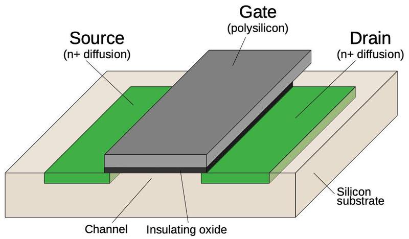
If you get a transistor as a physical component, the source and drain are not interchangeable. However, in an integrated circuit, there is no difference between the source and the drain, and this will be important.4 The diagram below shows how a MOSFET is constructed on the silicon die. The source and drain consist of regions of silicon doped with impurities to change their property. Between them is a channel of undoped silicon, which normally does not conduct. Above the channel is the gate, made of a special type of silicon called polysilicon. The voltage on the gate controls the conductivity of the channel. A very thin insulating layer separates the gate from the channel. As a side effect, the insulating layer creates some capacitance between the gate and the underlying silicon.
Basic NMOS circuits
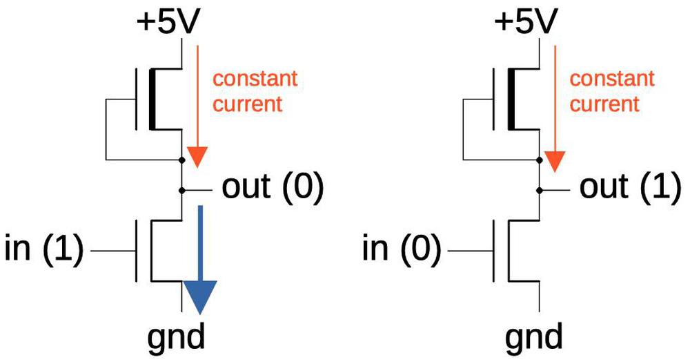
Before getting to the bootstrap driver, I'll explain how a basic inverter is implemented in an NMOS chip like the 8086. The inverter is built from two transistors: a normal transistor on the bottom, and a special load transistor on top that acts like a pull-up resistor, providing a small constant current.5 With a 1 input, the lower transistor turns on, pulling the output to ground to produce a 0 output. With a 0 input, the lower transistor turns off and the current from the upper transistor drives the output high to produce a 1 output. Thus, the circuit implements an inverter: producing a 1 when the input is 0 and vice versa.
The disadvantage of this inverter circuit is that when it produces a 0 output, current continuously flows through the load transistor and the lower transistor to ground. This wastes power, leading to high power consumption for NMOS circuitry. (To solve this, CMOS circuitry took over in the 1980s and is used in modern microprocessors.) This also limits the current that the inverter can provide.
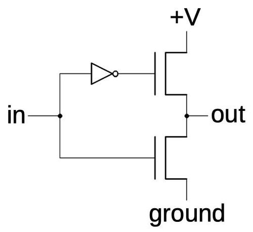
If a gate needs to provide a relatively large current, for instance to drive a long bus inside the chip, a more complex circuit is used, the "superbuffer". The superbuffer uses one transistor to pull the output high and a second transistor to pull the output low.6 Because only one transistor is on at a time, a high-current output can be produced without wasting power. There are two disadvantages of the superbuffer, though. First, the superbuffer requires an inverter to control the high-side transistor, so it uses considerably more space on the die. Second, the superbuffer can't pull the high output all the way up; it loses a volt due to the threshold voltage as described earlier.
The bootstrap driver
In some circumstances, you want both a high-current output, and the full output voltage. One example is connecting a register to an internal bus. Since the 8086 is a 16-bit chip, it uses 16 transistors for the bus connection. Driving 16 transistors in parallel requires a fairly high current. But the bus transistors are "pass" transistors, which lose a volt due to the threshold voltage, so you want to start with the full voltage, not already down one volt. To provide both high current and the full voltage, bootstrap drivers are used to control the buses, as well as similar tasks such as ALU control.
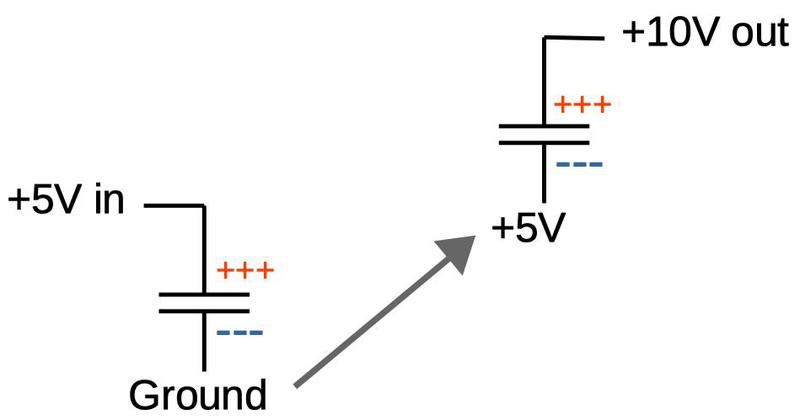
The concept behind the bootstrap driver is to drive the gate voltage significantly higher than 5 volts, so even after losing the threshold voltage, the transistor can produce the full 5-volt output.7 The higher voltage is generated by a charge pump, as illustrated below. Suppose you charge a capacitor with 5 volts. Now, disconnect the bottom of the capacitor from ground, and connect it to +5 volts. The capacitor is still charged with 5 volts, so now the high side is at +10 volts with respect to ground. Thus, a capacitor can be used to create a higher voltage by "pumping" the charge to a higher level.
The idea of the bootstrap driver is to attach a capacitor to the gate and charge it to 5 volts. Then, the low side of the capacitor is raised to 5 volts, boosting the gate side of the capacitor to 10 volts. With this high voltage on the gate, the threshold voltage is easily exceeded and the transistor can pass the full 5 volts from the drain to the source, producing a 5-volt output.
In the 8086 bootstrap driver,8 an explicit capacitor is not used.9 Instead, the transistor's inherent capacitance is sufficient. Due to the thin insulating oxide layer between the gate and the underlying silicon, the gate acts as the plate of a capacitor relative to the source and drain. This "parasitic" capacitance is usually a bad thing, but the bootstrap driver takes advantage of it.
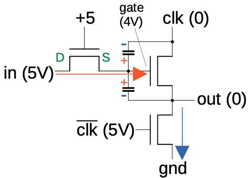
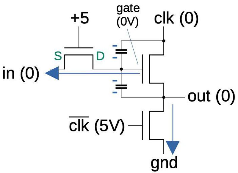
The diagrams below show how the bootstrap driver works. Unlike an inverter, the bootstrap driver is controlled by the chip's clock, generating an output only when the clock is high. In the first diagram, we assume that the input is a 1 and the clock is low (0). Two things happen. First, the inverted clock turns on the bottom transistor, pulling the output to ground. Second, the 5V input passes through the first transistor; the left side of the transistor acts as the drain and the right side as the source. Due to the threshold voltage, a volt is "lost" so about 4 volts reaches the gate of the second transistor. Since the source and drain of the second transistor are at 0 volts, the gate capacitors are charged with 4 volts. (Recall that these are not explicit capacitors, but are parasitic capacitors.)
In the next step, the clock switches state and things become more interesting. The second transistor is on due to the voltage on the gate, so current flows from the clock to the output. In a "normal" circuit, the output would rise to 4 volts, losing a volt due to the threshold voltage of the second transistor. However, as the output voltage rises, it boosts the voltage on the gate capacitors and thus raises the gate voltage. The increased gate voltage allows the output voltage to rise above 4 volts, pushing the gate voltage even higher, until the output reaches 5 volts.10 Thus, the bootstrap driver produces a high-current output with the full 5 volts.
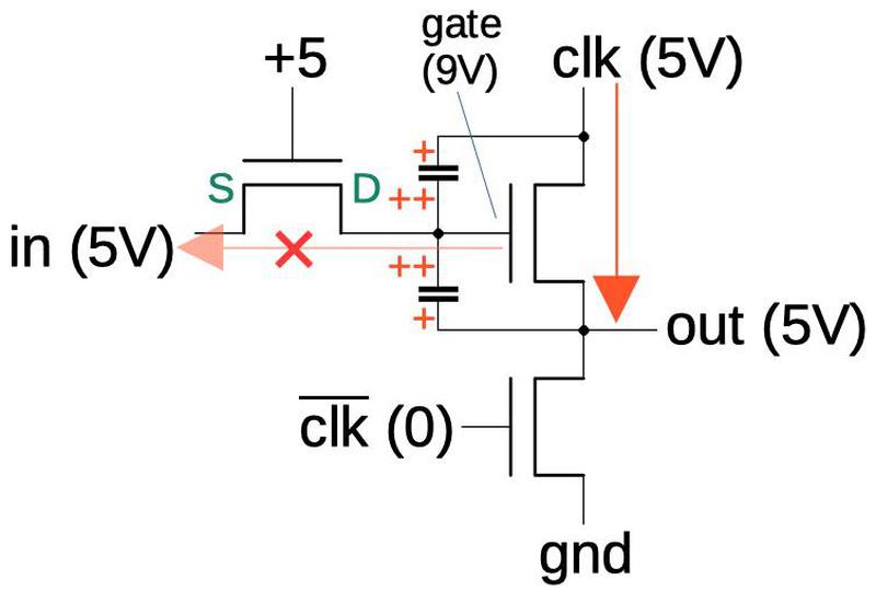
An important factor is that the first transistor now has a higher voltage on the right than on the left, so the source and drain switch roles. Since the transistor has 5 volts on the gate and on the (now) source, Vgs is 0 and current can't flow. Thus the first transistor blocks current flow from the gate, keeping the gate at its higher voltage. This is the critical role of the first transistor in the bootstrap driver, acting as a diode to block current flow out of the gate.
The diagram below shows what happens when the clock switches state again, assuming a low input. Now the first transistor's source voltage drops, making Vgs large and turning the transistor on. This allows the second transistor's gate voltage to flow out. Note that the first transistor is no longer acting as a diode, since current can flow in the "reverse" direction. The other important action in this clock phase is that the bottom transistor turns on, pulling the output low. These actions discharge the gate capacitance, preparing it for the next bootstrap cycle.
The 8086 die
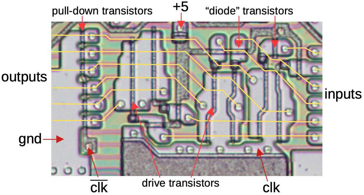
Now that I've explained the theory, how do bootstrap drivers appear on the silicon die of the 8086? The diagram below shows six drivers that control the ALU operation.11 There's a lot happening in this diagram, but I'll try to explain what's going on. For this photo, I removed the metal layer with acid to reveal the silicon underneath; the yellow lines show where the metal wiring was. The large pinkish regions are doped silicon, while the gray speckled lines are polysilicon on top. The greenish and reddish regions are undoped silicon, which doesn't conduct and can be ignored. A transistor is formed where a polysilicon line crosses silicon, with the source and drain on opposite sides. Note that some transistors share the source or drain region with a neighboring transistor, saving space. The circles are vias, connections between the metal and a lower layer.
The drivers start with six inputs at the right. Each input goes through a "diode" transistor with the gate tied to +5V. I've labeled two of these transistors and the other four are scattered around the image. Next, each signal goes to the gate of one of the drive transistors. These six large transistors pass the clock to the output when turned on. Note that the clock signal flows through large silicon regions, rather than "wires". Finally, each output has a pull-down transistor on the left, connecting it to ground (another large silicon region) under control of the inverted clock. The drive transistors are much larger than the other transistors, so they can provide much more current. Their size also provides the gate capacitance necessary for the operation of the bootstrap driver.
Although the six drivers in this diagram are electrically identical, each one has a different layout instead of repeating the same layout six times. This demonstrates how the layout has been optimized, moving transistors around to use space most efficiently.
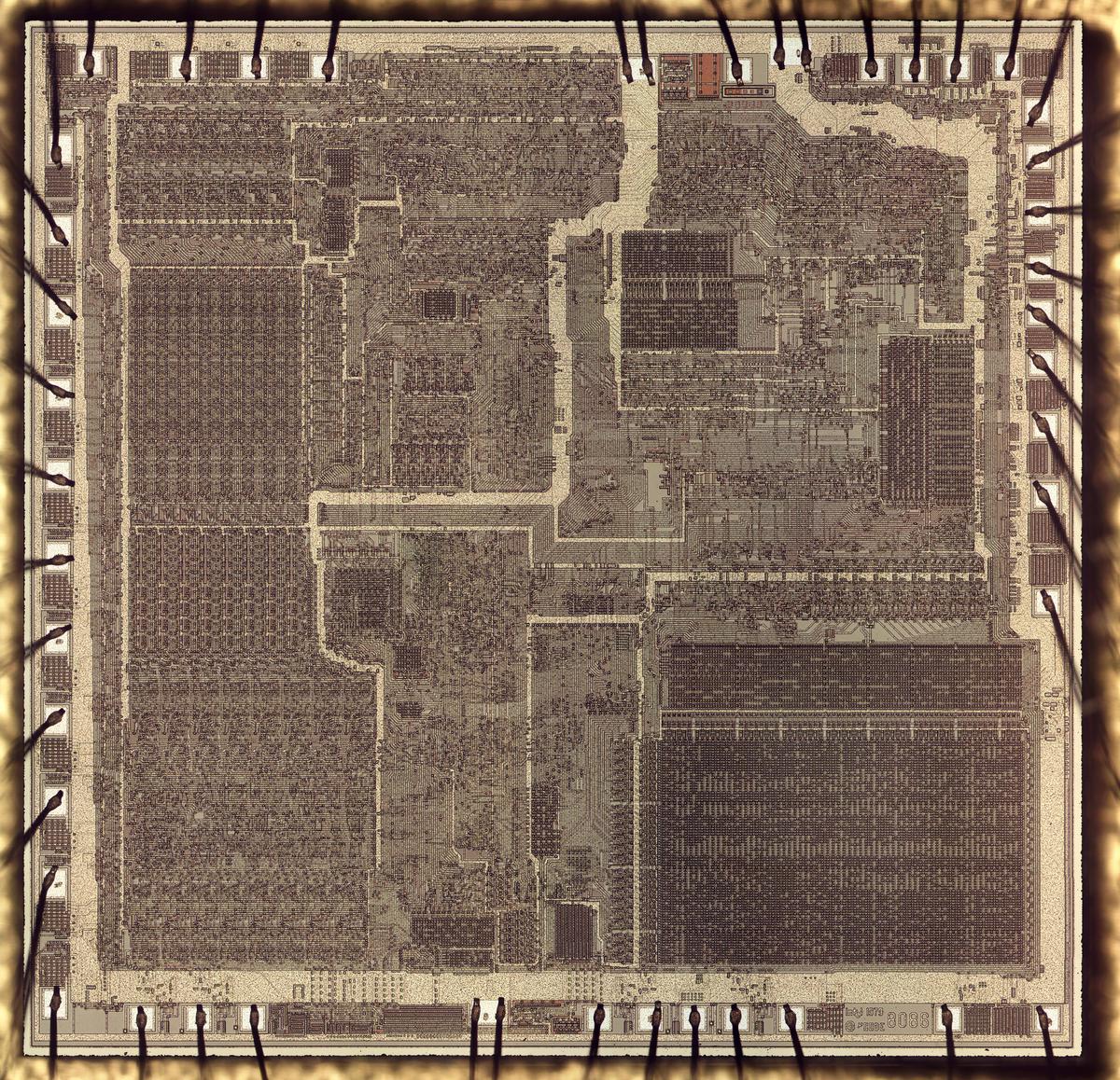
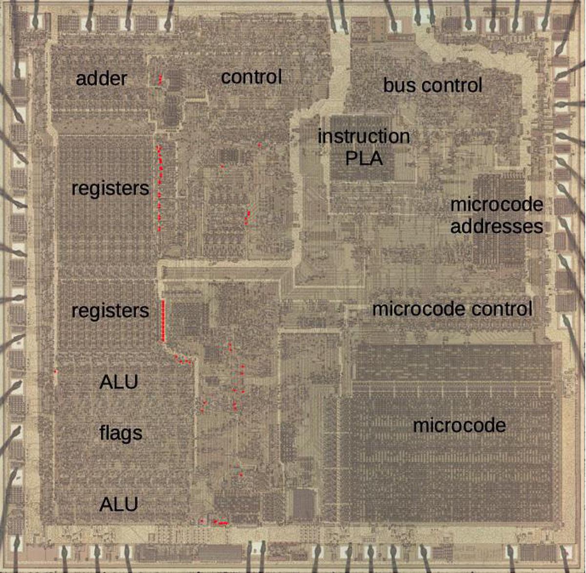
In total, the 8086 has 81 bootstrap drivers, mostly controlling the register file and the ALU (arithmetic-logic unit). The die photo below shows the location of the drivers, indicated with red dots. Most of them are in the center-left of the chip, between the registers and ALU on the left and the control circuitry in the center.
Conclusions
For the most part, the 8086 uses standard NMOS logic circuits. However, a few of its circuits are unusual, and the bootstrap driver is one of them. This driver is a tricky circuit, depending on some subtle characteristics of MOS transistors, so I hope my explanation made sense. This driver illustrates how Intel used complex, special-case circuitry when necessary to get as much performance from the chip as possible.
If you're interested in the 8086, I wrote about the 8086 die, its die shrink process and the 8086 registers earlier. I plan to write more about the 8086 so follow me on Twitter @kenshirriff or RSS for updates.
Notes and references
-
Intel used a "bootstrap load" circuit in the 4004 and 8008 processors. The bootstrap load has many similarities to the bootstrap driver, using capacitance to boost the output voltage. But it is a different circuit, used in a different role. The bootstrap load was designed for PMOS circuits to boost the voltage from a pull-up transistor, using explicit capacitors, built with a process invented by Federico Faggin. I wrote about the bootstrap load here. ↩
-
The only explanation of a bootstrap driver that I could find is in section 2.3.1 of DRAM Circuit Design: A Tutorial. The 8086 transistors with the gate wired to +5V puzzled me for the longest time. It seemed to me that this transistor would always be on, and thus had no function. However, the high voltage of the bootstrap driver gives it a function. I was randomly reading the DRAM book and suddenly recognized that one of the circuits in that book was similar to the mysterious 8086 circuit. ↩
-
The threshold voltage was considerably higher for older PMOS transistors. To get around this, old chips used considerably higher supply voltages, so "losing" the threshold voltage wasn't as much of a problem. For instance, the Intel 4004 used a 15-volt supply. ↩
-
The reason that MOSFETs are symmetrical in an integrated circuit and asymmetrical as physical components is that MOSFETs really have four terminals: source, gate, drain, and the substrate (the underlying silicon on which the transistor is constructed). In component MOSFETs, the substrate is internally connected to the source, so the transistor has three pins. However, the source-substrate connection creates a diode, making the component MOSFET asymmetrical. Four-terminal MOSFETs such as the 3N155 exist but are rare. The MOnSter 6502 made use of 4-terminal MOSFET modules to implement the 6502's pass transistors. ↩
-
The load transistor is a special type of transistor, a depletion transistor that is doped differently. The doping produces a negative threshold voltage, so the transistor remains on and provides a relatively constant current. See Wikipedia for more on depletion loads. ↩
-
The superbuffer has some similarity with a CMOS gate. Both use separate transistors to pull the signal high or low, with only one transistor on at a time. The difference is that CMOS uses a complementary transistor, i.e. PMOS, to pull the signal high. PMOS performs better in this role than NMOS. Moreover, a PMOS transistor is turned on by a 0 on the gate. This behavior eliminates the need for the inverter in a superbuffer. ↩
-
The 8086 processor also uses completely different charge pumps to create a negative voltage for a substrate bias. I discuss that use of charge pumps here. ↩
-
Why is it called a bootstrap driver? The term originates with footwear: boots often had boot straps on the top, physical straps to help pull the boots on. In the 1800s, the saying "No man can lift himself by his own boot straps" was used as a metaphor for the impossibility of improvement solely through one's own effort. (Pulling on the straps on your boots superficially seems like it should lift you off the ground, but is of course physically impossible.) By the mid-1940s, "bootstrap" was used in electronics to describe a circuit that started itself up through positive feedback, metaphorically pulling itself up by its bootstraps. The bootstrap driver continues this tradition, pulling itself up to a higher voltage. ↩
-
Some circuits in the 8086 use physical capacitors on the die, constructed from a metal layer over silicon. The substrate bias generators use relatively large capacitors. There are also some small capacitors that appear to be used for timing reasons. ↩
-
The exact voltage on the gate will depend on the relative capacitances of different parts of the circuit, but I'm ignoring these factors. The voltages that I show in the diagram are illustrations of the principle, not accurate values. ↩
-
Some of the 8086's bootstrap drivers pre-discharge when the clock is low and produce an output when the clock is high, while other drivers operate on the opposite clock phases. The ALU drivers in the die photo operate on the opposite phases, but I've labeled the diagram to match the previous discussion. ↩
11 comments:
This site is so nerdly. I just love it.
Even if I don't get all of it. Keep doing it.
I believe this is called a 'level restorer' in VLSI design.
It's always interesting to see what inventive ways early designers came up with. This all seems like forgotten knowledge because things are so much 'simplified' and 'abstracted away' nowadays, which are positive qualities needed to designing very complex things.
It's not unlike how modern software engineering works vs early assembly language, and the tricks (ab)used by the demoscene and Quake programmers.
https://authors.library.caltech.edu/26956/
Here is a link to the Hot Clock NMOS work from Caltech that used the bootstrapping idea in a different way.
You succeeded! Crystal clear explanation.
In the "Notes and references" section, #4 - I believe it is the Drain-Substrate interface which creates the diode, as the Source-Substrate interface has been shorted.
Great read, thanks for sharing.
Please do de same with RISC-V chip. /
For didatical pourpose....
TKS.
Great read! One slightly misleading comment: "However, the source-substrate connection creates a diode, making the component MOSFET asymmetrical.". IIRC, by default a four-terminal MOSFET has two back-to-back diodes between the source-substrate-drain (which block current in both directions). Connecting the substrate to the source shorts out one these MOSFETs, leaving just the one "body diode", hence the asymmetry. This then also allows conduction in one direction.
I've typed up some info on MOSFETs at https://blog.mbedded.ninja/electronics/components/transistors/mosfets/, I'll make sure to add this interesting effect soon.
They are hardly unique to 8086. Go get a 1980's circuit design textbook.
These articles are awesome!
Please continue!
Ahhhh.... such Nostalgia . . .
Thanks, Ken, and let me help you out with your last puzzle / (#2 on) . . .
I was a designer on the 8087 (the Numeric coprocessor for the 8086/88), and we used this driver there too... we referred to it as the "Peter Stoll" driver, as per this great designer whom we got it from . . .
This "NMOS process" you refer to actually had 4 types of transistors... you might be familiar with the standard "N" and "D" types, but we also had a "W" and an "L type. . .
The W type transistor was one with a Vthreshold of 0 . . . so in this implementation it served like a diode: when the upper gate of the last pair of xtors 'spiked' to the high voltage, this W xtor will cut off the path to the previous stage (normally there was an Inverter before these 3 xtors you've described), to not lose that high voltage . . .
Good luck ! and keep the fun comming . . .
Post a Comment