Texas Instruments introduced the first commercial single-chip computer in 1974, combining the CPU, RAM, ROM, and I/O into one chip. This family of 4-bit processors was called the TMS1000.1 A 4-bit processor now seems very limited, but it was a good match for calculators, where each decimal digit fit into four bits. This microcontroller was also used in hand-held games2 and simple control applications such as microwave ovens.3 Since its software was in ROM, the TMS1000 needed to be custom-manufactured for each application, but it was inexpensive and sold for $2-$4 in quantity. It became very popular and was said to be the best-selling "computer on a chip".

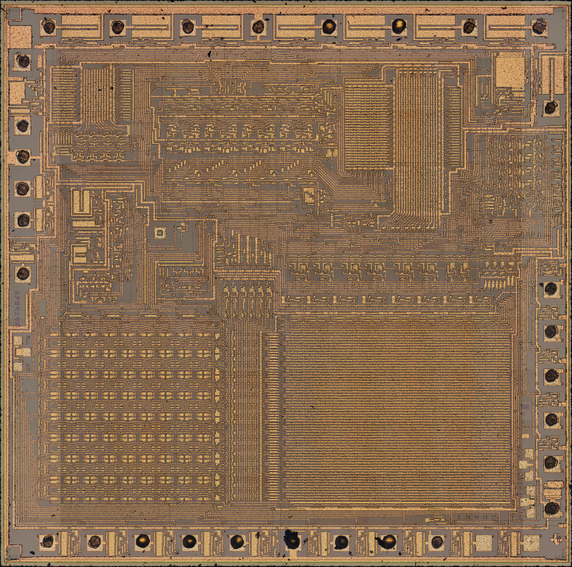
The die photo above shows the main functional blocks of the TMS1000. One thing that distinguishes the TMS1000 (and most microcontrollers) from regular processors is the "Harvard architecture", where code and data are stored and accessed separately. In the TMS1000, code and data even have different sizes: instructions were 8 bits and stored in a 1-kilobyte ROM, while data was 4 bits and stored in a 64×4 (256-bit) RAM.4 Since the space for RAM was limited, Texas Instruments developed new circuits for RAM. In this blog post, I look at how the TMS1000 and later TI chips implemented their on-chip RAM.
TMS1000 RAM
Dynamic RAM revolutionized memory storage in the early 1970s; its low cost and high density rapidly made magnetic core memory obsolete. Dynamic RAM uses a tiny capacitor to store each bit, with a 0 or 1 represented by a low or high voltage stored in the capacitor. The problem with dynamic RAM is that the charge leaks away after a few milliseconds, so the values need to be constantly refreshed by reading the data, amplifying the voltages, and storing the values back in the capacitors.5 Texas Instruments developed a new dynamic RAM circuit for the TMS1000 to avoid the complexity of an external refresh circuit. Instead, each memory cell uses a clock signal to refresh itself internally.
The diagram below zooms in on the TMS1000 die photo, showing the 16×16 grid of RAM storage cells. The inset at the right shows a single storage cell. This photo shows the chip's metal layer; the transistors are underneath.

The TMS1000 is constructed from a type of transistor called PMOS, shown below. At the bottom, two regions of silicon (red) are doped to make them conductive, forming the source and drain of the transistor. A metal strip in between forms the gate, separated from the silicon by a thin layer of insulating oxide. (These layers—Metal, Oxide, Semiconductor—give the MOS transistor its name.) The transistor can be considered a switch between the source and drain, controlled by the gate. The metal layer also provides the main wiring of the integrated circuit, although the silicon layer is also used for some wiring.

The diagram below shows a closeup of one bit of storage in the TMS1000. The first die photo shows the yellowish metal layer. The metal layer both connects the circuitry and forms the gates of the transistors. The second photo shows the die after the metal has been dissolved with acid to reveal the silicon underneath. The conductive doped silicon appears pinkish, while the transistors are yellow squares. The black spot in the lower left is a via connecting the silicon to the metal above. Since the photo is hard to interpret, I created the diagram at the right, clarifying the components. The five white squares are the transistors, between pink silicon regions. There are also two capacitors (labeled) created by overlapping the metal and silicon.

The schematic below corresponds to the above circuit, with the transistors in their approximate physical locations. To write a bit, the bit is placed on the data I/O line and the address line is activated.8 This turns on transistor Q4 and allows the bit to flow to point A, where it is maintained (temporarily) by the capacitor there. The bit can be read out the same way, by activating the address line. In a typical dynamic RAM chip, each cell consists of just this transistor and capacitor, but the TMS1000 uses the additional transistors to refresh the voltage on the capacitor.

The TMS1000 refresh circuit is driven by two clock signals, clock phase 1 (Φ1) and clock phase 5 (Φ5).7 Activating clock phase 5 turns on Q3 and allows the bit to flow to point C, the gate of transistor Q1. Large transistor Q1 is the key component of the refresh circuit, as it amplifies the signal C. Next, during clock phase 1, the amplified signal at B flows through Q2, restoring the original bit stored at A. This circuit is repeated 256 times for the 256 bits of RAM storage in the chip. These clock signals are activated at about 80 kilohertz, ensuring the bit is refreshed before it can drain away.
The move to CMOS
CMOS (Complementary MOS) is a type of circuitry that combines NMOS and PMOS transistors to reduce power consumption. In 1978, TI began building CMOS calculator chips, starting with the TP0310 and TP0320 chips.6 These chips were used in calculators such as the TI-30-II (below), TI-35, and TI-50. The switch to CMOS coincided with TI's switch from power-hungry LED or vacuum fluorescent displays (VFD) to low-power LCD (details). These improvements led to better battery life. TI also used CMOS to implement "Constant Memory™", preserving calculator data even when the calculator was off; CMOS's low power consumption meant that the memory could be continuously powered without draining the battery.

CMOS has a long history, starting with its invention in 1963. RCA did a lot of early development of CMOS, introducing the 4000-series of integrated circuits in 1968 and the first CMOS processor, the RCA 1802, in 1974. RCA was unfortunately a decade too early for market success with CMOS; although CMOS's lower power consumption made it useful for niche aerospace markets, NMOS processors dominated the microprocessor industry. Eventually, however, mainstream microprocessors switched to CMOS with the Intel 80386 in 1985 and Motorola's 68030 in 1987, and CMOS is the dominant technology today.
TI's move from metal-gate PMOS to CMOS in 1978 is unusual. Other manufacturers (such as Intel) switched from metal-gate transistors to the much superior silicon-gate transistors around 1971, and then moved from PMOS to NMOS around 1974. It's unclear why Texas Instruments continued using inferior metal-gate PMOS circuitry for several years; perhaps calculators didn't need the improved performance so it wasn't cost-effective to switch. But then Texas Instruments skipped over the NMOS generation entirely, jumping to CMOS a decade before the mainstream microprocessor industry. This decision is easier to justify, since low-power CMOS was a clear advantage for battery-powered calculators. Curiously, TI continued to use inferior metal-gate transistors, even after moving to CMOS.
This history illustrates that technological progress isn't a straightforward path with new and improved technologies replacing older technologies. Instead, a new technology like CMOS may take years to catch on, becoming successful in particular markets but being not making headway in other markets until economic factors and engineering tradeoffs changed.
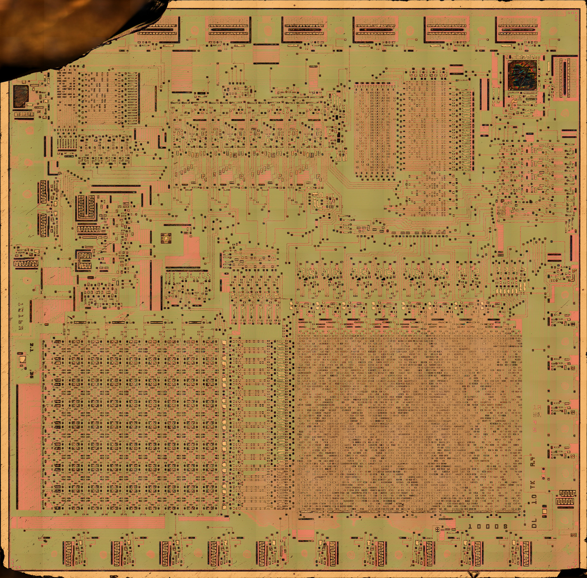
Getting back to the TP0320, the die photo below shows the TP0320 die, zooming in on the RAM array. This 32×24 array holds 768 bits, a significant upgrade from the TMS1000. The closeup at the right zooms in on a single bit. The bit cell has a different layout from the TMS1000 RAM. The design switched from dynamic RAM to static RAM, eliminating the capacitors and the need for refresh. In this section, I'll explain how this RAM cell is implemented.

The diagram below shows how two inverters can be connected in a loop to store either a 0 or a 1. If the upper signal is 1, the inverter on the right outputs a 0 on the bottom, and the inverter on the left outputs a 1 at the top, reinforcing the original signal. Alternatively, the top signal can be a 0 as shown on the righ. The key difference between this static circuit and the previous dynamic circuit is that the static circuit will hold a bit for an arbitrarily long time. The bit won't leak out of a capacitor as in a dynamic RAM, so refresh is not needed.

To make a usable storage cell, an addressing mechanism is added to the inverter circuit above. When the address select line is activated, the transistors connect the inverters to the data lines. For a read, the value of the cell is read from the data line. For a write, the desired bit and its complement are applied to the data lines, overpowering the value stored in the inverters and switching them to the new bit value. This type of storage cell is used to implement registers in many processors, including the Zilog Z80 and the Intel 8085.

The diagram below shows how a CMOS inverter is constructed from two transistors. The upper transistor is a PMOS transistor, while the lower transistor is an NMOS transistor. With a 0 input, the PMOS transistor turns on, connecting the output to the positive voltage (1). With a 1 input, the NMOS transistor turns on, connecting the output to ground (0). Thus, the output is the opposite of the input, as you'd expect from an inverter.

Putting this all together yields the schematic below. Transistors Q1 and Q3 implement one inverter, while transistors Q2 and Q4 implement the second inverter. Transistors Q5 and Q6 select the cell based on the address. The transistors are arranged on the schematic to match their physical locations.

The die photos below show how the storage cell is implemented in the TP0320 processor. The first photo shows three vertical metal traces that wire the cell together. In the second photo, the metal was removed with acid to reveal the silicon underneath. The upper section holds the PMOS transistors (Q1 and Q2) while the lower section holds the NMOS transistors (Q3 to Q6). The transistors appear as whitish rectangles, while the doped silicon appears as greenish or reddish lines. The black spots are vias connecting the silicon to the metal above. The diagram can be compared with the schematic above.

The photo below zooms out a bit to show how the NMOS and PMOS transistors are arranged. Note the "P ring" that surrounds the NMOS transistors. This forms a tub of P-type silicon that holds the NMOS transistors. (This P ring is the horizontal green line below Q2 in the die photo above.) The chip contains many of these tubs, separating the PMOS and NMOS transistors.

TP0456
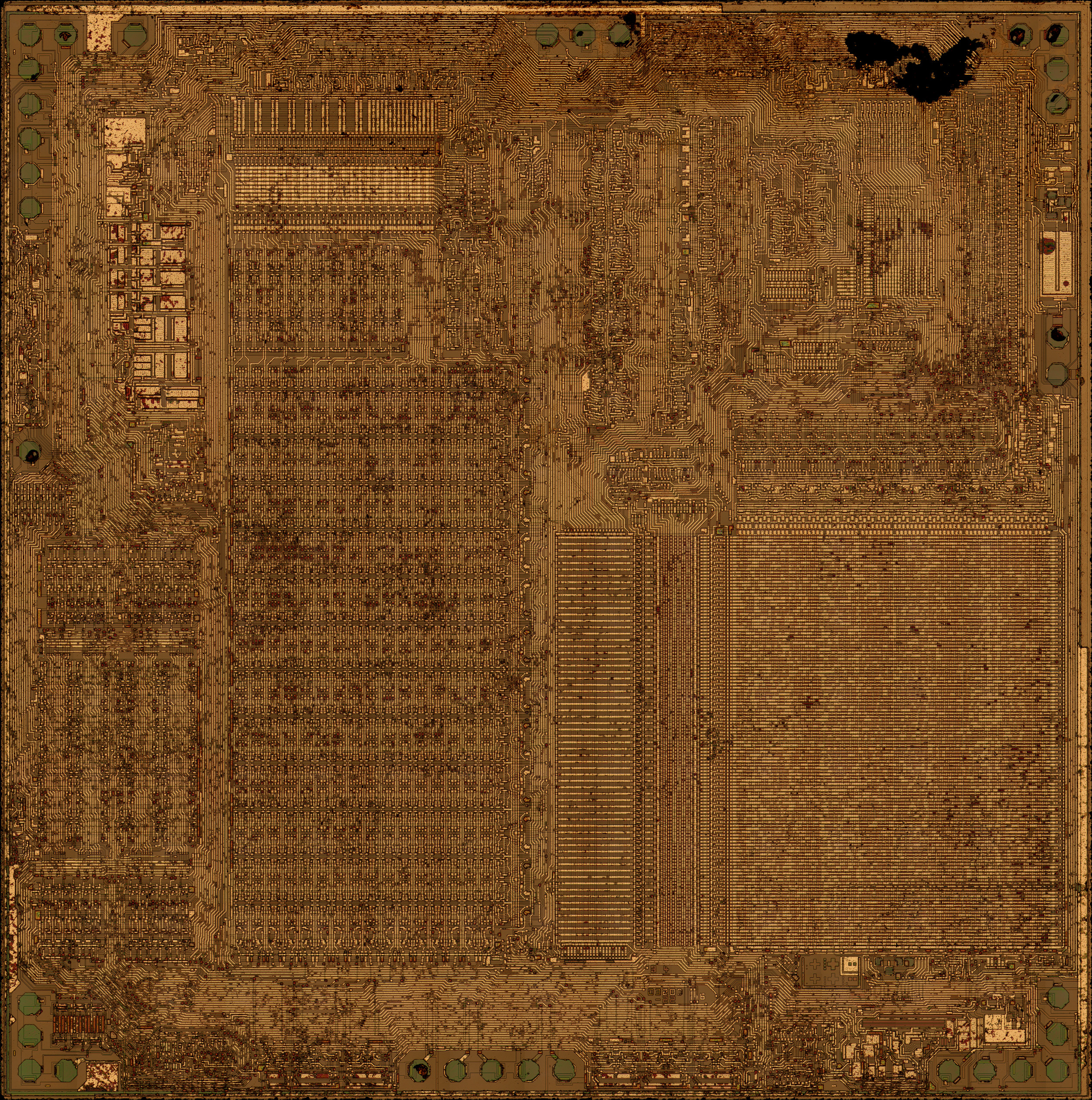
In 1981, Texas Instruments introduced a more powerful architecture, the TP0455, followed shortlly by the TP0456. The TP0456 chip was used in calculators such as the TI-55-II scientific calculator, TI-35, and TI-60, as well as educational toys such as Little Professor and Spelling B.

The die photo below shows the TP0456. The RAM array is in the lower-left corner of the die photo below, while the ROM is in the lower-right. The TP0456's RAM array is 32 cells wide and 16 cells tall, providing 512 bits of storage, less than the 768 bits of the TP0320.

The TP0456 uses almost the same static cell structure as the earlier CMOS chips, but the layout was changed slightly. In particular, the select line runs between the two inverter lines, rather than on the side. I don't know why they made this change, as it doesn't appear to change the density. The static RAM circuit is same as the TP0320 described earlier, so I won't discuss it here.

Conclusion
While RAM storage may seem trivial, early microcontrollers required new ways to fit storage into the limited space on a die. Even just 256 bits took up a substantial fraction of the chip. Texas Instruments developed new dynamic RAM circuits for the TMS1000 microcontroller, followed by a completely different static circuit when they switched to CMOS microcontrollers.
Decades later, microcontrollers still have limited memory capacity. The Arduino Uno, for example, has 32 kilobytes of flash for program storage and 2 kilobytes of RAM. Modern high-end microcontrollers can have megabytes for program storage and hundreds of kilobytes of RAM, but this is still orders of magnitude less than a typical microcomputer. The constraints of fitting everything onto a single chip still limit capacity and still require novel solutions, just as in the TMS1000.
I announce my latest blog posts on Twitter, so follow me at kenshirriff. I also have an RSS feed. Thanks to Joerg Woerner at Datamath for suggesting this topic and thanks to Sean Riddle for die photos.
Notes and references
-
Texas Instruments is considered the inventor of the microcontroller for developing the TMS0100 (different from the TMS1000) in 1971. While the TMS0100 has the characteristics of a microcontroller, it was marketed as a "calculator-on-a-chip". The TMS1000, however, was marketed as a "single-chip computer" for both calculator-type applications and small to medium control applications. ↩
-
The architecture of the TMS1000 is rather unusual due to its roots as a calculator chip. It has just four input lines, designed to be connected to a grid of buttons. The outputs are also unusual: it has 8 "O" output lines, but these are not individually controllable. Instead, a 5-bit value is converted to the eight outputs by a customizable PLA decoder. The motivation behind this is to drive a 7-segment display. The microcontroller also has 11 "R" outputs, which are typically used to multiplex the LED display and to scan the keyboard. Another curious feature of the TMS1000 is that the instruction set was somewhat customizable.
In comparison, Intel's microcontrollers such as the popular 8048 (1976) and 8051 (1980) were much more like standard 8-bit microprocessors. Unlike the TMS1000, the Intel microcontrollers had familiar features such as an 8-bit CPU, 8-bit I/O ports, interrupts, a stack, and a fixed instruction set with Boolean operations (AND, OR, XOR) and shifts. Looking at the TMS1000 instruction set, it seems slightly alien, while the 8048's instruction set is similar to microprocessors of the time. ↩
-
Detailed information on the TMS1000 is in the TMS1000 manual. ↩
-
Dynamic RAM is sometimes used for register storage in a processor, such as the Intel 8008, although static RAM is more common since it doesn't require refreshing. ↩
-
The Datamath Calculator Museum has tons of information on Texas Instruments calculators. The list of ICs is particularly relevant. ↩
-
The TMS1000 is implemented with complex logic circuitry, using a five-phase clock. The TMS1000 uses a mixture of depletion loads, gated loads, or precharge logic, for power savings. I'm not sure why the TMS1000 uses a five-phase clock. Four-phase logic was a logic design methodology at the time, but the TMS1000 circuitry doesn't appear to use four-phase principles. Among other things, the TMS1000 phases are irregular and Φ4 pulses twice per cycle. ↩
-
TI's Random access memory cell patent (1974) describes the memory cell used in the TMS1000. The layout in the patent is similar but not identical to the actual layout. Transistor Q5 appears in the circuit but not the patent. It pulls point B to 0 when clock phase 5 is active, making sure that a 0 bit at C is restored to a stronger 0 bit.
 Diagram of a dynamic RAM cell, based on the Random Access Memory Cell Patent.
While most patents don't provide much useful information, Texas Instruments' calculator patents are unusually detailed and informative, providing schematics, source code, and clear explanations; they seem like they were written by engineers. (I feel that I should give TI credit for the quality of their patents.) ↩

15 comments:
I did the code for a c64 mouse using a 4bit micro from Toshiba. TCLS42. Was fun as i was only 18 at the time, around 85
Nice. I wonder why they used the complicated DRAM cell instead of SRAM. It does not appear to save any real estate. Or does it? Does it save power then?
The TMS1000/1100 series 4-bit uPs were the start of my professional career as a programmer, working at GEC Telecoms in the UK on electronic (rather than simply electro-mechanical) telephone designs to work with small PBX systems.
All our coding was done on Cipher CP/M machines, in assembler. Masks were generated from our tapes sent to TI Bedford, taking around 12-16 weeks to fab. You really *couldn't* afford to have any bugs in your code...
It gave me a greater appreciation of economy of coding and documentation in the code, and *always* testing results rather than just assume success ("Happy Path" coding).
As a precursor, my final year B.Sc. project, completed before starting at GEC, was the implementation of a microstrip scaling algorithm by large, floating point matrix multiplication - implemented on a TI-59 programmable calculator: restricted memory and register availability was directly applicable to what I later ended up doing on the phone designs - a program coded in just 76 nibbles, using 14 nibbles of RAM for the entire button control panel and call management!
This is a great article, and much enjoyed. 10/10, Ken!
s/caell/cell/
Hi Ken,
Thank you for another brilliant write-up. I read all of them as detective stories and take my hat off to your knowledge and ease you are explaining it to us.
It seems that density of actual transistors, which are surprisingly small, in each RAM cell is quite low. Is there any particular reason for it?
Thank you
KR
Pavel
> Nice. I wonder why they used the complicated DRAM cell instead of SRAM. It does not appear to save any real estate. Or does it? Does it save power then?
Without complementary transistors, the passive pull-ups for the inverters would draw too much power compared to a dynamic memory cells which spend considerable time idle.
Are the two refresh signals 180 degrees out of phase with each other? I was reading and re-reading the paragraph describing how it works, and wondering why you have Clock 1 on two seperate lines, but the patent application made it more clear why was was. But I'm still confused. Just a dumb CS major. *grin*
But, very interesting anyway since I've worked with ASIC design groups for the past 16 years, so I've picked up some of this over time. Very little, and these posts help me learn more.
Pane: the density is pretty good for metal-gate circuitry. Since there's just one layer for wiring (no polysilicon), chips often use most of the area to get signals to the transistors, and the transistor density is very bad. So I think they did a good job with the memory cell given the constraints.
John S: According to the patent, phase 1 is active for two clock intervals, then phase 5 is active for 1 clock interval, then they are both inactive for 3 clock intervals. They don't overlap, but since they are different widths they aren't really 180 degrees out of phase.
Others: thanks for the comments!
Thank you for these posts as well. This post and the previous post form some great foundations as to how RAM works and I have found them very informative.
You regularly read that chips have to be redesigned when processes change. And as a software person, I am wont to say: "Why can't they just take the masks and make them a little smaller? Or when going from NMOS to CMOS, why wouldn't they put the same transistors in the same places?".
The progression of RAM technology is a great example of why that is naïve. Thank you for explaining so clearly. When dealing with software we work at a much higher abstraction layer, but it really helps to understand how things work and why we can or cannot make these abstractions.
nice post.
Professor Prem raj Pushpakaran writes -- 2023 marks the birth centenary year of Jack S. Kilby!!!
https://worldarchitecture.org/profiles/gfhvm/prof-prem-raj-pushpakaran-profile-page.html
Hey there Ken! you commented on a hacker news post almost 10 years ago:
"That's kind of how the TMS1000 microcontroller (used in the Speak n Spell) works. Instead of incrementing the program counter on each instruction (like every normal processor), they saved a few gates by using a linear feedback shift register. The result is the program counter goes through a pseudo-random but predictable sequence. So they just program the code into the ROM in the same sequence and everything works just fine. (Some day I'll write a blog post about this, since it's interesting to look at the silicon that does this.)"
any chance you are still going to write up some info on this?
thanks!
Hello I am trying to serv an old tuner Quad34 and I found a strange circuit TMS1000NLC that was broken. I have tried to understand what it is doing there in the tuner from the 70's. Now I think I understand and I found your interesting blog ( I think for us electro-people it is very interesting). So I have a short question if you have the time to answer? Is it possible to reengeneer that ic, to read a working one and then program a new empty one. What I understand it is ipossible!
Chris from Sweden
Hi Ken,
As per Note #8 it seams there are at least two patents - one you mentioned 3,876,993 and also 3,955,181 related to memory refresh and the second one is closer to your physical observations and includes missing transistor Q5. Despite lower number of the patent the filing date is later (Nov. 74 for 3,955,181 compared to March 74 for 3,876,993). Something must went wrong with the original design.
KR
P
Post a Comment