IBM and its large mainframe computers ruled the computer industry for decades. But during the 1980s, mainframes faced increasing competition from microprocessors, workstations, and super-minicomputers. To meet this challenge, IBM pushed technology to the limit to create the ES/9000 in 1991, a family of powerful mainframes with a price tag to match, from $70,500 up to $22 million. The processor of the ES/9000 wasn't a single chip, but a metal and ceramic package called a Thermal Conduction Module (TCM) that held 121 chips. Recently, Dave Jones of EEVBlog created a popular teardown video of a TCM, showing its complex construction. After disassembling the module, he kindly sent me some of these cutting-edge chips to analyze. In this blog post, I examine the circuitry inside one of these logic chips from the ES/9000.
The ES/9000
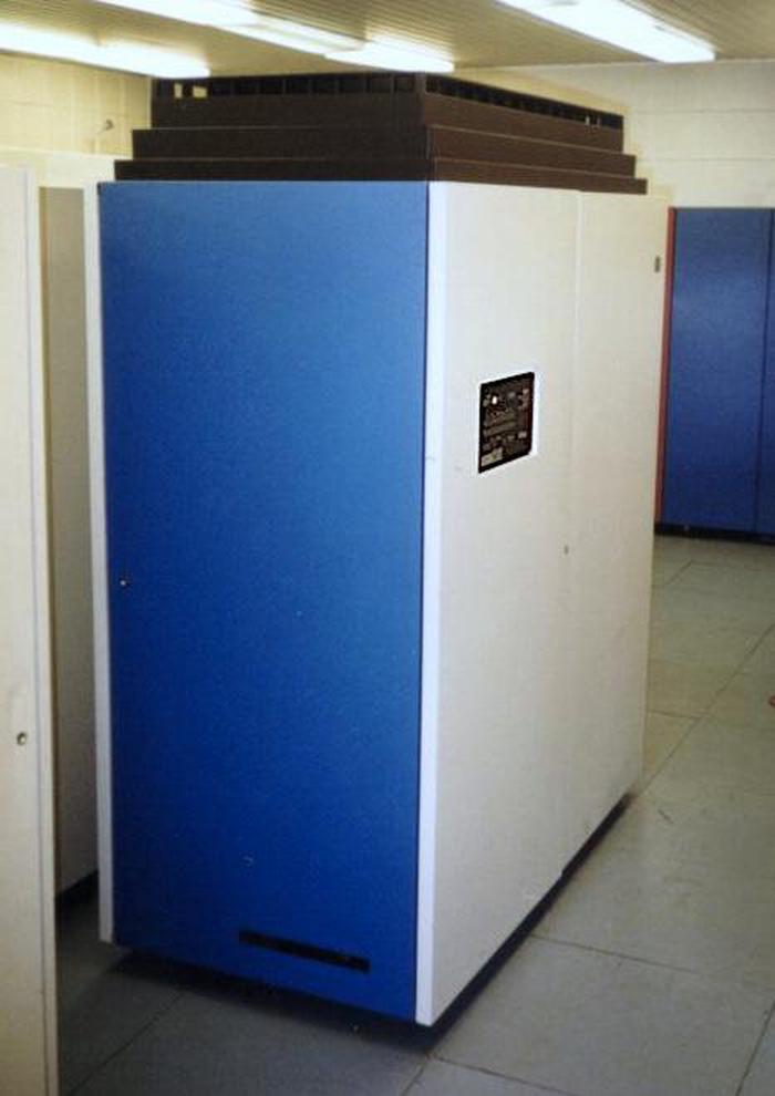
The ES/9000 family of computers consisted of three lines with performance spanning two orders of magnitude: small entry-level systems for an office, mid-range air-cooled systems (below), and high-end water-cooled systems that could fill a room. The technology of the ES/9000 was very advanced for its time in many ways. Along with the ceramic thermal conduction modules, IBM created new high-speed integrated circuits with state-of-the-art transistors. At the system level, IBM introduced new operating systems as well as ESCON (Enterprise Systems Connection), a high-speed fiber-optic connection between the mainframe and peripherals. An optional cryptographic feature provided high-speed encryption in tamper-resistant hardware. Even the power supplies were innovative; the water-cooled power supplies could be swapped while the computer was running. The innovations of the ES/9000 generated numerous journal articles and patents.1
In this article, I'm focusing on the mid-range systems, known as the 9121 processors.2 This system (above) was packaged in a drab frame the size of a large refrigerator.3 It used 7.4 KVA of power, occupied 14.7 square feet of floor space, and weighed 2000 pounds. It could hold up to 1 gigabyte of memory, a large capacity at a time when personal computers typically had 1 to 4 megabytes of RAM. A typical 9121 system cost $1.5 million and had about twice the performance of a contemporary Intel 80486 computer that cost $10,000. This is a bit of an apples-and-oranges comparison, since the mainframe gave you high-speed I/O channels, fast memory access, and an advanced operating system, but it shows the dramatic price/performance advantage of microprocessors.
The TCM (Thermal Conduction Module)
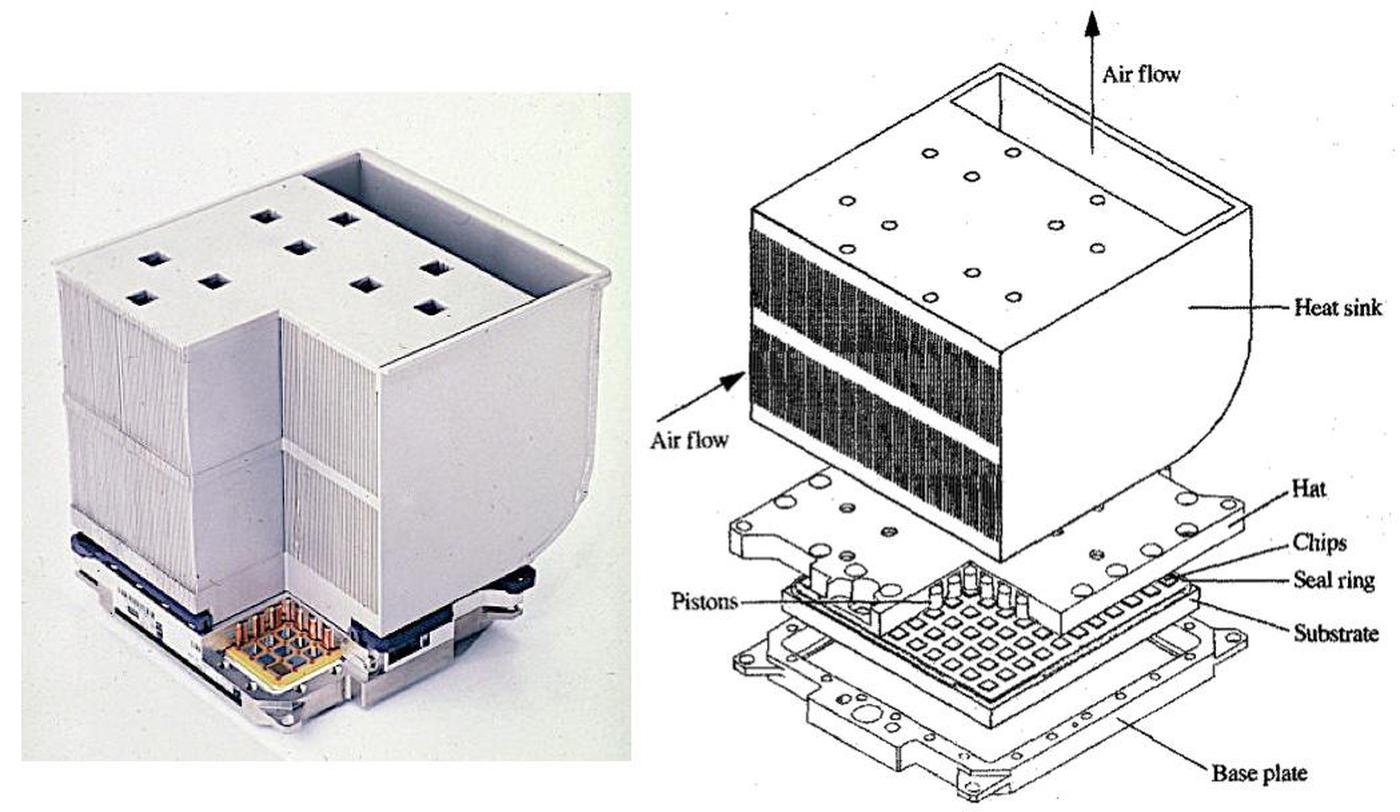
One of the most interesting features of the ES/9000 was the Thermal Conduction Module (TCM) that held the integrated circuits. The high-performance bipolar chips generated a lot of heat, so IBM developed new cooling mechanisms so this computer could function without water cooling. The cut-away photo below shows a TCM with its large heat sink attached. At the bottom, some of the integrated circuit dies are visible along with the copper cooling pistons. The computer's main circuitry consists of five different TCMs.4
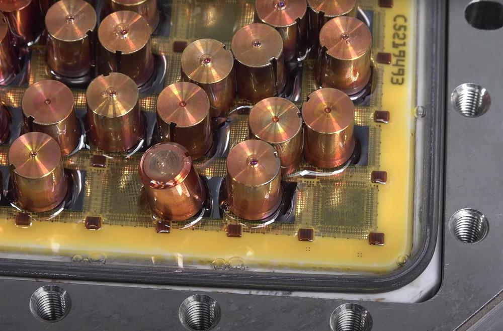
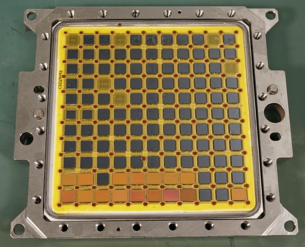
The TCM is surprisingly small, 5 inches (127.5mm) on a side, yet it holds 121 integrated circuits. Each integrated circuit has a spring-loaded copper piston on it to remove the heat. These pistons transfer the heat into the TCM's metal case, where the heat passes into the heat sink and then the air flow. The pistons are precision-machined to maximize contact and thus heat transfer. The module is filled with oil (visible below), which also increases heat transfer. The design of the TCM allows it to dissipate 600 watts of heat—imagine holding six 100-watt light bulbs in your hand.
The integrated circuits in the TCM are not packaged like regular integrated circuits, but consist of a silicon die soldered upside-down to the ceramic substrate, flip-chip style. This ceramic substrate is an incredible feat of engineering. It's essentially a printed-circuit board made out of ceramic, with 63 layers of wiring inside. It has over 80,000 connections on the top to the integrated circuits, 2 million vias, 400 meters of internal wiring, and 2772 pins on the bottom.
The manufacturing process for the ceramic substrate was very complex. Each ceramic sheet, the thickness of two sheets of paper (0.2mm), has tens of thousands of via holes punched in it. Next, the wiring was applied in the form of a molybdenum metal paste, forming wires just 100µm wide. The stack of 63 sheets was then laminated under heat and pressure. Next, the stack was sintered at 600°C to decompose the polymer binder, followed by hydrogen treatment at 1560°C for densification. During this process, the substrate shrank by 17%, but the millions of vias must remain aligned. After trimming and polishing, two layers of thin-film wiring were placed on top of the substrate. (The thin-film wiring allowed wiring changes to be made to the module for bug fixes.)5 Finally, the module was protected with a layer of polyimide film, with thousands of openings burned in it with a laser for the chip's connections.
The bipolar logic chip
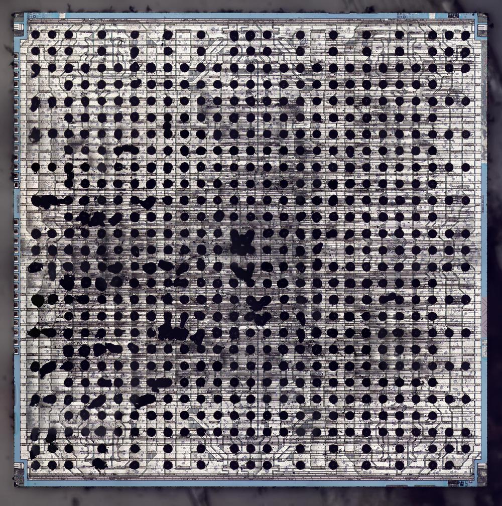
Most of the chips on the TCM are bipolar logic chips; these are the square black chips in the previous photo. The die photo below shows one of these logic chips, 6.5mm on a side.8 This chip has an unusual appearance because it was connected directly to the substrate instead of the typical approach of putting pads around the perimeter with bond wires attached. The black circles are the 549 solder balls in a 27×27 grid that connect the chip to the substrate. Of these connections, 228 of these are used for signals, while 321 are used for power. The chip is covered with metal conductors that connect the solder balls to the circuitry underneath.
The chip is built from a type of transistor called the bipolar transistor, an older type of transistor than the MOS transistors in modern processors. The transistors in this chip used a cutting-edge design with a complex internal structure.6 IBM used bipolar transistors because they provided higher performance at the time, but they had the disadvantages of using higher power and taking up more area on a chip. (This is why the chip needed 321 connections for power and why the ES/9000 required multi-chip modules with a complex cooling system.) The chip contains approximately 85,000 transistors, 40,000 resistors, 10,000 capacitors, and 1000 Schottky diodes. While this may seem like a large number, contemporary CMOS microprocessors (such as the Intel 486) contained over a million transistors, illustrating the much higher density of MOS transistors.7
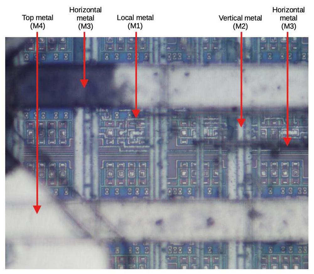
As shown in the closeup photo below, the chip has four layers of metal wiring on top of the silicon, a lot of layers for the time. The metal layer on top of the chip (called M4) provides power and signal distribution from the solder bumps. Underneath, layer M3 provides horizontal wiring: thick lines to distribute power across the chip and thin lines for signals. Layer M2 provides vertical wiring for both power and signals. The bottom layer (M1) implements the local wiring of the gate circuitry, connecting the transistors and resistors together. The narrowest metal lines are 1.6µm wide. Power distribution uses a hierarchy: the numerous solder balls feed power into the very wide power lines in the top metal layer. These are interconnected with the wide horizontal lines, which connect to the thinner vertical lines, which connect to the circuitry. This hierarchy ensures that voltage drop is minimized across the chip, while providing the multi-amp current it requires.
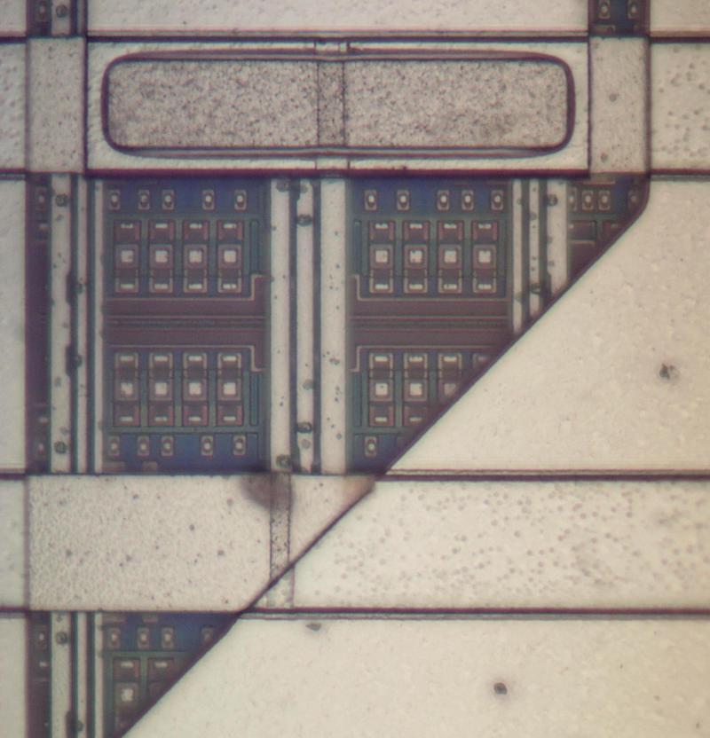
The architecture of the chip is IBM's "master slice" approach, building the chip from a gate array of identical cells. To avoid the expense of creating fully-custom chips, IBM built the various logic chips from a common grid of cells that was customized by the wiring on top. In the photo above, you can see some of these cells underneath the metal. The master cell approach has the disadvantage of being less dense than a custom chip. It turns out that roughly half of the cells in each logic chip went unused because the number of I/O pins on the chip was too small.12 You can see that most of the cells are unused in the photo above; while the transistors and resistors are present, they aren't connected to anything.
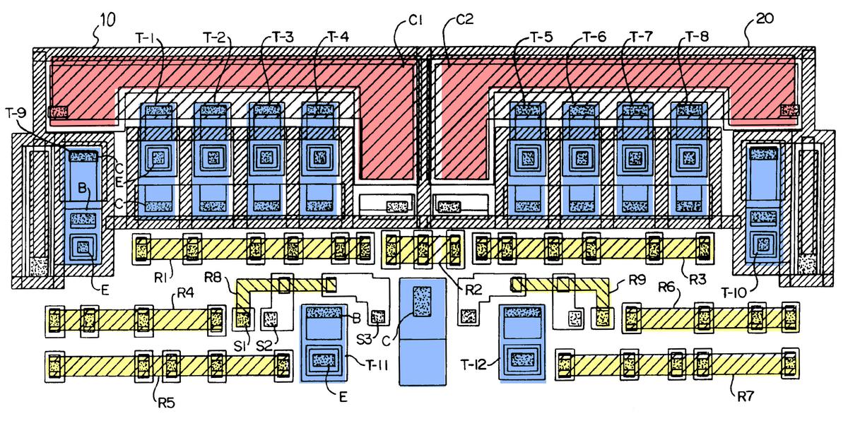
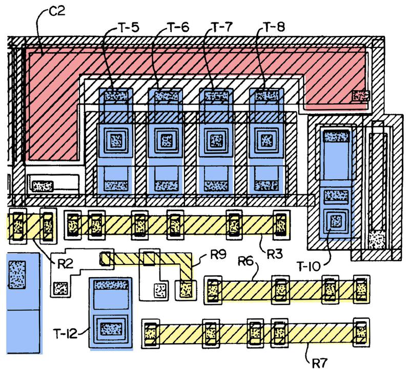
The chip contains 5240 cells, capable of implementing 2620 DCS logic gates. The structure of a cell is shown below. The cells are very flexible: each cell can implement one gate in the ECL (Emitter-Coupled Logic) family,9 two gates in the NTL (Non-Threshold Logic) family,10 or half a gate in the DCS (Differential Current Switch) family (which this chip uses). The key components are the transistors, which I've colored blue. The resistors are colored yellow.11 At the top are two large capacitors (red). The capacitors are unused in this DCS circuitry, but can be used to speed up ECL gates.
The image below shows six of the chip's 5240 cells after removing the metal layers from the chip. You can see how the layout matches the diagram above. (The cells in the middle are upside down.)
The logic chips are fabricated with a special technique that allows hundreds of different types of logic chips to be produced from a single set of masks. The transistors and other components in the silicon "master slice" are constructed using masks and photolithography as in most integrated circuits. However, the metal layers are patterned using direct-write electron beam lithography, rather than masks. This electron beam is steered to "write" the desired metal layer patterns on the die to produce the desired type of chip. In other words, the basic pattern of the chip is created using masks, but then the different chip types are manufactured directly from the design files, providing flexibility.
The photo below shows the entire die after dissolving the metal layers. This image shows the grid of cells, as well as three vertical rows holding 360 I/O cells.13 The grid pattern is most clear in the upper-right corner, where I sanded the die down. (Due to the difficulty of removing four layers of metal as well as layers of silicon nitride, I couldn't get the die as clean as I like.)
Differential Current Switch logic (DCS)
The chip is built with an uncommon logic family called DCS (Differential Current Switch).15 As the name suggests, DCS operates on differential signals: each input signal is expressed by two wires carrying both the signal and its complement. The voltage difference between the two wires represents a 0 or 1. Thus, a three-input logic gate will have six input wires, as well as two output wires.
Most logic families implement a NAND or NOR gate as their basic gate.
The basic DCS gate, however, is the SELECT operation:
it outputs either input A or input B, selected by the S input.
In other words, SELECT implements the function if S then A else B, or in Boolean logic, SA+S'B.
The SELECT operation is surprisingly flexible; with appropriate inputs, it can implement AND, XOR, or even a latch.14
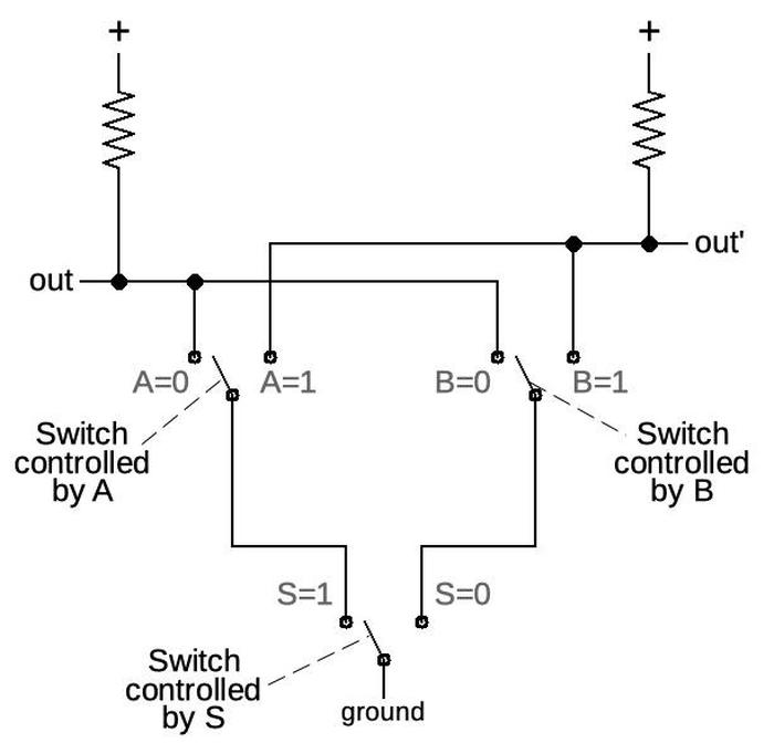
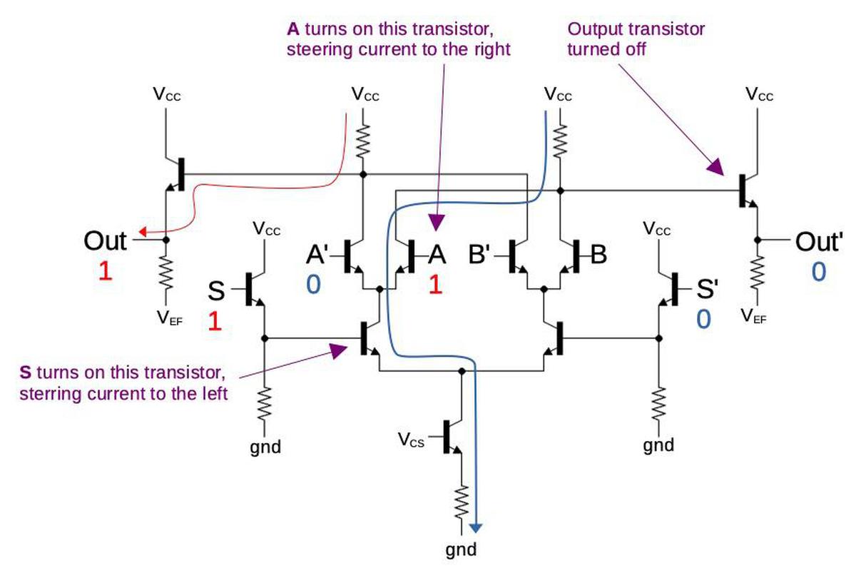
A SELECT gate is shown below at the conceptual level. Three toggle switches are controlled by the S, A, and B inputs. These switches will pull one output to ground, while the other output will be pulled high by a resistor. Starting at the bottom, the S switch will direct the ground current to either the "A" side or the "B" side. With the switches in the indicated positions, the output will be pulled to ground, while the complemented output remains high. But if input A is set to 1, the output levels reverse, with the output pulled high. Now, suppose input S is set to 0, so the current is directed to the B side. In this case, the output is controlled by switch B. You can verify that the output matches A if S is 1 and matches B if S is 0. In other words, the circuit selects between inputs A and B, depending on the value of S. Note that this circuit generates differential outputs: both the output and its complement.
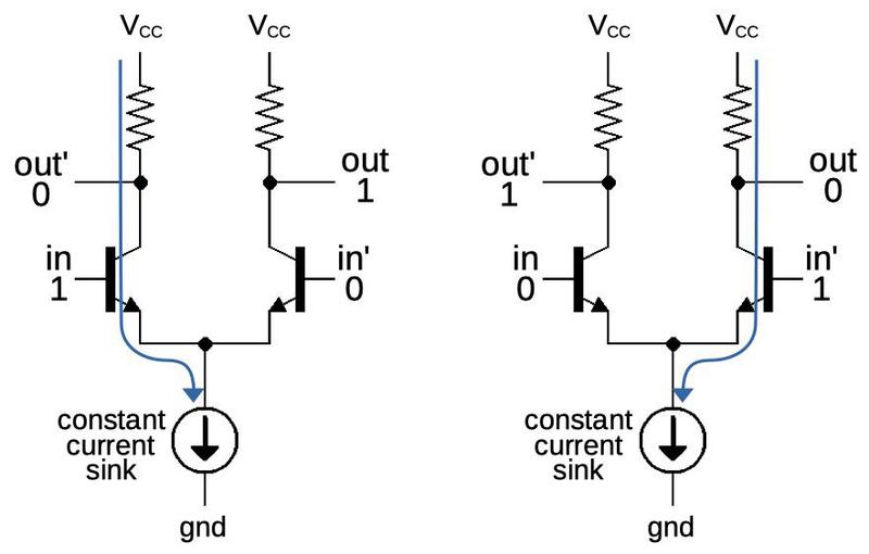
Next, I'll describe how the current switch is implemented with a pair of transistors. At the bottom, a current sink generates a fixed current, which can be switched to either the left side or the right side of the circuit. The idea is that the transistor with a higher input voltage will direct the current to that side, pulling that output low. Thus, the circuit acts like a toggle switch. An important feature of the circuit is that it provides a high degree of amplification: a slight difference in voltages is enough to switch most of the current to one side. (This circuit is essentially the same as the differential amplifier used in an op-amp.) As a result, a voltage swing of just 200 millivolts is enough to distinguish a logical 0 and 1, reducing power consumption. Another important feature of this circuit is that it is activated by the difference between the input voltages, so it is relatively insensitive to electrical noise. In other words, a voltage fluctuation that affects both inputs will cancel out, rather than causing an erroneous 0 or 1.
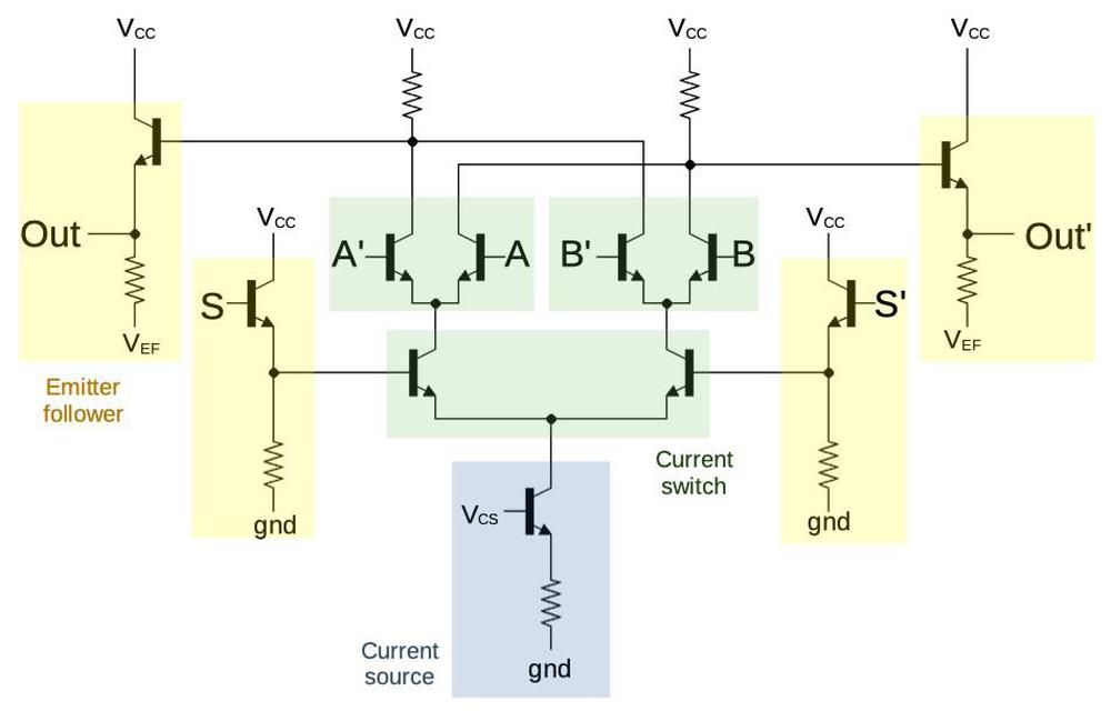
The schematic below shows the implementation of a DCS gate. The three green boxes are current switches, using transistor pairs as described above. The yellow boxes are buffer circuits, called emitter followers. Two emitter followers buffer the outputs, while two more are used on the select inputs. Finally, the blue box is the current sink circuit, providing the fixed current that gets switched by the circuit.
The diagram below shows this circuit in action. Starting at the bottom, the S input switches the current to the left. The A input then switches the current to the right. This current pulls the complemented output low, while the pull-up resistor pulls the output high. Note that a 0 input on A would switch the current to the other side, and thus switch the output. The B input has no effect since the current bypasses the B side of the circuit. Pulling the S input low, however, would switch the current to the B side, causing the B input to control the output. Thus, this circuit implements the SELECT operation.
Reverse-engineering a DCS gate
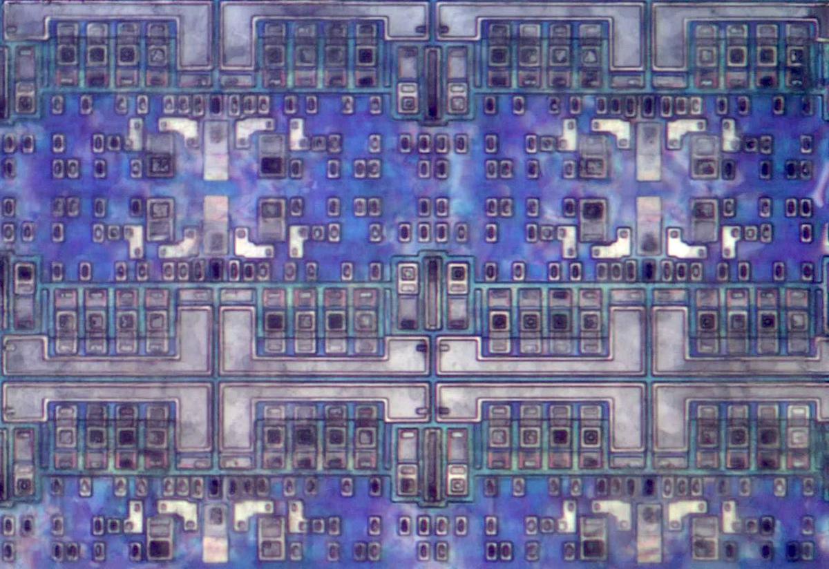
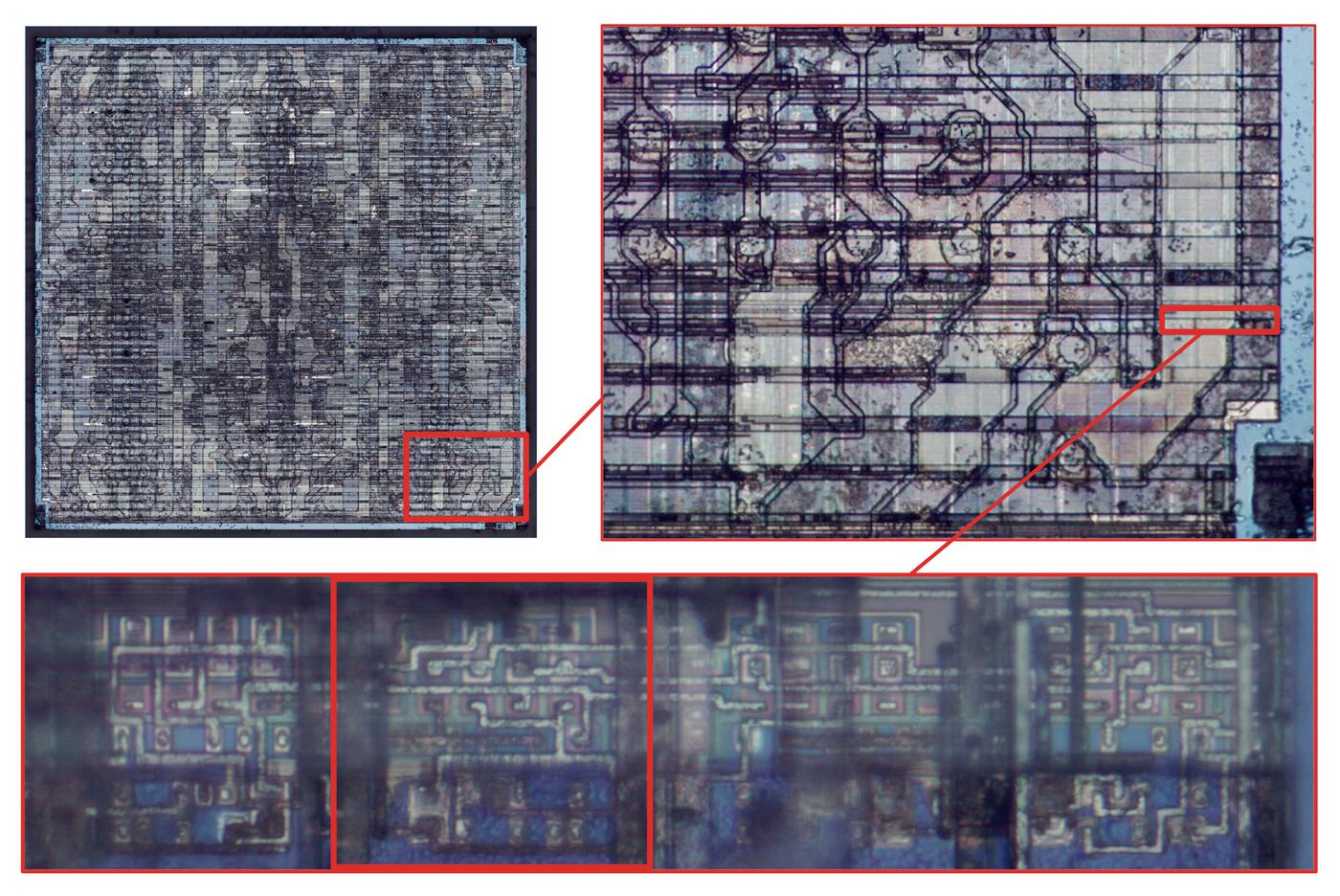
In this section, I'll look at how a SELECT gate is implemented on the chip. The diagram below zooms in on a corner of the die, and then zooms again on one logic gate, the rectangle at the bottom. As you can see, each logic gate is very small on the die. Because this gate is at the edge of the die, it has less wiring over it so it is easier to see. Even so, the wiring layers on top partially obscure it. A DCS gate is created from four half-cells; I've highlighted the one I will discuss.
The components on the die can be matched against the diagram below. As before, the transistors are colored blue, the resistors yellow, and the unused capacitor red.
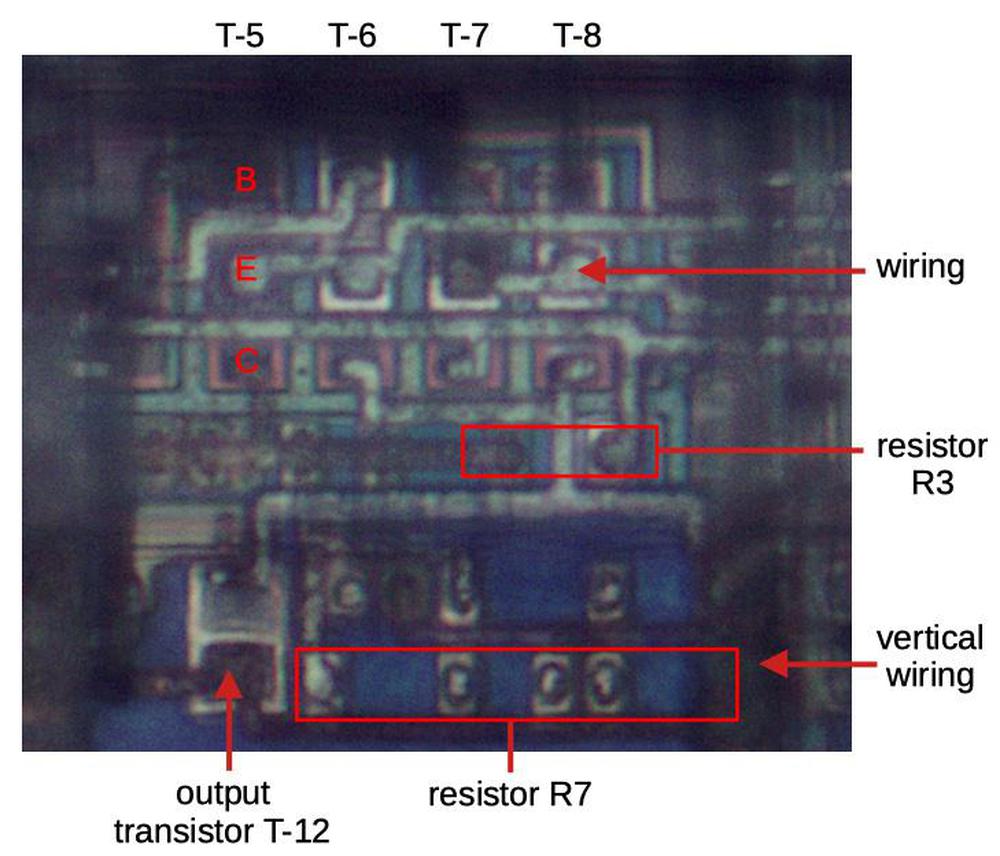
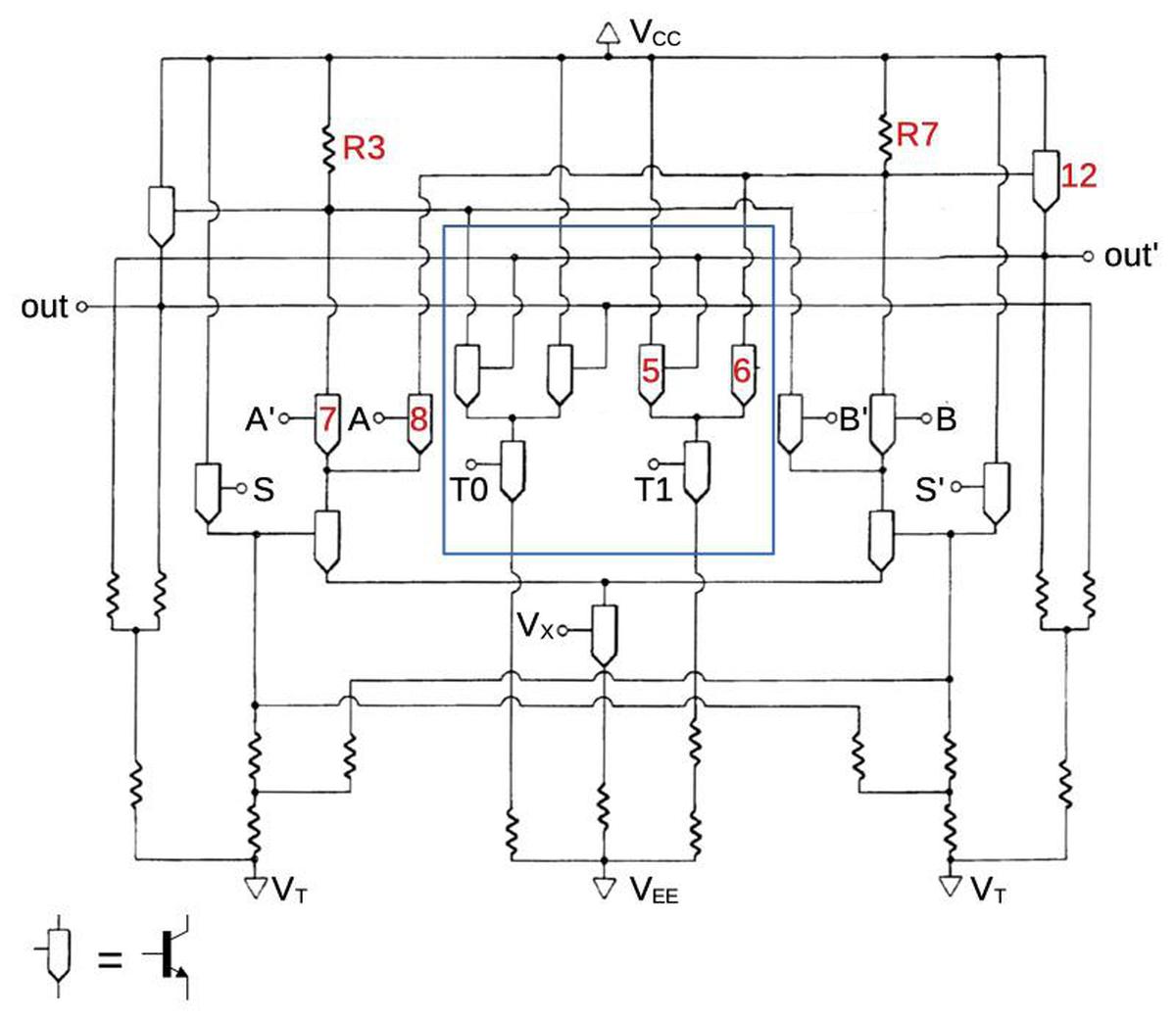
Below, I've indicated some of the components in the previously-highlighted half-cell. The wiring on the bottom metal layer customizes this cell for a particular function. Looking at this wiring, you can see that the emitters (E) of transistors T-5 and T-6 are connected, as are the emitters of transistors T-7 and T-8. The collectors (C) of transistors T-6 and T-8 are connected to the base of the output transistor T-12. The collector of transistor T-7 is connected to resistor R3. The wiring in the upper metal layers is shadowy and less clear. The vertical wiring along the sides provides power to the circuit. Other faint vertical wires are connected to the bases of transistors T-7 and T-8.
By studying the die closely, I traced out the circuitry for the gate and found it was a SELECT gate. The schematic below is from the patent; I modified it to match the gate I traced out. Note that IBM used its own symbol for a transistor as I've indicated at the bottom. I've marked the transistors and resistors from the photo above in red. The circuit has six transistors for testing, in the blue box.16 As you can see, one DCS gate takes a lot of components: 17 transistors and 18 resistors. This is one reason the density of the bipolar logic chips is so low.
This shows the circuitry of one logic gate. Larger functional blocks such as adders were constructed by combining multiple gates. The full computer contains hundreds of thousands of these gates, implementing the processor and its control circuitry.
Conclusion
This bipolar logic chip illustrates the advanced technology of the ES/9000 mainframe.17 IBM pushed the limits of technology in everything from integrated circuit construction to ceramic modules to cooling systems. After all this effort, however, sales of the ES/9000 were underwhelming and couldn't slow the advance of microcomputers. Two years after the announcement, IBM had installed about 3600 of them, largely the lower-end models.18 In comparison, about 20 million personal computers were being sold per year, about 10,000 times the volume. Mainframes were 21.6% of computer industry revenue and dropping, less than half of personal computer revenue (44.5% of the industry). In 1997, IBM's bipolar processors reached the end of the road as IBM fully moved to CMOS processors.
I announce my latest blog posts on Twitter, so follow me @kenshirriff. I also have an RSS feed.
If you're interested in the TCM, you should definitely watch Dave Jones' teardown video below, as well as the videos where he attempts to remove the chips with hot air and a heating plate before finally succeeding. Thanks to Dave for sending me the chips as well as letting me use his photos.
Notes and references
-
For more information, the IBM ES/9000 type 9121 was described in detail in a series of articles in the IBM Journal of Research and Development, May 1991. The most relevant articles: The IBM Enterprise System/9000 Type 9121 air-cooled processor describes how the processor was implemented, Differential current switch—High performance at low power describes the Differential Current Switch logic, IBM System/390 air-cooled alumina thermal conduction module describes the structure and manufacturing of the TCM in detail, IBM Enterprise System/9000 Type 9121 Model 320 air-cooled processor technology. The Sept 1992 issue has other relevant articles, including A four-level VLSI bipolar metallization design with chemical-mechanical planarization, Improved performance of IBM Enterprise System/9000 bipolar logic chips. Also see The Design of the ES/9000 module and High performance packaged electronics for the IBM ES9000 mainframe. IBM's announcement of the ES/9000 provides a good summary. ↩
-
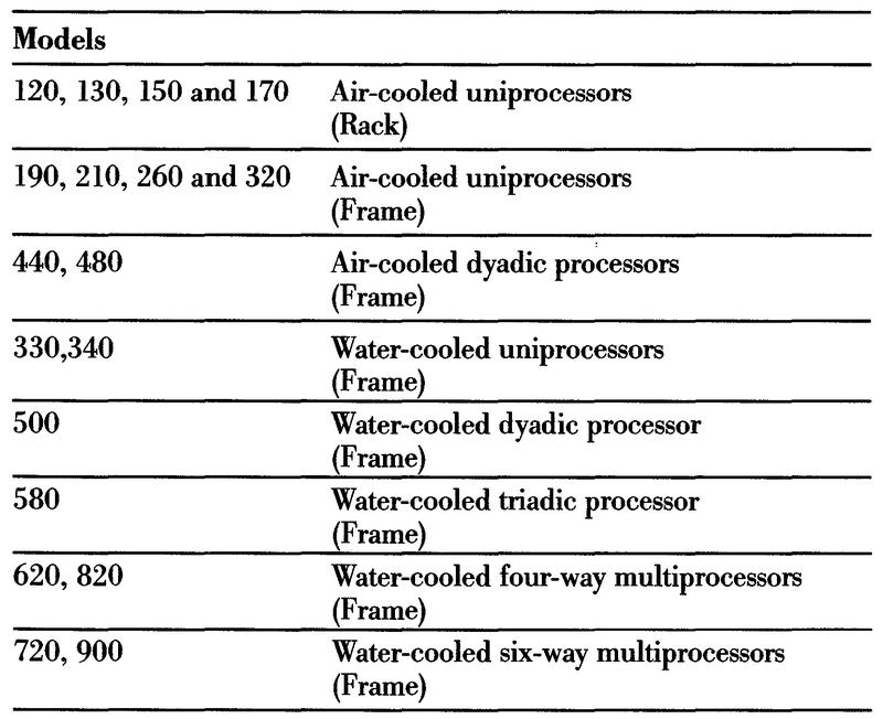
It's a bit tricky to keep track of IBM's naming and numbering schemes. The first distinction is between the architecture and the computers that implement the architecture. Enterprise Systems Architecture/390 (ESA/390) was IBM's mainframe architecture for the 1990s, continuing the path from System/360 and System/370. The ESA/390 architecture was implemented by several families of computers, including ES/9000, the CMOS-based 9672 Parallel Enterprise Server, the microprocessor-based Enhanced S/390 MicroProcessor Complex, S/390 Integrated Server, and S/390 Multiprise. The ES/9000 had three main processor types: the low-end CMOS 9221 in an air-cooled rack, the midrange 9121 in an air-cooled frame, and the large water-cooled 9021. (Confusingly, bigger numbers indicate a smaller system.) The 9121, the processor type in the middle, is the one I'm discussing in this blog post. Each processor type had several model numbers, as described below.
The different ES/9000 models, from the reference guide. The two-way and three-way multiprocessors are called "dyadic" and "triadic".The ES/9000 family covered an enormous range of performance levels; the largest model provided over 100 times the performance of the smallest. The sizes varied widely too. The rack-mounted 9221 was designed for an office and took about 6 square feet of floor space, while the 9121 in the middle was roughly refrigerator-sized, occupying 15 to 24 square feet. The water-cooled 9021 was the classic room-filling mainframe, sized at 88 to 180 square feet. Roughly speaking the low-end ES/9000 9221 was a replacement for the IBM 9370 office-environment "super-mini computer", the air-cooled ES/9000 9121 was a replacement for the IBM 4381, while the water-cooled ES/9000 9021 was a replacement for the larger IBM 3090 systems. ↩
-
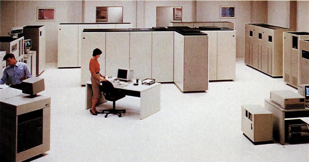
IBM was a leader in industrial design, from their computers to the architecture of their buildings and even their logo, as discussed in the book The Interface: IBM and the Transformation of Corporate Design. In the 1950s and 1960s, the design for IBM's computers concealed the internal circuitry, rather than showing it off like many other systems. Instead, IBM expressed the "inherent drama" of computing through spinning tape drives and other peripherals.
A large ES/9000 installation with the water-cooled 9021 processor. From IBM ESCON brochure.My opinion is that IBM's design style fell apart in the 1980s with the loss of dramatic consoles and tape drives, leaving just the featureless boxes. To make things worse, these boxes were stripped of subtle detailing such as their pedestal bases and accent trim, leaving units that wouldn't look out of place in a Soviet paper mill. The ES/9000 won a 1991 design award, however, so some people must like the design more than I do. ↩
-
The ES/9000 had five TCMs. The Central Processor Element (CPE) is the microcoded CPU, the module that executes the instructions. The Buffer Control Element (BCE) implements a 64- or 128-kilobyte high-speed cache with error correction, and also handles virtual memory. The System Control Element (SCE) manages the flow of data between the different parts of the computer. (The System Control Element is especially important in a two- or three-processor system.) The Channel Control Element (CCE) controls the I/O channels and is essentially a separate I/O processor. The system can also have an optional Vector Control Element (VCE) for vector arithmetic.
I was unable to conclusively determine the function of Dave's TCM. The large number (16) of memory chips suggests the cache in the Buffer Control Element (BCE), but this paper says the BCE has 26 memory chips. Possibly the chips are holding the microcode for the Central Processor Element (CPE). ↩
-
The ceramic module has two layers of complex thin-film wiring visible on top. This wiring has a surprising purpose: it allows modifications and bug fixes to be made to the module. By cutting wires with a laser and attaching new wires, signals can be re-routed.
Closeup of an IC location, showing the thin-film wiring on top. Courtesy of Dave Jones.IBM calls the modification of computer wiring an Engineering Change or EC. Back in the 1950s, an engineer could easily perform an engineering change by adding and removing wires from a mainframe's wire-wrapped backplane. The printed-circuit boards of the System/360 made changes more difficult, but IBM developed a special "delete" tool to drill out a trace on the circuit board, allowing modification.
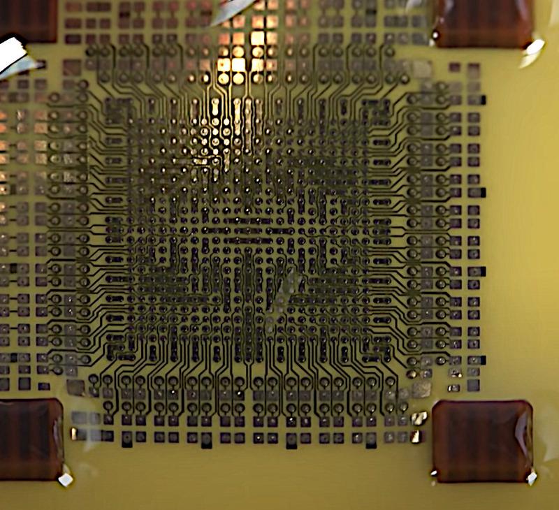
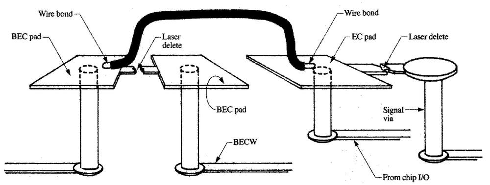
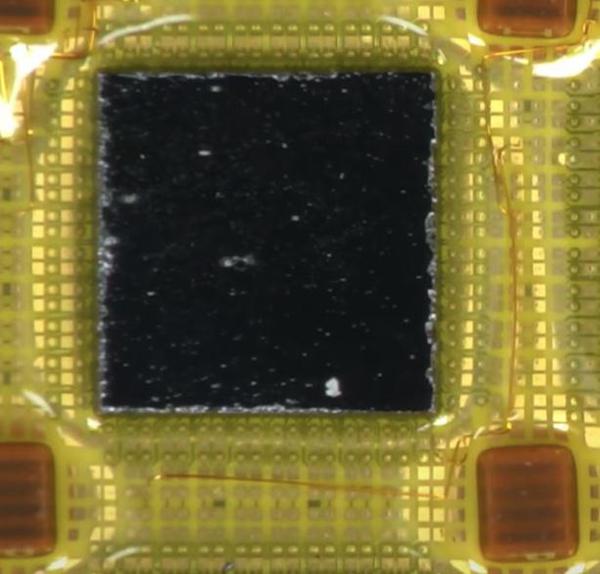
This diagram shows how an Engineering Change is made to an EC/9000 TCM. Parts of the thin-film wiring are cut with a laser, and a wire is attached to the special EC pads. From this paper.The introduction of the ceramic TCM raised the issue of how could engineering changes be made when the wiring was encased in ceramic. (Discarding the expensive module wasn't an attractive choice.) The solution was to put exposed wiring on the surface of the module, wiring that could be modified as necessary. This consisted of two layers of polyimide plastic (Kapton) with thin-film wiring. Instead of connecting the IC to the ceramic wiring directly, each chip signal went to an EC pad on the surface. The original trace could be vaporized with a laser, and a modification wire (gold-plated cadmium-copper alloy) ultrasonically bonded to the EC pad. The photo below shows a chip with some EC wires.
Closeup of the module showing Engineering Change wires next to the die. The smaller reddish-brown objects are capacitors. Courtesy of Dave Jones.In some cases it was necessary to remove a chip from the TCM. As Dave Jones found, unsoldering a chip is very difficult due to the thermal mass of the TCM. IBM invented a focused infrared machine to unsolder a chip. It combined a vacuum chip pick-up tool and infrared heater, along with a bias heater underneath the substrate to heat the whole TCM. A special prism ensured alignment of the new chip while a "mirror substrate" provided temperature feedback. This illustrates how the development of the ES/9000 required the invention of new, specialized tools. ↩
-
These bipolar chips were created using an IBM technology called ATX-4 that achieved almost five times the density of IBM's earlier ATX-1 chips. IBM described three advanced features of these transistors. First, they used a polysilicon base contact self-aligned with the emitter, reducing stray capacitance by a factor of 3. Second, the transistors were surrounded by deep trenches that allowed transistors to be closely packed. Third, they used a very thin implant for the base and optimized doping for the collector. These features improved the density and performance of the transistors. ↩
-
It's interesting to compare the complexity of the bipolar chip with a CMOS microprocessor at the same time. I did some rough estimates of transistor and gate counts, comparing the ES/9000 to a contemporary microprocessor. Each bipolar chip has 85,000 transistors. A CMOS processor from 1991, such as the MIPS R4000, has 1,350,000 transistors, almost 16 times as many, showing the huge density advantage of MOS over bipolar.
Looking at gates shows an even larger advantage for CMOS. The bipolar chip implements 2620 DCS gates, of which about half are used. For the CMOS processor, I'll estimate 6 transistors for a 3-input gate; subtracting the 16-kilobyte cache in the MIPS R4000 yields about 100,000 gates, a factor of 70 more than the bipolar chip.
Comparing a 121-chip TCM to a microprocessor yields a different story, with a TCM a bit more complex than a microprocessor. The TCM has roughly 144,000 gates and 256 kilobytes of cache, compared to 100,000 gates and 16 kilobytes of cache for the microprocessor. Thus, my estimate is that a TCM has 44% more gates than a contemporary microprocessor. Taking into account the R4000's external, off-chip cache, the cache sizes are comparable. The ES/9000 uses five TCMs for the processor, which works out to about 7 times the gates of the R4000.
Cross-section of a transistor in the IC. From Advancing the state of the art in high performance logic and array technology.The four metal layers of the chip are also highly advanced. The wiring in the chips is made from aluminum-copper alloy sandwiched with titanium to support high current density. The wiring layers are double-insulated with silicon dioxide and silicon nitride to prevent shorts from developing over time. Each layer of the chip is polished flat (planarized) with chemical-mechanical polishing. Even the vias between wiring layers are complex, created by a "damascene stud" method. The vias are constructed by creating holes with reactive ion etching, filling them with metal, and then polishing away excess metal. ↩
-
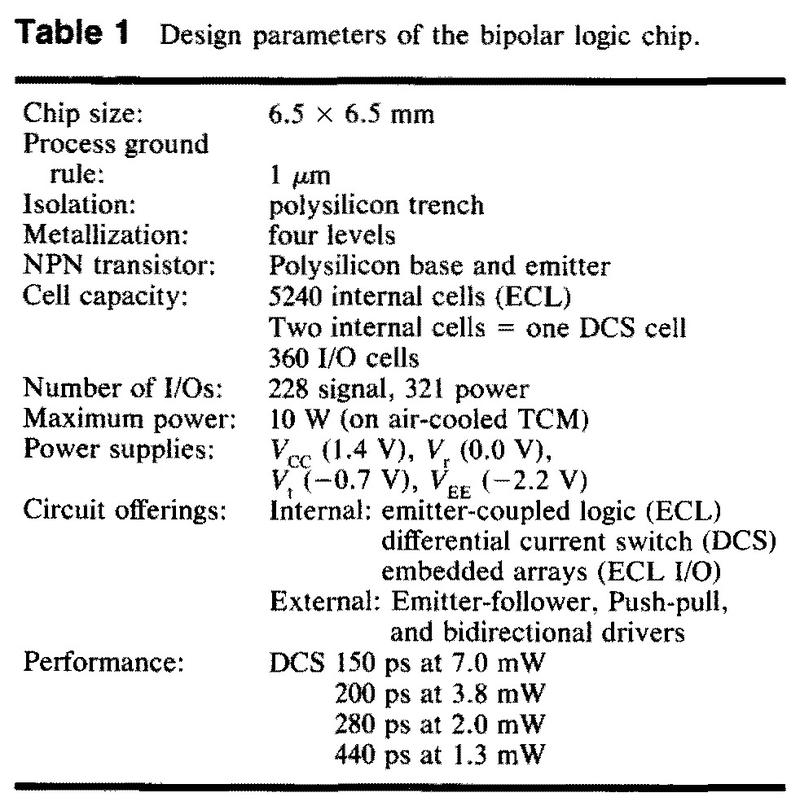
Here's a summary of the chip's parameters from IBM Enterprise System/9000 Type 9121 Model 320 air-cooled processor technology.
Design parameters of the chip. -
If you're familiar with ECL (Emitter-Coupled Logic), DCS is similar except it uses differential inputs instead of reference-controlled inputs. Although ECL and DCS both use a current-switching differential amplifier, ECL inputs are compared to a reference voltage, rather than the complemented input. (In IBM's ECL circuitry, the reference voltage is ground, so a negative signal is a logic 0 and a positive signal is a logic 1.)
The key performance benefit of ECL and DCS logic is that transistors are never completely turned on, i.e. saturated. A transistor is relatively slow to get out of saturation, so a logic family such as TTL that saturates transistors is slower. ↩
-
One fairly obscure logic family supported by the chip is NTL, Non-Threshold Logic. NTL is similar to ECL, but without the reference voltage and reference transistors. As a result, NTL gates don't switch on and off sharply, but change in a more analog fashion with the input voltage. One advantage of NTL is that it uses one half-cell instead of the two used by ECL, so you can fit more NTL gates on a chip. NTL also consumes less power than ECL. However, its performance was poorer and it was more sensitive to noise, so it was rarely used in the ES/9000. NTL is described in more detail in this patent. ↩
-
Each resistor has multiple taps (gray boxes) allowing 15 different resistance values to be obtained. Gates with various speed/power tradeoffs can be constructed by using different resistances: the DCS family supports high, medium, low, and ultra-low power gates. (Most of the circuitry is low and ultra-low power.) The 0.2 pf capacitors were used for ECL speedup and for delay elements. ↩
-
Why do these chips require so many solder balls? There's some theory behind it. In the 1960s, E. F. Rent at IBM noticed a relationship between the number of components in an integrated circuit and the number of pins it required. Specifically, as the number of components increased, the number of pins required also increased, according to a power law. This became known as Rent's rule. As IBM increased the complexity of the logic chips, the number of solder bumps increased correspondingly. Chips in the IBM 3080 computer (1980) had an 11×11 grid of solder balls, while the IBM 3090's chips (1985) had a 17×17 grid. (Numbers from this paper.) The chip I examined has a 27×27 grid, but since the chips were limited by the number of I/O connections and half the gate were unused, it seems that this was insufficient. ↩
-
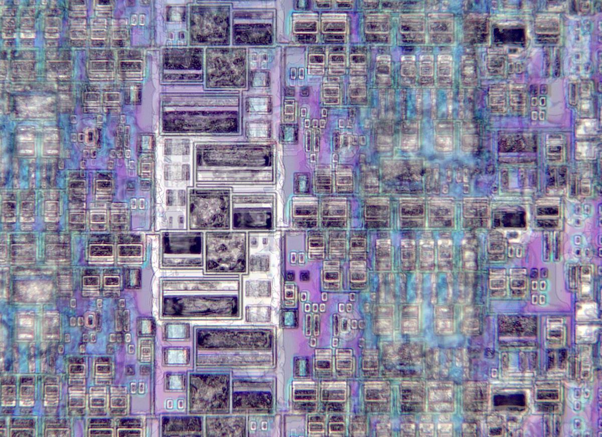
The image below shows some cells from the chip's I/O circuitry. These cells have a different structure from the cells for the logic gates. These cells include larger transistors to provide the necessary output current.
Die photo showing I/O cells. This die photo was formed from a stack of images. -
The SELECT operation (
SA+S'B) can implement multiple operations. For instance, setting B=0 implements S AND A. (For this gate, the redundant transistors can be omitted.) Setting A=B' implements S XOR A. (XOR is inconvenient to implement in most logic families but simple with DCS). Wiring the output back to A results in a latch: when S is high, the output value is held, but when S is low, the latch is loaded from B. An inverter is trivial with DCS: because of the differential signaling, a signal can be inverted simply by switching the two lines. ↩ -
Curiously, IBM's articles about the ES/9000 expand the DCS acronym as both Differential Current Switch and Differential Cascode Current Switch. The term cascode refers to "a two-stage amplifier that consists of a common-emitter stage feeding into a common-base stage." Essentially, it refers to how DCS has two layers of switching transistors, compared to the single layer in a typical ECL gate. ↩
-
Each DCS gate has about 6 additional transistors for test purposes. The problem is how to detect a faulty logic gate. In most logic families, a faulty gate will typically have the output stuck at 0 or 1. By running various test sequences through the circuit, this stuck bit can be detected. However, since a DCS gate uses differential logic, it can end up with a fault where both differential outputs are approximately the same, for instance, if the current sink fails. This is difficult to detect with tests since it is unpredictable how this signal will be interpreted by other gates. This non-determinism makes it hard to detect a faulty gate. The solution is to add test circuitry to each gate. The test circuitry will force an indeterminate output to a 0 or a 1, depending on which test circuit is activated. This makes the tests deterministic and a faulty gate can be detected. This seems like a weird corner case, but it was important enough for IBM to add a substantial amount of circuitry to each gate. The test circuit is described in more detail in this patent. ↩
-
In the 1980s, IBM faced the problem that it was the reigning computer company with its advanced mainframes, but it was encountering competition from microcomputers. Although microcomputers were technically inferior and much less powerful, they were much cheaper and rapidly increasing in power. The book The Innovator's Dilemma is the classic guide to this sort of problem. Incumbents often ignore the risk from disruptive technologies but IBM took the "right" approach and developed the IBM PC (1981) to take advantage of microprocessors. Although the IBM PC was extremely successful, IBM lost control of the PC architecture and personal computers devoured the mainframe market. It will be interesting to see what happens to Intel in the analogous situation as ARM processors gain functionality and cut into the market for technologically-advanced x86 chips. ↩
-
According to Computerworld, the adoption of ES/9000 was slow, with 3600 installed almost two years after introduction. Of the installations, 47% were low-end rack-mounted systems, 36% were air-cooled frame systems, and 17% were high-end water-cooled systems. IBM had over half the mainframe market, well ahead of Fujitsu, Hitachi, and NEC. ↩

12 comments:
Reading your article, it sounds like IBM could have used fewer chips with less exotic cooling if they'd used custom CMOS instead of the bipolar gate arrays.
What was the advantage of their approach? Was there one? The TCM looks steampunk compared to contemporary processor chips of the era.
J: IBM used CMOS chips in the low-end ES/9000 system, as you suggest. But the bipolar chips were faster, so IBM used them in the high-end systems despite the need for exotic cooling. By 1997, the performance of CMOS had improved to the point that IBM abandoned the bipolar chips.
I met some of the brilliant people that developed this incredible packaging technology. They essentially continued to brute force their way into computing as they did with their mainframes of the 1960s, using lots of (superlative) mechanical engineering and cost is no object engineering. Engineers’ paradise. They all have one of these substrates in their offices to this day! Incredibly enough, they kept going in that direction through the early 2000 with the Z-series, I still remember scratching my head when they proudly showcased one of the newer versions of these. Visiting Poughkeepsie a few years ago was heartbreaking though, as the site is half empty and falling apart in disrepair.
Visiting Poughkeepsie a few years ago was heartbreaking though, as the site is half empty and falling apart in disrepair.
Let's hope that's included in the US Repair program of your new administration.
Very cool piece of tech (well, as long as the oil doesn't leak). DCS logic isn't really uncommon -- we just call it "LVDS" today.
Surely it must have been obvious by 1991 that they were sinking a fortune into a losing strategy. If the IBM brain trust had worked on improving CMOS processes instead, I've gotta think we'd be that much farther ahead.
I note that during the time period that Engineer's Paradise, and cost is no object thinking was being felt in other parts of IBM. I remember my dad coming home from work at IBM from 1990 onward telling us how many of his co-workers were being offered "buyouts" to retire early. He got out just in time before the big 20,000 head count "blood-letting" in 1994. Just like Kodak in a lot of ways.
IBM was a far more innovative company than such as Microsoft and Apple. As far as I can see their focus was on avoiding anti-trust action in 80s, as was happening to Bell Telephones. This perhaps accounts for the kid-glove treatment of Microsoft in the early days.
But Microsoft had no such compunctions when dealing with Lotus Notes and Netscape.
Re : Carpet Bomberz Inc's comment . I saw the 1994 "blood-letting" as a broker. I recall the whoops that went up, with IBM shares shooting up in Wall Street from my corner in Singapore. Always thought that it was pretty ghoulish to celebrate that thousands of people being thrown out of jobs. But that is "creative destruction" for you.
IBM really pushed the technological envelope. AT&T/Bell System as well. They made everything themselves and it's interesting to see (1) the price/performance ratio, and (2) how their products departed from everyday industrial and consumer equipment.
I remember tearing apart a Western Electric PBX line card once. It was a metal-core, ceramic insulated PCB. This was in the 70s. Their stuff was designed to be put into service and left there forever. I have a 1968 date coded WE 565 telephone on my desk. It is (with the exception of the "rubber" feet, which are corroding the steel chassis) as good as the day it was made.
Tektronix used the same dual differential pair structure to perform a variety of logic and analog multiplexing and amplification functions starting in the 1970s. I will have to take a second look now that I know about NTL (non-threshold logic), although there is little available online about it. Unfortunately all of the commercial transistor arrays suitable for implementing these functions like the CA3102 are out of production.
I made a teardown video of a TCM back in 2018:-
https://www.youtube.com/watch?v=q7QOBAdPDf8
also, B=1 implements S OR A
Post a Comment