The Yamaha DX7 digital synthesizer (1983) was the classic synthesizer in 1980s pop music. It uses two custom digital chips to generate sounds with a technique called FM synthesis, producing complex, harmonically-rich sounds. Each note was implemented with one of 32 different patterns of modulation and summing, called algorithms. In this blog post, I look inside the sound chip and explain how the algorithms were implemented.
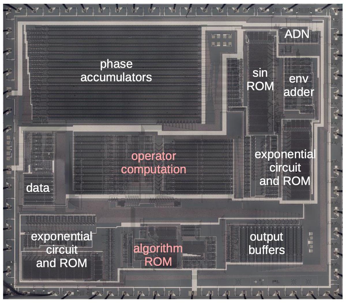
The die photo above shows the DX7's OPS sound synthesis chip under the microscope, showing its complex silicon circuitry. Unlike modern chips, this chip has just one layer of metal, visible as the whitish lines on top. Around the edges, you can see the 64 bond wires attached to pads; these connect the silicon die to the chip's 64 pins. In this blog post, I'm focusing on the highlighted functional blocks: the operator computation circuitry that combines the oscillators, and the algorithm ROM that defines the different algorithms. I'll outline the other functional blocks briefly. Each of the 96 oscillators has a phase accumulator used to generate the frequency. The sine and exponential functions are implemented with lookup tables in ROMs. Other functional blocks apply the envelope, hold configuration data, and buffer the output values.
The DX7 was the first commercially successful digital synthesizer, using a radically new way of generating sounds. Instead of the analog oscillators and filters of an analog synthesizer, the DX7 generates sounds digitally, using a technique called FM synthesis. The idea is that you start with a sine wave (the carrier signal) and perturb it with another signal (the modulating signal). The modulating signal changes the phase (and thus the frequency) of the carrier, creating complex harmonic structures. The custom chips inside the DX7 made this possible at an affordable price.
FM synthesis
I'll briefly explain how FM synthesis is implemented.1 The DX7 supports 16 simultaneous notes, with 6 operators (oscillators) for each note, 96 oscillators in total. However, to minimize the hardware requirements, the DX7 only has a single digital oscillator circuit. This circuit calculates each operator individually, in sequence. Thus, it takes 96 clock cycles to update all the sounds. To keep track of each oscillator, the DX7 stores 96 phase values, an index into the sine wave table. By incrementing the index at a particular rate, a sine wave is produced at the desired frequency.
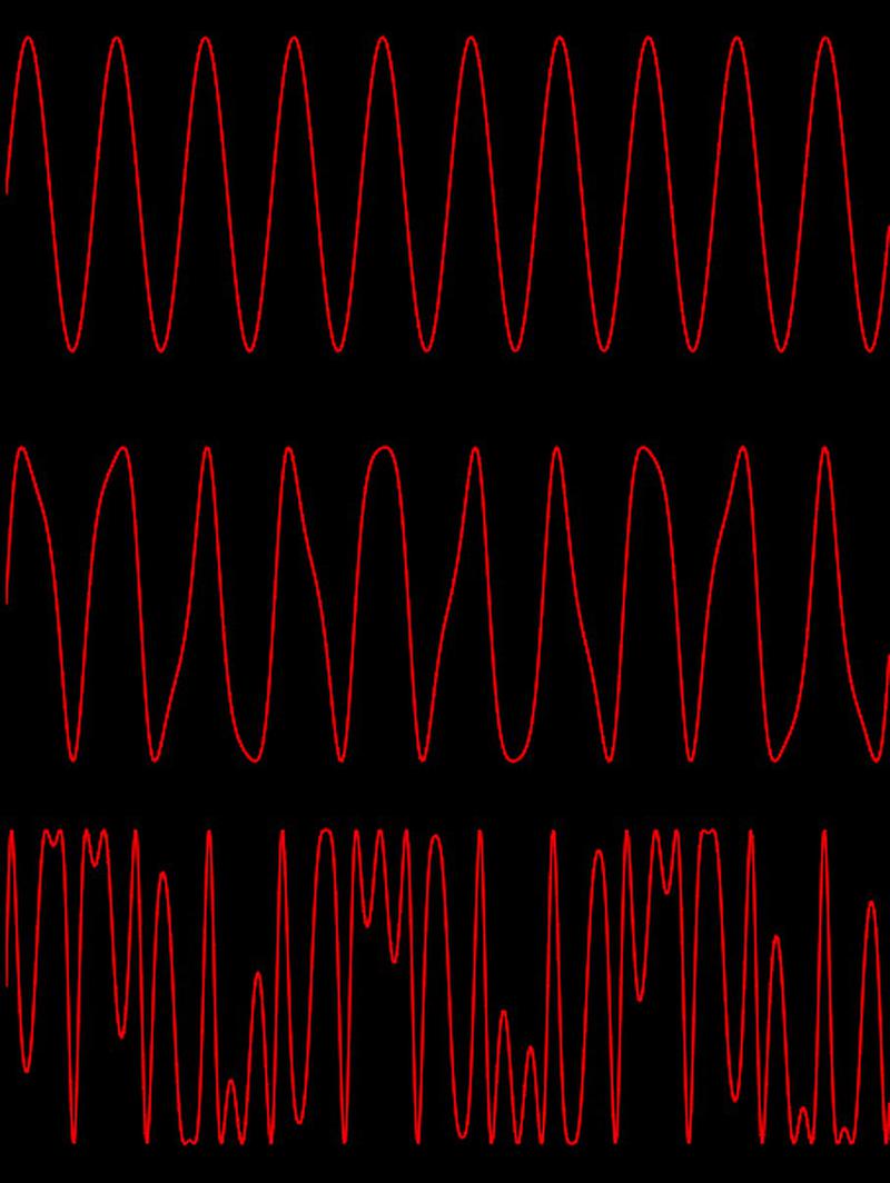
The idea of FM synthesis is to modulate the index into the sine wave table; by perturbing the index, the output sine wave is modified. The diagram below shows the effects of modulation. The top curve shows a sine wave, generated by stepping through the sine wave table at a fixed rate. The second curve shows the effects of a small amount of modulation, perturbing the index into the table. This distorts the sine wave, compressing and stretching it. The third curve shows the effects of a large amount of modulation. The index now sweeps back and forth across the entire table, distorting the sine wave unrecognizably. As you can see, modulation can produce very complex waveforms. These waveforms have a rich harmonic structure, yielding the characteristic sound of the DX7. (I made a webpage here where you can experiment with the effects of modulation.)
Algorithms
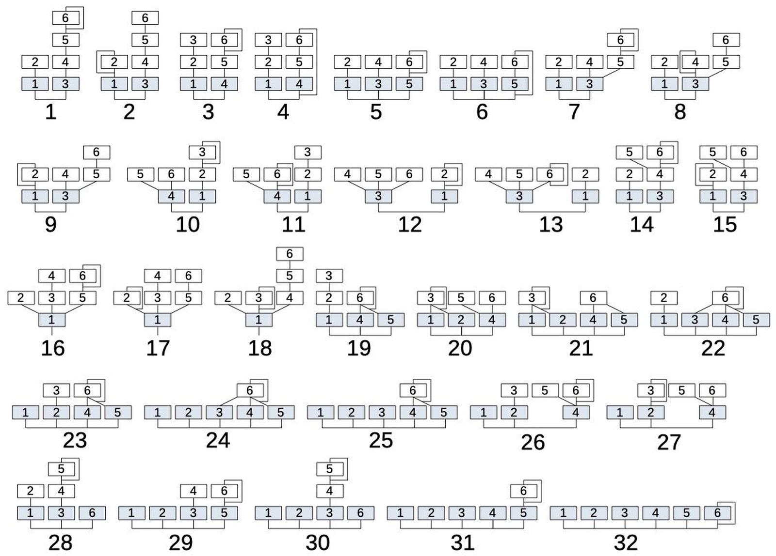
The above section illustrated how two oscillators can be combined with modulation. The DX7 extends this principle, generating a note by combining six oscillators through modulation and summing. It implements 32 different ways of combining these oscillators, illustrated below, and calls each one an algorithm. The different algorithms provide flexibility and variety in sound creation. Multiple levels of modulation create harmonically-rich sounds. On the other hand, multiple output operators allow different sounds to be combined. An electric piano sound, for example, could have one sound for the hammer thud, a second sound for the body of the tone, and a third sound for the ringing tine, all varying over time.
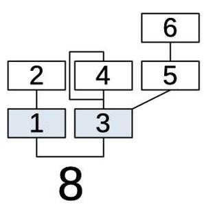
Looking at algorithm #8, for example, shows the structure of an algorithm. Each box represents an operator (oscillator). Operators 1 and 3 (in blue), are combined to form the output. The remaining operators provide modulation, as indicated by the lines. Operator 2 modulates operator 1. Operators 4 and 5 are combined to modulate operator 3, providing a complex modulation. Operator 6, in turn, modulates operator 5. Finally, the line looping around operator 4 indicates that operator 4 modulates itself. Since each modulation level can vary over time, the resulting sound can be very complex.
Shift-register storage
To understand the DX7's architecture, it's important to know that the chip uses shift registers, rather than RAM, for its storage. The idea is that bits are shifted from stage to stage each clock cycle. When a bit reaches the end of the shift register, it can be fed back into the register or a new bit can be inserted. For the phase accumulators, the shift registers are 96 bits long since there are 96 oscillators. Other circuits use 16 bit-shift registers to hold values for the 16 voices. The shift register circuitry (below) is dense, but even so, it takes up a large fraction of the chip.
The use of shift registers greatly affects the design of the DX7 chip. In particular, values cannot be accessed arbitrarily, as in RAM. Instead, values can only be used when they exit the shift register, which makes the circuit design much more constrained. Moreover, circuits must be carefully designed so that each path of a computation takes the same number of cycles (e.g. 16 cycles). Shorter paths must be delayed as necessary.2
I want to emphasize how unusual this chip is, compared to a microprocessor. You might expect that an algorithm is implemented with code, for example reading operator 2, applying modulation to operator 1, and then storing the result in operator 1. Instead, computation happens continuously in the chip, with data moving into the circuitry every clock cycle as it comes from the shift registers. The chip is more like an assembly line with bits constantly moving on many conveyor belts, and circuits steadily operating on bits as they move by. An advantage of this approach is that every clock cycle, calculations happen in parallel in multiple parts of the chip, providing much higher performance than a microprocessor could in the 1980s.
Implementation of the algorithms
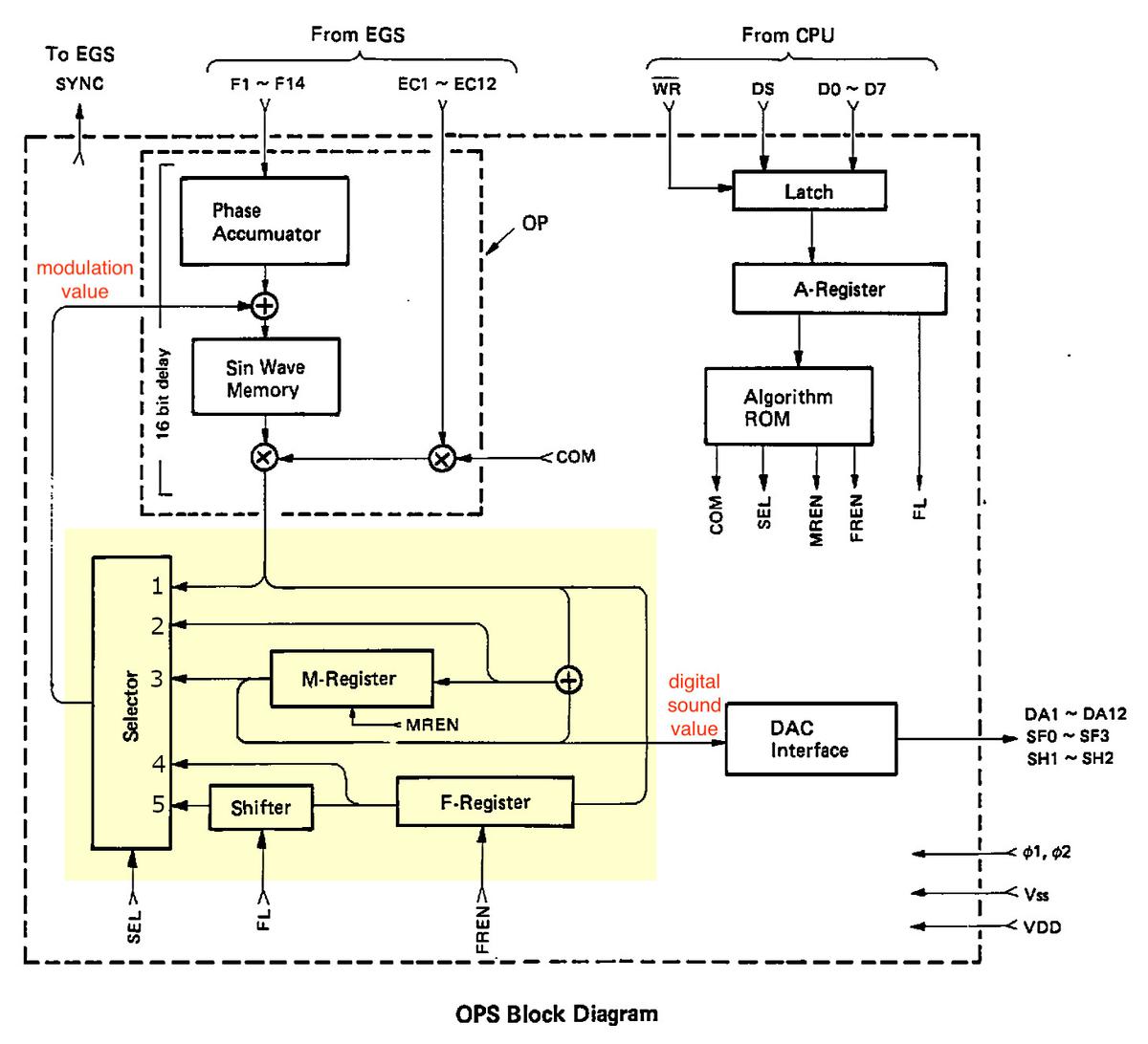
The block diagram below shows the overall structure of the OPS sound chip. The idea is that the envelope chip (EGS) constantly provides frequency (F) and envelope control (EC) values at the top. The DX7's control CPU updates the algorithm (A) if the user selects a new one. The sound chip generates digital data (DA) for the 16 voices, which is fed out at the right. (The DX7's digital-to-analog converter circuitry (DAC) converts these digital values to the analog sound from the synthesizer.)
In more detail, the circuitry in the upper left generates the phase values for the 96 oscillators and looks up the values in the sine wave table. In the lower-left, the highlighted block implements the algorithm, producing two outputs. This block contains its own storage: the memory (M) register and feedback (F) register. It generates a modulation value that modulates the index into the sine wave table. It also produces the digital sound value that is the output from the chip. (This highlighted block is the focus of this article.) At the right, the CPU specifies the algorithm number; the algorithm ROM specifies the algorithm by generating control signals COM, SEL, and so forth.
The DX7 has 96 oscillators, which are updated in sequence. The cycle of 96 updates takes place as shown below. In the first clock cycle, computation starts for operator 6 of voice (channel) 1. In the next clock cycles, operator 6 processing starts for voices 2 through 16. Next, operator 5 is processed for the 16 voices, and likewise for operators 4 to 1. At the end of this cycle, all the notes have been updated. Two factors are important here. First, operators are processed "backward", starting at 6 and ending at 1. Second, for a particular voice, there are 16 clock cycles between successive operators. This means that 16 cycles are available to compute each operator.
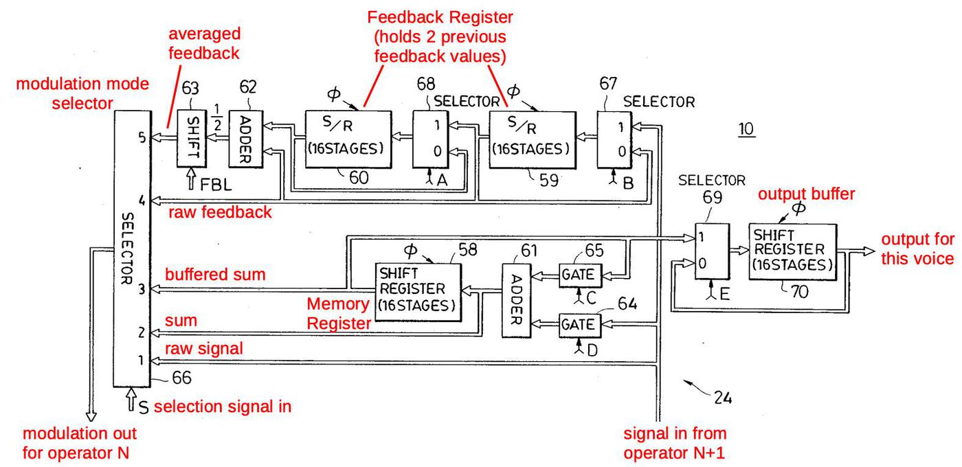
The diagram below provides more detail of highlighted block above, the circuitry that modulates the waveform according to a particular algorithm. The effect of modulation is to perturb the phase angle before lookup in the sine wave table.3 At the bottom right, the signal from operator N+1 enters, and is used to compute the modulation for operator N, exiting at the bottom left.
The key component is the selector at the left, which selects one of the five modulation choices, based on the control signal S or SEL. Starting at the bottom of the selector, SEL=1 selects the unmodified signal from the input operator; this implements the straightforward modulation of an operator by another. Next, SEL=2 uses the value from the adder (61) for modulation. This allows an operator to be modulated by the sum of operators, for instance in algorithm 7. SEL=3 uses the delayed value from the buffer; this is used solely for algorithm 21, where operator 6 modulates operator 4. SEL=4 and SEL=5 use the self-feedback operator for modulation. Because the feedback value is buffered in the circuitry, it is available at any time, unlike other operators. SEL=4 is used to obtain delayed feedback, for instance when operator 6 modulates operator 4 in algorithm 19. (In most cases, feedback is applied immediately, for instance when operator 6 modulates operator 5, and this uses SEL=1.) SEL=5 handles the self-feedback case; the previous two feedback values are averaged to provide stability.4 The SEL=0 case is not shown; it causes no modulation to be selected so the operator is unmodulated.
Several control signals (A, B, C, D, E) also control the circuit. (Confusingly, the patent diagram below uses the names A and B for the feedback register enable (FREN) line. The memory register enable (MREN) lines are called C and D.) Signals A and B have the same value: they select if the feedback buffer continues to hold the previous value or loads a new value. Signals C and D control the buffer/sum shift register. If C is 1 and D is 0, the register holds its previous value. If C is 0 and D is 1, the input signal is loaded into the register. If both C and D are 1, the input signal is added to the previous value. This register can be used to sum two modulation signals, as in algorithm 7. But it is also used to hold and sum the output signals. (As a consequence, an algorithm can't sum modulation signals and outputs at the same time.) Signal E loads the algorithm's final output value into the output buffer (70). Signal E and buffer 70 are implemented separately, so I won't discuss them further.
The algorithm ROM
The algorithms are defined by a ROM with 9-bit entries that hold the selector value (SEL), the control signals MREN and FREN (A,C,D), and the compensation scaling value COM (which I explain later). Each algorithm needs 6 entries in the ROM to select the action for the 6 operators. Thus, the ROM holds 96 9-bit values.
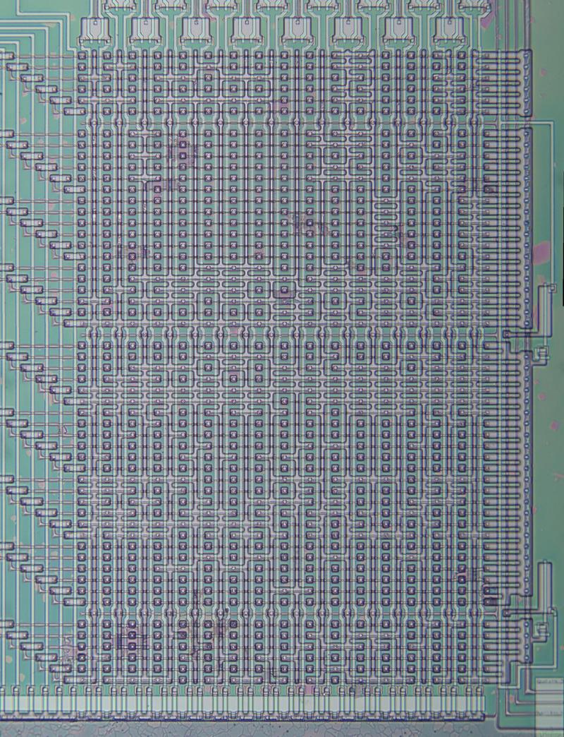
The photo below shows the algorithm ROM. It has 32 columns, one for each algorithm and 9 groups of 6 rows: one group for each output bit. From bottom to top, the outputs are three bits for the selector value SEL, two MREN lines and the FREN line, and three bits for the COM value. The groups of 6 diagonal transistors at the left of the ROM select the entry for the current operator.
The bits are visible in the pattern of the ROM. By examining the ROM closely, I extracted the ROM data. Each entry is formatted as "SEL / A,C,D / COM". (I only show three entries below; the full ROM is in the footnotes.5)
| Operator | ||||||
|---|---|---|---|---|---|---|
| Algorithm | 6 | 5 | 4 | 3 | 2 | 1 |
| 1 | 1/100/0 | 1/000/0 | 1/000/1 | 0/001/0 | 1/010/1 | 5/011/0 |
| 2 | 1/000/0 | 1/000/0 | 1/000/1 | 5/001/0 | 1/110/1 | 0/011/0 |
| ... | ||||||
| 8 | 1/000/0 | 5/001/0 | 2/111/1 | 0/001/0 | 1/010/1 | 0/011/0 |
To see how an algorithm is implemented, consider operator 8, for instance.6
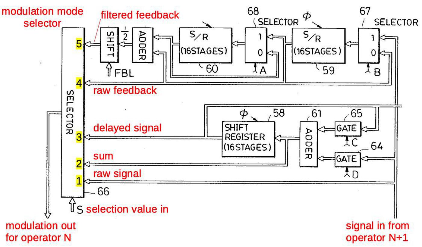
Processing of an algorithm starts with operator 6's signal value at the output of the operator block and operator 5's modulation is being computed. Table column 6 above shows SEL=1, A,C,D=000. In the modulation circuit (below), SEL=1 selects the raw signal in (i.e. operator 6's value) for modulation. Thus, operator 6 modulates operator 5, the desired behavior for algorithm 8.
Next, (16 cycles later), operator 5's signal is at the output and operator 4's modulation is being computed. Column 5 of the table shows SEL=5, A,C,D=001. SEL=5 selects the filtered feedback register for self-modulation of operator 4. D=1 causes operator 5's value to be loaded into the shift register, in preparation for modulating operator 3.
Next, operator 4's signal is at the output and operator 3's modulation is being computed. Column 4 shows SEL=2 and A,C,D=111. Bits A (and B) are 1 to load the feedback register with operator 4's value, updating the self-feedback for operator 4. Bits C and D cause operator 4 to be added to the previously-stored operator 5 value. SEL=2 selects this sum for operator 3's modulation, so operator 3 is modulated by both operators 4 and 5. COM=1 indicates this operator is one of 2 outputs, so operator 3's value will be divided by 2 as it is computed.
Next, operator 3's signal is at the output and operator 2's modulation is being computed. Looking at the ROM, SEL=0 results in no modulation of operator 2. D=1 loads operator 3's signal into the summing shift register, in preparation for the output.
Next, operator 2's signal is at the output and operator 1's modulation is being computed. SEL=1 causes operator 1 to be modulated by operator 2. C=1 so the summing shift register continues to hold the operator 3 value, to produce the output. As with operator 3, COM=1 so operator 1's value will be divided by 2 when it is computed.
Finally, operator 1's signal is at the output and operator 6's modulation is being computed. SEL=0 indicates no modulation of operator 6. Control signals C and D are 1 so operator 1 is added to the register (which holds operator 3's value), forming the final output.
This process repeats cyclically, interleaved with processing for the 15 other voices. This section illustrates how a complex algorithm is implemented through the modulator circuitry, directed by a few control signals from the ROM. The other algorithms are implemented in similar ways.7
The modulation circuitry
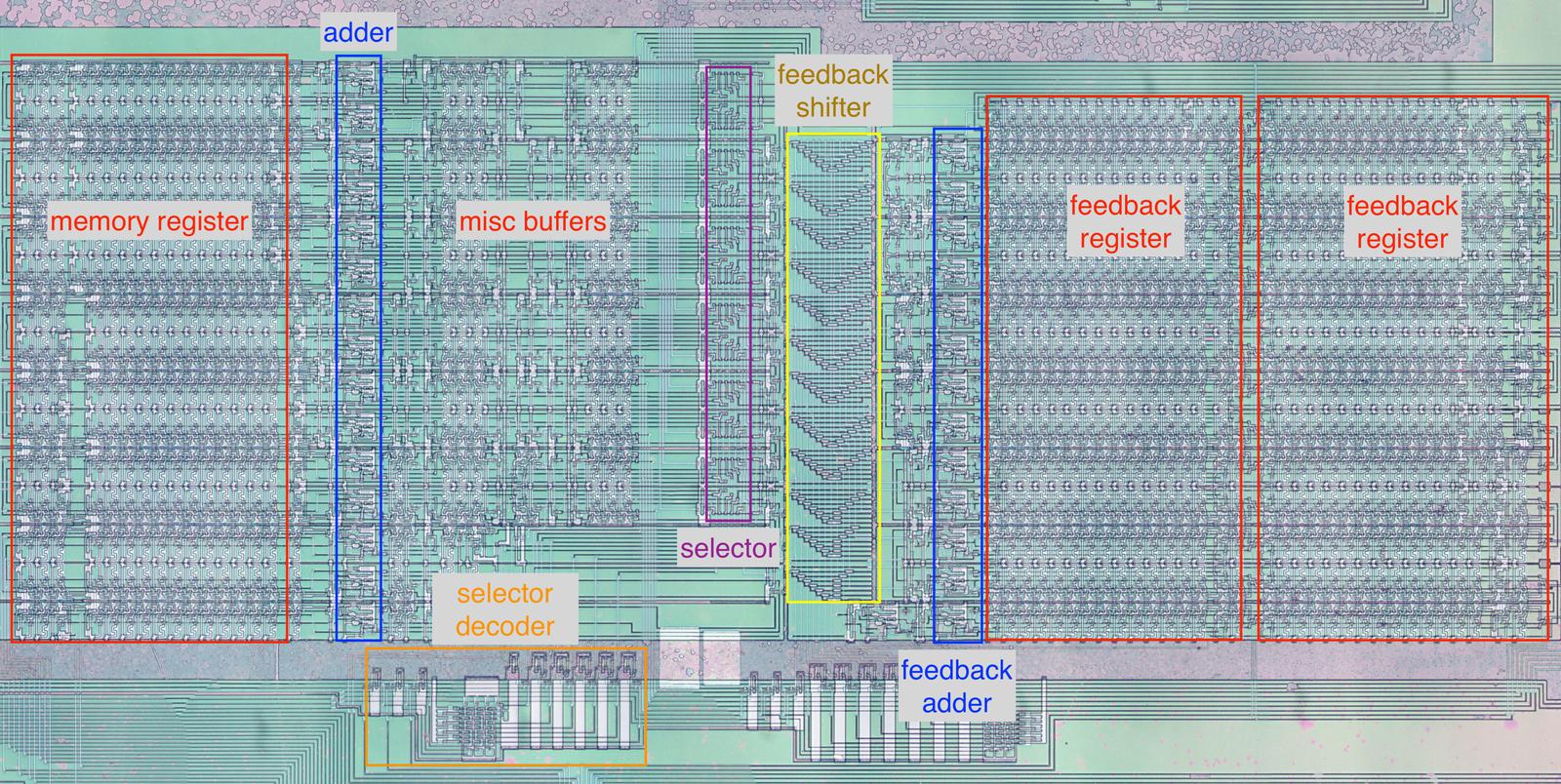
The diagram below shows the circuitry that computes the modulation and output; this functional block is in the center of the chip. The memory register (red) holds 16 values, one for each voice. To its right, the adder (blue) adds to the value in the memory register. The selector (purple), is the heart of the circuit, selecting which value is used for modulation. It is controlled by the selector decoder (orange) at the bottom, which activates a control line based on the 3-bit SEL value. At the far right, the two feedback registers (red) hold the last two feedback values for each of the 16 voices. The feedback adder sums two feedback values to obtain the average. The feedback shifter (yellow) scales the feedback value by a power of 2.
Shift registers
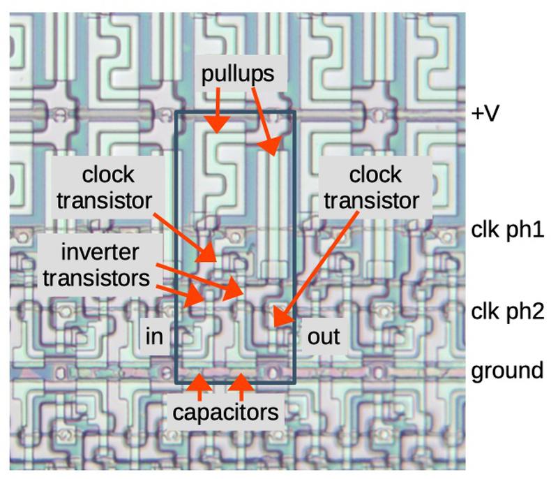
The schematic below shows how one stage of the shift register is implemented. The chip uses a two-phase clock. In the first phase, clock ϕ1 goes high, turning on the first transistor. The input signal goes through the inverter, through the transistor, and the voltage is stored in the capacitor. In the second phase, clock ϕ2 goes high, turning on the second transistor. The value stored in the capacitor goes through the second inverter, through the second transistor, and to the output, where it enters the next shift register stage. Thus, in one clock cycle (ϕ1 and then ϕ2), the input bit is transferred to the output. (The circuit is similar to dynamic RAM in the sense that bits are stored in capacitors. The clock needs to cycle before the charge on the capacitor drains away and data is lost. The inverters amplify and regenerate the bit at each stage.)
The diagram below shows part of the shift register circuitry as it appears on the die. The blue rectangle indicates one shift register stage. The power, ground, and clock wiring is in the metal layer, which was mostly removed in this image. Shift register stages are linked horizontally. Shift registers for separate bits are stacked vertically, with alternating rows mirrored.
The selector
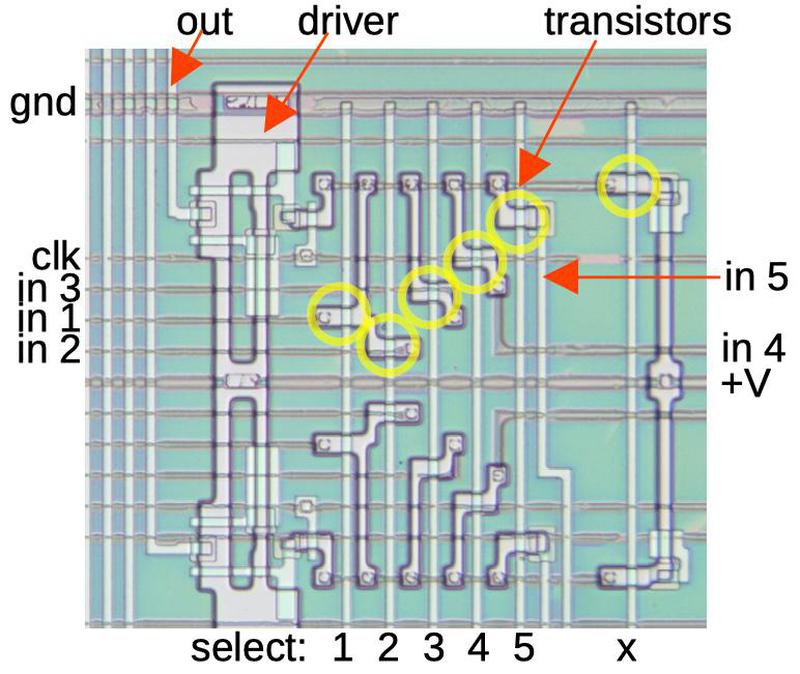
The selector circuit selects one of the five potential multiplexer values, based on the SEL input. The circuit uses five pass transistors (indicated in yellow) that pass one of the 5 inputs to the driver circuit and then the output. (A sixth transistor pulls the output high if none of the inputs is selected; I've labeled this "x".) The diagram below shows one selector in the top half, and a mirror-image selector below; there are 12 selector circuits in total. The circuit is built around the six vertical select lines. One select line is activated to select a particular value. This turns on the corresponding transistors, allowing that input to flow through the transistors. The result goes through another transistor to synchronize it to the clock, and then an inverter/buffer to drive the output line. The outputs go to the sine-wave circuit, where they modulate the input to the lookup table.
The adder
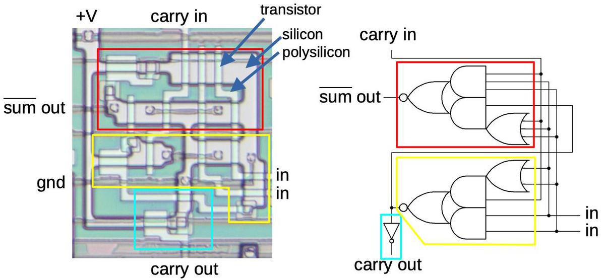
The chip contains multiple adders. Two adders are used in the modulation computation: one to sum operators and one to average the two previous feedback values. The adders are implemented with a standard binary circuit called a full adder. A full adder takes two input bits and a carry-in bit. It adds these bits to generate a sum bit and a carry-out bit. By combining full adders, larger binary numbers can be added.
The diagram above shows a full adder stage in the chip. The circuit is built from three relatively complex gates, but if you try the various input combinations, you can see that produces the sum and carry. (Due to the properties of NMOS circuits, it's more efficient to use a small number of complex gates rather than a larger number of simple gates such as NAND gates.)
One problem with binary addition is that it can be relatively slow for carries to propagate through all the stages. (This is the binary equivalent of 99999 + 1.) The solution used in the DX7 is pipelining: an addition operation is split across multiple clock cycles, rather than being completed in a single clock cycle. This reduces the number of carries in one clock cycle. Although a particular addition takes several clock cycles, the adders are kept busy with other additions, so one addition is completed every cycle.
The compensation (COM) computation
In the DX7, different algorithms have different numbers of oscillators in the output, which poses a problem An algorithm with 6 output oscillators (e.g. #32) would be six times as loud as an algorithm with 1 oscillator (e.g. #16), which would be annoying as the user changes the algorithm. To avoid this problem, the chip scales the level of output oscillators accordingly. For instance, the levels of output oscillators in algorithm #32 are scaled by 1/6 to even out the volumes. This factor is called COM (compensation) in the service manual and ADN (addition channel number) in the patent.8 To implement this scaling, the algorithm ROM holds the output count for each operator, minus 1. For example, algorithm #32 has six output oscillators, each one having a COM value of 5 (i.e. 6-1). For algorithm #1, the two output oscillators are 1 and 3: these have a COM value of 1 (i.e. 2-1). Operators that are used for modulation are not scaled, and have a COM value of 0.
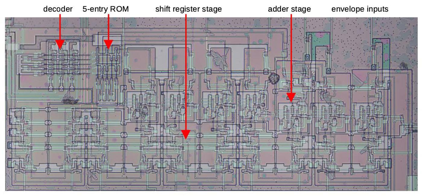
Recall that the envelope scaling is accomplished by adding base-2 logarithms. The COM scaling also uses logarithms, which are subtracted to scale down the output level. A small ROM generates 6-bit logarithms for the COM values 1 through 5, corresponding to scale factors 2 through 6. The diagram below shows the COM circuitry, which is in the upper-right corner of the chip. At the left, the decoder and tiny ROM determine the logarithmic scaling factor from the number of inputs. This is added to the logarithmic envelope level that the chip receives from the envelope chip. The result goes through a few shift register stages for timing reasons.
Conclusion
The DX7's algorithm implementation circuitry is at the heart of the chip's sound generation. This circuitry is cleverly designed to implement 32 different algorithms at high speed with the limited hardware of the 1980s. The circuitry runs fast enough to process 16 voices sequentially, each with 6 separate oscillators, while producing outputs fast enough to produce audio signals. By taking advantage of the pipelined architecture built around shift registers, the chip processes a different oscillator during each clock cycle, a remarkable throughput. Overall, I'm impressed with the design of this chip. Its cutting-edge design was the key to the DX7's ability to provide dramatic new sounds at a low price. As a result, the DX7 defined the canonical sound of the 1980s and changed the direction of pop music.
I plan to continue investigating the DX7's circuitry, so follow me on Twitter @kenshirriff for updates. I also have an RSS feed. Also see my previous posts on the DX7: DX7 reverse-engineering, the exponential ROM, The log-sine ROM.
Thanks to Jacques Mattheij and Anthony Richardson for providing the chip and discussion.9
Notes and references
-
Note that the underlying frequency of the oscillator stays the same during modulation, but the phase is changed. Technically the DX7 uses phase modulation (PM) rather than frequency modulation (FM). The two are closely related—phase modulation with a signal is the same as frequency modulation with the derivative of the signal—so the difference is usually ignored. ↩
-
Another complication is that the chip is pipelined. It doesn't simply go through 96 clock cycles, updating one operator each cycle. Instead, the computations for an operator are spread across multiple clock cycles. The result is still that one operator calculation is completed per clock, but different parts of the circuitry are working on different operators at any particular time.
The reason for pipelining is to handle calculations that won't fit into one clock cycle. For instance, the chip adds 22-bit numbers. Propagating a carry through all 22 adder stages would take too long for one clock cycle. Instead, addition takes place in chunks of about 4 bits. The lowest 4 bits are added in one clock cycle, the next bits in the next clock cycle, and so forth. Thus, the propagation delay during one clock cycle is substantially reduced. The circuit still completes one addition per cycle, even though any particular addition takes multiple cycles. ↩
-
The diagram below from the patent shows how this is implemented. The modulation is added to the phase angle to create the index into the sine table, yielding the modulated signal. This signal is scaled by the envelope; instead of multiplying, the base-2 logarithms of both values are added. (Ignore ADN for now; I'll discuss it later.) Finally, the logs are converted back to linear values by an exponential ROM and circuit. The result is the modulated and scaled output signal. The steps in this box take exactly 16 clock cycles, which will turn out to be important. As a result, operator N's values enter the box at the same time that operator N+1's values exit the box. (Remember that operators are processed in reverse order: 6 down to 1.)
Diagram showing the construction of an operator, from the patent.I'll summarize the patent's mathematical notation in case anyone reads it. The phase angle, varying with time is ωt. kωt indicates the possible use of a frequency modifier k. The modulation function is f(ωmt), a function of the modulation frequency. The envelope, as a function of t, is A(t) for the amplitude or I(t) for the modulation index; that is, applied to an output operator or a modulating operator respectively. On the diagrams, Φ indicates the clock. ↩
-
When an operator provides feedback to itself (usually operator 6), the modulation uses a special path that averages the previous two values. The patent calls this an "anti-hunting" feature. I think this avoids wild oscillations from self-feedback. Suppose you have a situation where a large modulation signal produces a small output and a small modulation signal produces a large output. This would result in the signal oscillating between small and large every clock cycle, which would be unpleasant. Averaging the previous two values is essentially a low-pass filter and would prevent these wild oscillations. Also note that the self-feedback path allows the feedback level to be controlled by the FBL signal. This shifts the feedback signal, dividing it by a power of 2. ↩
-
The full algorithm ROM contents are below. The format is "SEL/ FREN MREN / COM value". Note that algorithm numbers are 1 to 32, while the ROM's binary addresses are 0 to 31.
↩Operator Algorithm 6 5 4 3 2 1 1 1/100/0 1/000/0 1/000/1 0/001/0 1/010/1 5/011/0 2 1/000/0 1/000/0 1/000/1 5/001/0 1/110/1 0/011/0 3 1/100/0 1/000/1 0/001/0 1/010/0 1/010/1 5/011/0 4 1/000/0 1/000/1 0/101/0 1/010/0 1/010/1 5/011/0 5 1/100/2 0/001/0 1/010/2 0/011/0 1/010/2 5/011/0 6 1/000/2 0/101/0 1/010/2 0/011/0 1/010/2 5/011/0 7 1/100/0 0/001/0 2/011/1 0/001/0 1/010/1 5/011/0 8 1/000/0 5/001/0 2/111/1 0/001/0 1/010/1 0/011/0 9 1/000/0 0/001/0 2/011/1 5/001/0 1/110/1 0/011/0 10 0/001/0 2/011/1 5/001/0 1/110/0 1/010/1 0/011/0 11 0/101/0 2/011/1 0/001/0 1/010/0 1/010/1 5/011/0 12 0/001/0 0/011/0 2/011/1 5/001/0 1/110/1 0/011/0 13 0/101/0 0/011/0 2/011/1 0/001/0 1/010/1 5/011/0 14 0/101/0 2/011/0 1/000/1 0/001/0 1/010/1 5/011/0 15 0/001/0 2/011/0 1/000/1 5/001/0 1/110/1 0/011/0 16 1/100/0 0/001/0 1/010/0 0/011/0 2/011/0 5/001/0 17 1/000/0 0/001/0 1/010/0 5/011/0 2/111/0 0/001/0 18 1/000/0 1/000/0 5/001/0 0/111/0 2/011/0 0/001/0 19 1/100/2 4/001/2 0/011/0 1/010/0 1/010/2 5/011/0 20 0/001/0 2/011/2 5/001/0 1/110/2 4/011/2 0/011/0 21 1/001/3 3/001/3 5/011/0 1/110/3 4/011/3 0/011/0 22 1/100/3 4/001/3 4/011/3 0/011/0 1/010/3 5/011/0 23 1/100/3 4/001/3 0/011/0 1/010/3 0/011/3 5/011/0 24 1/100/4 4/001/4 4/011/4 0/011/4 0/011/4 5/011/0 25 1/100/4 4/001/4 0/011/4 0/011/4 0/011/4 5/011/0 26 0/101/0 2/011/2 0/001/0 1/010/2 0/011/2 5/011/0 27 0/001/0 2/011/2 5/001/0 1/110/2 0/011/2 0/011/0 28 5/001/0 1/110/0 1/010/2 0/011/0 1/010/2 0/011/2 29 1/100/3 0/001/0 1/010/3 0/011/3 0/011/3 5/011/0 30 5/001/0 1/110/0 1/010/3 0/011/3 0/011/3 0/011/3 31 1/100/4 0/001/4 0/011/4 0/011/4 0/011/4 5/011/0 32 0/101/5 0/011/5 0/011/5 0/011/5 0/011/5 5/011/5 -
The DX7/9 service manual explains the steps of algorithms 1 and 21 in detail. ↩
-
Note that the algorithms are carefully designed with operator 6 on top and 1 on the bottom, so operators are modulated only by operators with a higher number. This is due to the implementation of the modulation circuitry which processes operators starting with 6 and ending with 1. The 32 algorithms make it look like almost anything is possible, but the hardware imposes several constraints that limit the possibilities. For instance, there is only one sum/delay register so you can't sum modulators and the output at the same time. You can't delay a non-feedback operator after an output takes place; for instance, algorithm 11 has 6 delayed to modulate 3, but only because there haven't been any outputs at that point. An algorithm can only have one self-feedback loop. ↩
-
The logarithmic COM values are:
COM binary value value 0 00.000 log2(1) 1 01.000 log2(2) 2 01.101 ≈log2(3) 3 10.000 log2(4) 4 10.011 ≈log2(5) 5 10.101 ≈log2(6) Since the computation is done with logarithms, the circuit subtracts these values (or equivalently adds the complement). This is equivalent to dividing by the number of outputs or multiplying by the reciprocal. Note that the COM input is one less than the number of outputs. Entry 0 is not explicitly stored in the ROM but results by default. If the result of the subtraction is negative, gates clamp the envelope at 0. ↩
-
For more information on the DX7 internals, see DX7 Technical Analysis, DX7 Hardware, OPLx decapsulated, and the video Emulating the DX7 the hard way. ↩






12 comments:
s/tine/tone/
Brian: an electric piano has a hammer hitting a wire tine, which generates the sound.
Thinking about this, how did they do the design before they built the masks and shipped this off to the fab? Did they have FPGAs back then or would they have made the mother of all breadboards and run it at a slower speed?
I would expect that doing a sound chip meant that you really wanted it to be running at the design speed so you could hear the results, as opposed to just looking at them on a 'scope.
It's just amazing that a team could design all this and come up with solutions and get it fabbed, especially when the computers of the time were so limited, so didn't provide the support tools that chip designers used now.
They must have gone through multiple spins of the chip to make this work!
John S: I'm quite sure that they couldn't use FPGAs to prototype it, FPGAs seem to have been born around 1983 (same as the DX7) and I think that the first ones were very expensive too (and limited).
But they did make the GS-1 three years earlier, which I think was their first official FM synth, it used 50 chips rather than the two used by the DX7! It seems that it had only one algorithm, but I guess that it could be seen as a breadboard version of a lot of the concepts used in the DX7 at least :)
There was also the CE20 which used the YM20100 and YM20110. I think those chips were different than the ones used in the two GS models.
I remember the DX7 marketing papers from the time. they showed a phone booth sized rack of cards that was a DX7 in all discrete logic. I’m sure they played with that for while before committing to the chip design
John S: According to Wikipedia, Verilog and VHDL were both developed in the early 1980s. So was the MAGIC VLSI design software. It seems likely that companies like Yamaha may have had proprietary software tools before then to aid in this sort of design.
That's great history, to learn how they made the DX7 chips using racks of cards with discrete logic. Must have been hell to debug and tweak and get running fast enough so they could hear what they were doing.
Thanks for all the hard work explaining it, totally fascinating!
Ken, great series. But this post had me a bit puzzled. The algorithms shown in this post are different from the algorithm drawing from the patent (as shown in the first post). They match the drawing in the service manual.
However, the text from footnote 7 is copied from one of the footnotes in the first post, and is now inaccurate: it mentions that in algorithm #11, operator 6 modulates operator 3. This was true with the patent's numbering scheme for algorithms, but with the numbering used in this post it should be corrected to algorithm #12.
Ken, thanks for these articles! I've been thinking about how to make an FM voice module for a modular synth I'm building, and your analysis has helped me figure out how I might do it - but using a microcontroller like RP2040, not shift registers and custom logic! I've played a DX7 so the idea of building something loosely based on it appeals to me.
I think the OPS and EGS were coded and simulated in Verilog or VHDL (lets say they used VHDL). After extensive testbenches (more code that simulates what external circuitry is doing, like the CPU for example) were coded, each and every circuit was checked using a CAE tool that displayed the resulting simulation waveforms. Each simulation for just a few milliseconds of "run time" must have taken hours back in the early 1980's and computers did not have very high speed or high resolution graphics like they have today. This is called functional simulation.
After the the VHDL code was "blessed" functionally, they laid out the circuits all in NAND gates (which can be built up into any digital circuit, counters, RAM, ROM, what have you). This was also done in VHDL. This allows them to see how the circuit timing will work across the whole chip design. This is called timing/route simulation.
After the timing/routing simulation was approved, that data was sent to an ASIC house. An ASIC is the forerunner of FPGAs. It is just a grid of millions of NAND gate on a substrate with no connections to any of them. The ASIC house then takes the routing information and lays down trace (route) layers to connect the NAND gates and using the timing data to be sure clock edges arrive to all the gates in time. The ASIC is now a prototype of what they coded the OPS and EGS chips to do within the timing constraints they desired.
It takes weeks to get just 1 wafer of ASICs (say 10) per design. So almost a year of simulations is done before an ASIC is sent out for fab. If anything was wrong in the design, you pretty much scrapped the ASIC (you only get one shot per fab), and more simulations are done to fix it, and that new data goes out for another "spin" of the ASIC. It was slow and tedious, but it was all we had and we liked it.
FPGAs have gates and flip flops (among other logic elements) in a grid with fixed wiring runs between them. In an FPGA, you send all the info to the chip to tell it how to make to wiring connections. And because those connections are RAM based, you can makes changes on the spot and try it again on the same FPGA until you get it right.
Once Yamaha had a working design, they could have taken the trace artwork from the ASIC house and have many places whip out ASICs for production. But once they had a good working ASIC, they redid it on their own silicon to get more performance. Hence the custom EGS and OPS chips.
I'm finishing up my research into the Yamaha VLSI "Digital Direct Synthesis - FM Modulation" chips utilized inside the Kenwood TS-850S HF Radio Transceiver. Kenwood outsourced Yahama to make these YM6631 and YM66312 revision in 1991. These chips, four to be exact, were placed onto a seperate CAR (Carrier circut board) inside the trancsiver, which created arbitary waveforms from a single, fixed-frequency clock creating specific RF frequencies to LO mixers including generating side tones when transmitting a carrier. Your article and research gives me great insight on how Yamaha accomplished this. Keep up the great work.
Post a Comment