If you've played around with electronic circuits, you probably know the 555 timer integrated circuit,1 said to be the world's best-selling integrated circuit with billions sold. Designed by analog IC wizard Hans Camenzind2, the 555 has been called one of the greatest chips of all time.
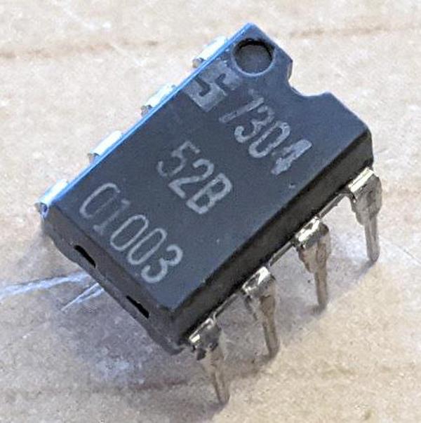
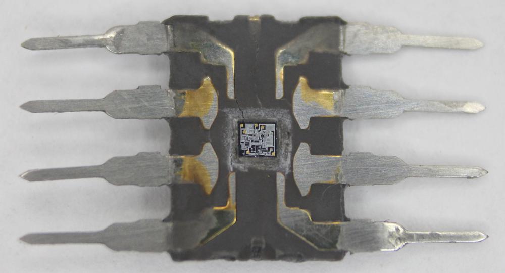
Eric Schlaepfer (@TubeTimeUS) recently came across the chip above, with a mysterious part number. He tediously sanded through the epoxy package to reveal the die (below) and determined that the chip is a 555 timer. Signetics released the 555 timer in mid-1972 4 and the chip below has a January 1973 date code (7304), so it must be one of the first 555 timers. Curiously, it is not labeled 555, so perhaps it is a prototype or internal version.3 I took detailed die photos, which I discuss in this blog post.
A brief explanation of the 555 timer
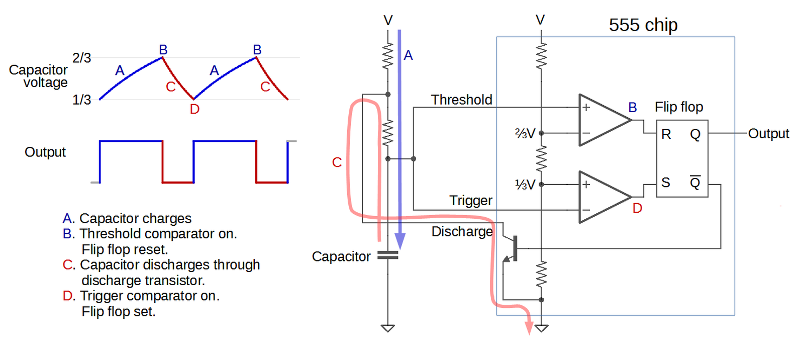
The 555 timer has hundreds of applications, operating as anything from a timer or latch to a voltage-controlled oscillator or modulator. The diagram below illustrates how the 555 timer operates as a simple oscillator. Inside the 555 chip, three resistors form a divider generating references voltages of 1/3 and 2/3 of the supply voltage. The external capacitor will charge and discharge between these limits, producing an oscillation. In more detail, the capacitor will slowly charge (A) through the external resistors until its voltage hits the 2/3 reference. At that point (B), the upper (threshold) comparator switches the flip flop off and the output off. This turns on the discharge transistor, slowly discharging the capacitor (C). When the voltage on the capacitor hits the 1/3 reference (D), the lower (trigger) comparator turns on, setting the flip flop and the output, and the cycle repeats. The values of the resistors and capacitor control the timing, from microseconds to hours.5
To summarize, the key components of the 555 timer are the comparators to detect the upper and lower voltage limits, the three-resistor divider to set these limits, and the flip flop to keep track of whether the circuit is charging or discharging. The 555 timer has two other pins (reset and control voltage) that I haven't covered above; they can be used for more complex circuits.
The structure of the integrated circuit
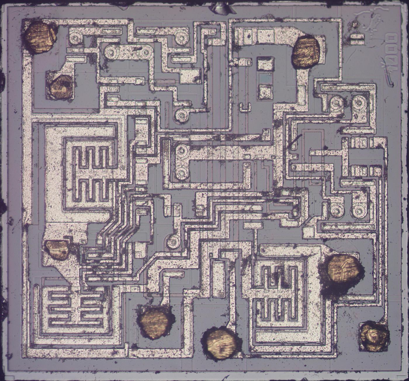
I created the photo below from a composite of microscope images. On top of the silicon, a thin layer of metal connects different parts of the chip. This metal is clearly visible in the photo as light-colored traces. Under the metal, a thin, glassy silicon dioxide layer provides insulation between the metal and the silicon, except where contact holes in the silicon dioxide allow the metal to connect to the silicon. At the edge of the chip, thin wires connect the metal pads to the chip's external pins.
The different types of silicon on the chip are harder to see. Regions of the chip are treated (doped) with impurities to change the electrical properties of the silicon. N-type silicon has an excess of electrons (negative), while P-type silicon lacks electrons (positive). In the photo, these regions show up as a slightly different color surrounded by a thin black border. These regions are the building blocks of the chip, forming transistors and resistors.
NPN transistors inside the IC
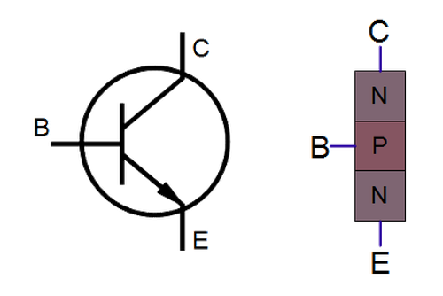
Transistors are the key components in a chip. The 555 timer uses NPN and PNP bipolar transistors. If you've studied electronics, you've probably seen a diagram of an NPN transistor like the one below, showing the collector (C), base (B), and emitter (E) of the transistor, The transistor is illustrated as a sandwich of P silicon in between two symmetric layers of N silicon; the N-P-N layers make an NPN transistor. It turns out that transistors on a chip look nothing like this, and the base often isn't even in the middle!
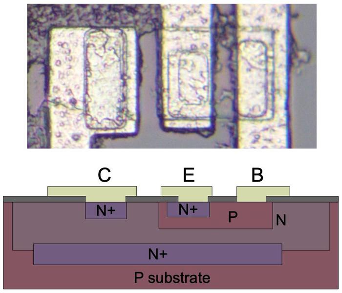
The photo below shows a closeup of one of the transistors in the 555 as it appears on the chip. The slightly different tints in the silicon indicate regions that have been doped to form N and P regions. The whitish areas are the metal layer of the chip on top of the silicon - these form the wires connecting to the collector, emitter, and base.
Underneath the photo is a cross-section drawing illustrating how the transistor is constructed. There's a lot more than just the N-P-N sandwich you see in books, but if you look carefully at the vertical cross-section below the 'E', you can find the N-P-N that forms the transistor. The emitter (E) wire is connected to N+ silicon. Below that is a P layer connected to the base contact (B). And below that is an N+ layer connected (indirectly) to the collector (C).6 The transistor is surrounded by a P+ ring that isolates it from neighboring components.
PNP transistors inside the IC
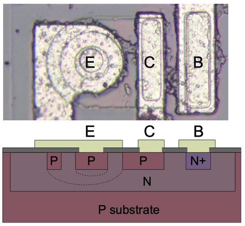
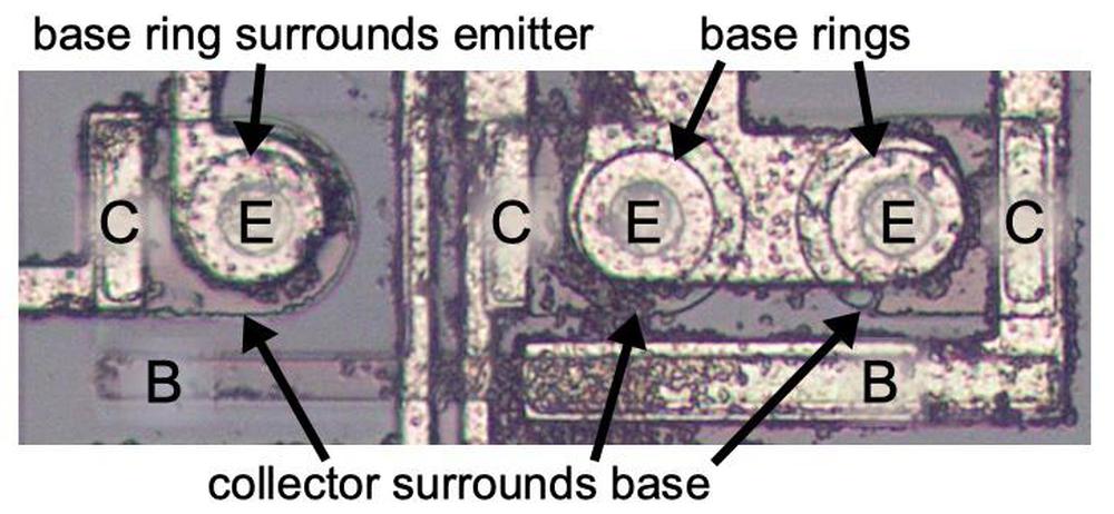
You might expect PNP transistors to be similar to NPN transistors, just swapping the roles of N and P silicon. But for a variety of reasons, PNP transistors have an entirely different construction. They consist of a small circular emitter (P), surrounded by a ring-shaped base (N), which is surrounded by the collector (P). This forms a P-N-P sandwich horizontally (laterally), unlike the vertical structure of the NPN transistors.
The diagram below shows one of the PNP transistors in the 555, along with a cross-section showing the silicon structure. Note that although the metal contact for the base is on the edge of the transistor, it is electrically connected through the N and N+ regions to its active ring in between the collector and emitter.
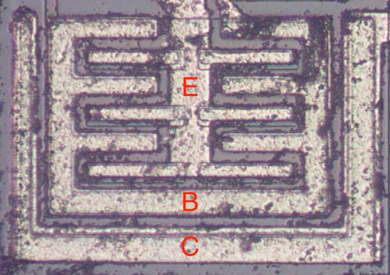
The output transistors in the 555 are much larger than the other transistors and have a different structure in order to produce the high-current output. The photo below shows one of the output transistors. Note the multiple interlocking "fingers" of the emitter and base, surrounded by the large collector.
How resistors are implemented in silicon
Resistors are a key component of analog chips. Unfortunately, resistors in ICs are large and inaccurate; the resistances can vary by 50% from chip to chip. Thus, analog ICs are designed so only the ratio of resistors matters, not the absolute values, since the ratios remain nearly constant.
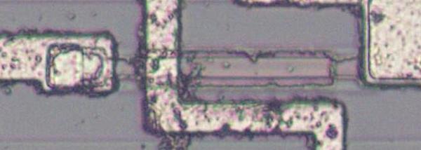
The photo above shows a 10KΩ resistor in the 555, formed from a strip of P silicon (pinkish gray), contacting metal wiring at either end. Other metal wires cross the resistor. The resistor has a spiral shape to fit its length in the available space. The resistor below is a 100KΩ pinch resistor. A layer of N silicon on top of the pinch resistor makes the conductive region much thinner (i.e. pinches it), forming a much higher but less accurate resistance.
IC component: The current mirror
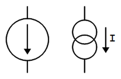
There are some subcircuits that are very common in analog ICs, but may seem mysterious at first. The current mirror is one of these. If you've looked at analog IC block diagrams, you may have seen the symbols below, indicating a current source, and wondered what a current source is and why you'd use one. The idea is you start with one known current and then you can "clone" multiple copies of the current with a simple transistor circuit, the current mirror.
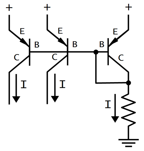
The following circuit shows how a current mirror is implemented with two identical transistors.7 A reference current passes through the transistor on the right. (In this case, the current is set by the resistor.) Since both transistors have the same emitter voltage and base voltage, they source the same current, so the current on the right matches the reference current on the left.8
A common use of a current mirror is to replace resistors. As explained earlier, resistors inside ICs are both inconveniently large and inaccurate. It saves space to use a current mirror instead of a resistor whenever possible. Also, the currents produced by a current mirror are nearly identical, unlike the currents produced by two resistors.
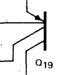
The three transistors above form a current mirror with two outputs. Note the three transistors share the base connection, tied to the collector on the right, and the emitters on the right are tied together. On the schematic, the two transistors on the right are drawn as a single two-collector transistor, Q19.
IC component: The differential pair
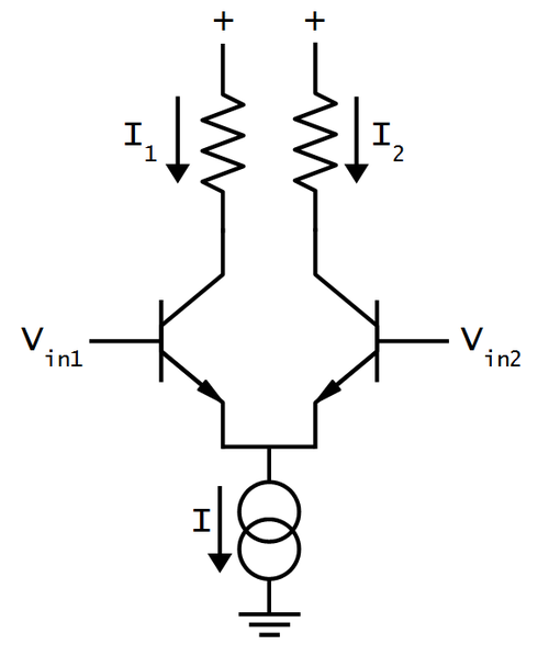
The second important circuit to understand is the differential pair, the most common two-transistor subcircuit used in analog ICs. 9 You may have wondered how a comparator compares two voltages, or an op amp subtracts two voltages. This is the job of the differential pair.
The schematic above shows a simple differential pair. The current source at the bottom provides a fixed current I, which is split between the two input transistors. If the input voltages are equal, the current will be split equally into the two branches (I1 and I2). If one of the input voltages is a bit higher than the other, the corresponding transistor will conduct exponentially more current, so one branch gets more current and the other branch gets less. A small input difference is enough to direct most of the current into the "winning" branch, flipping the comparator on or off. The 555 chip uses one differential pair for the threshold comparator and another for the trigger comparator.10
The 555 schematic interactive explorer
The 555 die photo and schematic11 below are interactive. Click on a component in the die or schematic, and a brief explanation of the component will be displayed. (For a thorough discussion of how the 555 timer works, see 555 Principles of Operation.)
For a quick overview, the large output transistors and discharge transistor are the most obvious features on the die. The threshold comparator consists of Q1 through Q8. The trigger comparator consists of Q10 through Q13, along with current mirror Q9. Q16 and Q17 form the flip flop. The three 5KΩ resistors forming the voltage divider are in the middle of the chip.12 Urban legend says that the 555 is named after these three 5K resistors, but according to its designer 555 is just an arbitrary number in the 500 chip series.
Conclusion
I hope you've found this look inside the 555 timer chip interesting. Next time you're building a 555 project, you'll know exactly what's inside the chip. I've written about the 555 timer before; this post is pretty much the same as that one but with a different die. I've also written about a CMOS version. Thanks to Eric Schlaepfer13 for providing the die; see his Twitter thread for background on this chip.
I announce my latest blog posts on Twitter, so follow me @kenshirriff and you won't miss an article! I also have an RSS feed.
Notes and references
-
The 555 timer is iconic enough to appear on mugs, bags, caps and t-shirts. Whole books are devoted to 555 timer circuits. ↩
-
The book Designing Analog Chips written by the 555's inventor Hans Camenzind is really interesting, and I recommend it if you want to know how analog chips work. Chapter 11 has an extensive discussion of the 555's history and operation. Page 11-3 claims the 555 has been the best-selling IC every year, although I don't know if that is still true. The free PDF is here or get the book. ↩
-
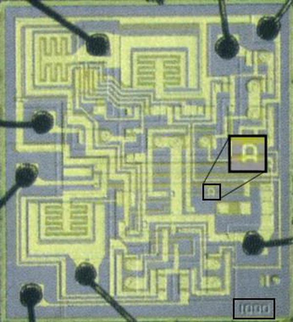
The die has the part number 1000 and revision "C", so this probably corresponds to the 01003 number on the package. I suspect this chip is the third mask revision of the original 555.
The first 555 die with the part number "1000" highlighted and the revision "A" magnified.The die of the first 555 timer version (above) is marked with the number "1000" and revision "A". I compared this image with the die photo that I took and I couldn't see any differences except the revision changed to "C". The mask changes must have been fairly subtle. (This image is at Wikipedia and IEEE Spectrum. The image is captioned as the die shot of the first 555 timer IC manufactured in 1971.) ↩
-
The 555 chip was introduced in mid-1972 according to Signetics Analog Applications page 149. ↩
-
The brilliant part of the 555 timer is that the oscillation frequency depends only on the external resistors and capacitor and is insensitive to the supply voltage. If the supply voltage drops, the 1/3 and 2/3 references drop too, so you might expect the oscillations to be faster. But the lower voltage charges the capacitor more slowly, canceling this out and keeping the frequency constant.
This voltage insensitivity is so tricky that the chip's designer didn't figure it out until near the end of the 555's design, but it made a big difference. The original design was more complex and required nine pins, which is a terrible size for an IC since there are no packages between 8 and 14 pins. The final, simpler 555 design worked with 8 pins, making the chip's packaging much cheaper. (See page 11-3 of Designing Analog Chips for the full story.) ↩
-
You might have wondered why there is a distinction between the collector and emitter of a transistor, when the typical diagram of a transistor is symmetrical. As you can see from the die photo, the collector and emitter are very different in a real transistor. In addition to the very large size difference, the silicon doping is different. The result is a transistor will have poor gain if the collector and emitter are swapped. ↩
-
For more information about current mirrors, check wikipedia, any analog IC book, or chapter 3 of Designing Analog Chips. ↩
-
The schematic has the unusual symbol below, which indicates a transistor with two collectors. The base is drawn on the same side as the emitter and collectors, which adds to the confusion. On the die, this transistor is implemented with two separate transistors, with the emitters and the bases wired together. Other circuits sometimes use a single transistor that has two physical collectors present.
This symbol indicates a transistor with two collectors. -
Differential pairs are also called long-tailed pairs. According to Analysis and Design of Analog Integrated Circuits the differential pair is "perhaps the most widely used two-transistor subcircuits in monolithic analog circuits." (p214) For more information about differential pairs, see wikipedia, any analog IC book, or chapter 4 of Designing Analog Chips. ↩
-
In the 555, the threshold comparator uses NPN transistors, while the trigger comparator uses PNP transistors. This allows the threshold comparator to work near the supply voltage and the trigger comparator to work near ground. The 555's comparators also use two transistors on each input (Darlington pair) to buffer the inputs. ↩
-
The 555 schematic used in this article is from the Philips datasheet. It is identical to the Signetics schematic p150. ↩
-
Note that the three resistors for the voltage divider are parallel and next to each other. This helps ensure they have the same resistance even if there are electrical variations across the silicon. ↩
-
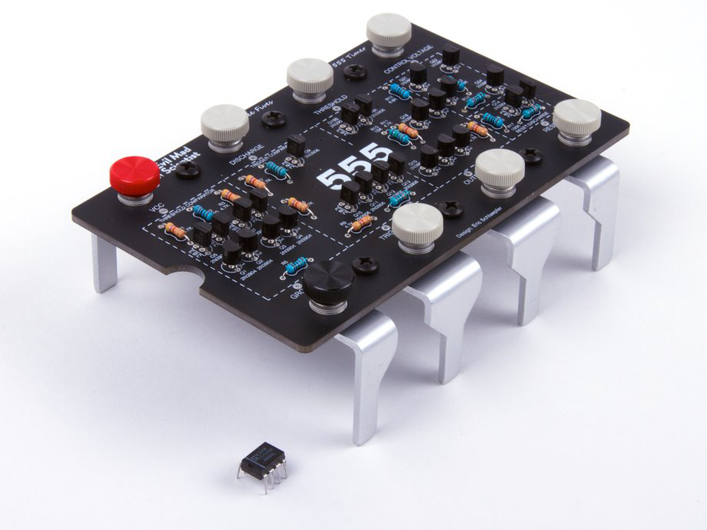
Evil Mad Scientist sells a very cool discrete 555 timer kit, duplicating the 555 circuit on a larger scale with individual transistors and resistors — it actually works as a 555 replacement. Their 555 footstool is also worth a look.
Large-size 555 timer created by Evil Mad Scientist Lab.

7 comments:
The interactive schematic / die explorer is an awesome addition to these blog posts.
Ken,
Fascinating article, a fan of your work on CuriousMarc's channel as well as here.
In health,
-est2
Waan soo dhawaynayaa kanaalka
Pretty cool article. Being in electronics of course we learned quite a bit about the 555 early on but I don't think anything ever got as detailed as this. I'm actually hooked to find out what else you have written.
I would have thought 741 was the most common analoge İÇ.
Sorry qaalada hore ee aan bixuyay qoraalka ayaa qalad waxaan aad usoo dhawaynayaa bogan casharadanna bogaadunayaa waayo wax badan ayaanka faa''day shikhsiyan
Can you explain why a 555 can explode like popcorn when you apply 9V between the output and GND?
Post a Comment