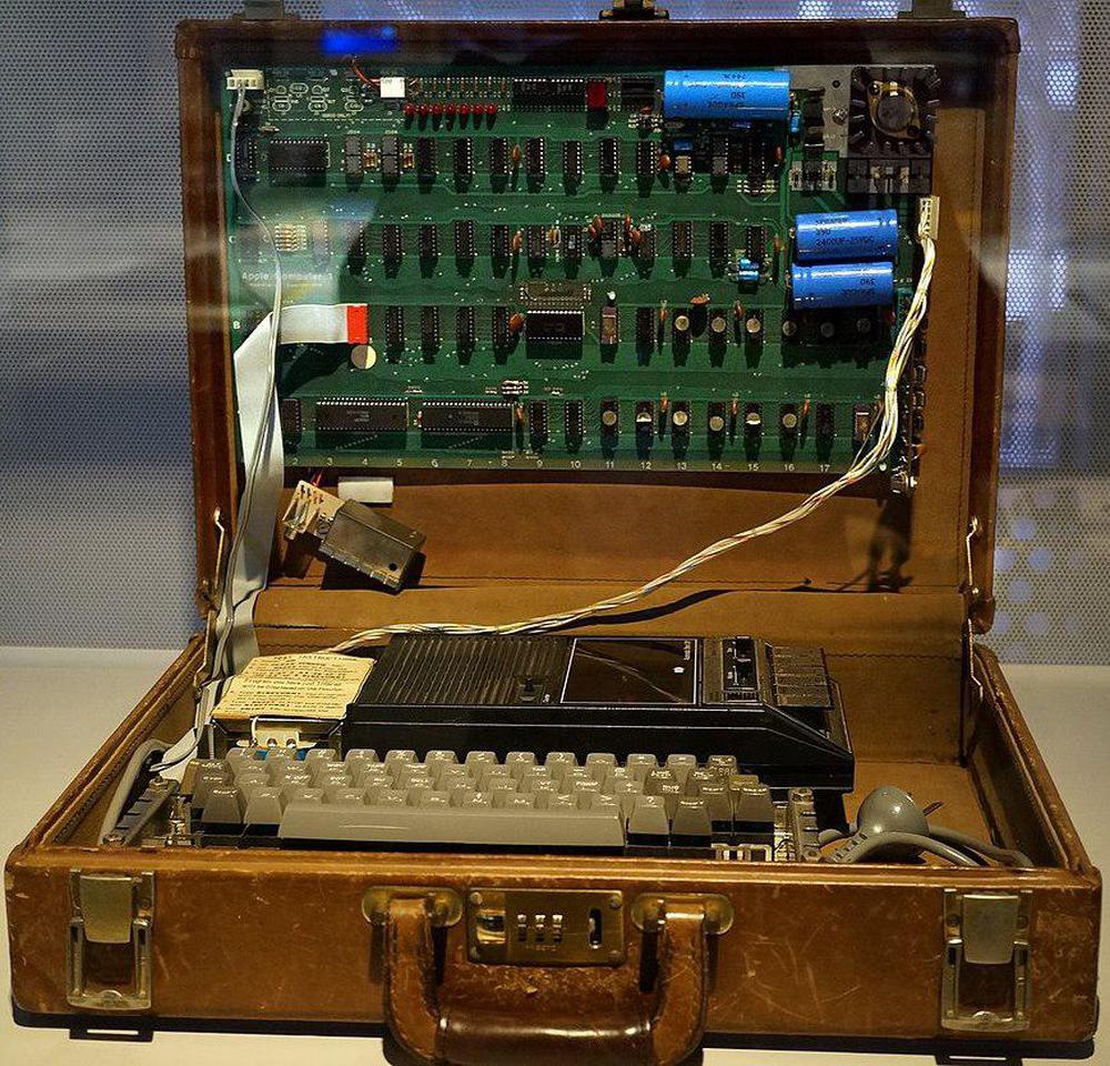
Apple's first product was the Apple-1 computer, introduced in 1976. This early microcomputer used an unusual type of storage for its display: shift register memory. Instead of storing data in RAM (random-access memory), it was stored in a 1024-position shift register. You put a bit into the shift register and 1024 clock cycles later, the bit pops out the other end. Since a shift-register memory didn't require addressing circuitry, it could be manufactured more cheaply than a random-access memory chip.1 The downside, of course, is that you had to use bits as they became available, rather than access arbitrary memory locations. The behavior of shift-register memory was a good match for video circuitry, though, since characters are displayed on the screen in a fixed, repeating order (left to right and top to bottom).2
Shift-register memory chips required clock pulses with high current and unusual voltages: from +5 volts to -11 volts. These pulses were provided by a special chip, the DS0025 Two-Phase MOS Clock Driver. This chip, introduced in 1969, was the first monolithic (i.e. integrated circuit) clock driver. In this blog post, I look inside the chip and explain how it was implemented.
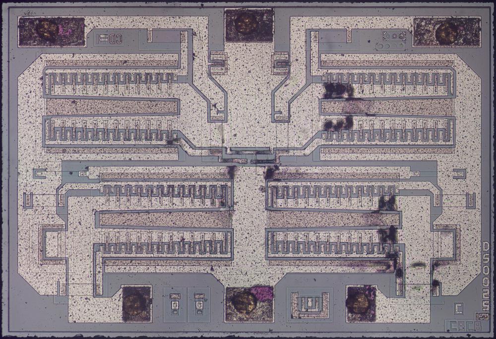
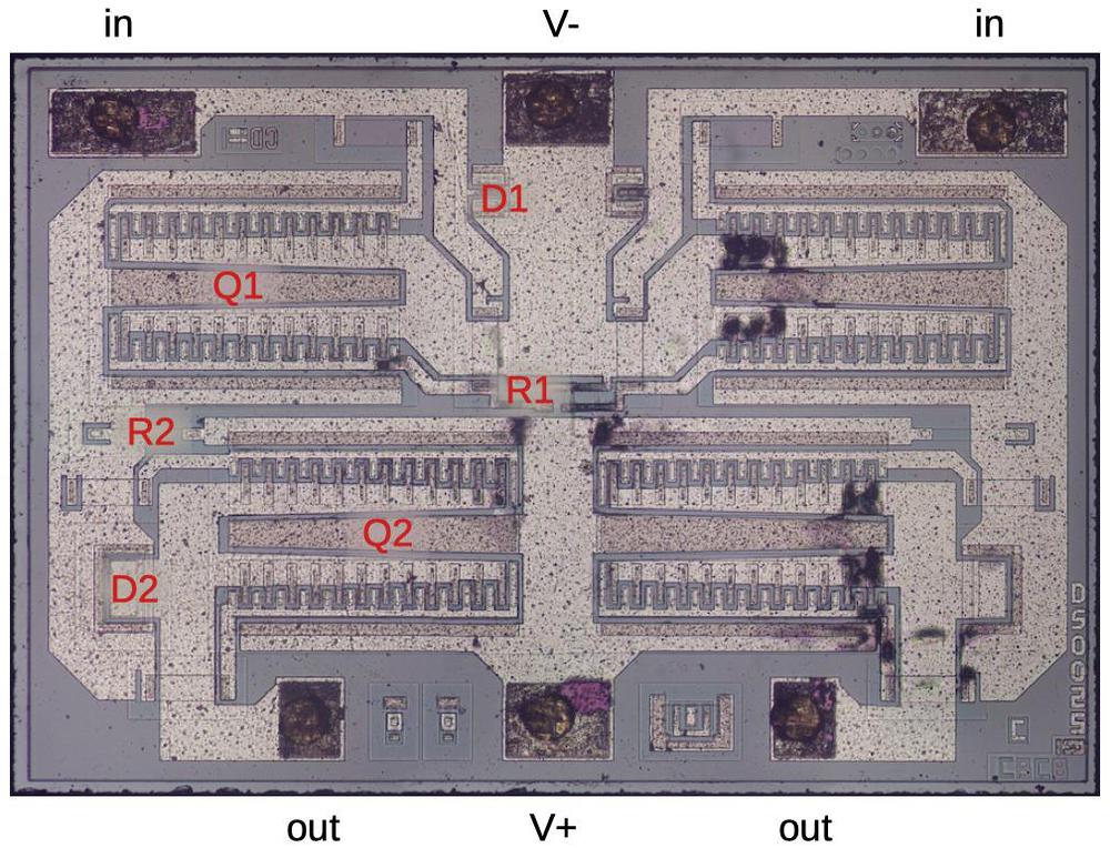
The photo above shows the silicon die under the microscope. This chip is very simple, containing four large NPN transistors, four diodes, and four resistors. The silicon appears blue-gray in this image, while the metal layer on top appears speckled white. Around the outside of the die, are six dark rectangles, the pads where golden bond wires connected the die to the chip's external pins.
The die was encased in an epoxy package. To expose the die, Eric (@TubeTimeUS) tediously sanded through the plastic package until the die was visible. Some bits of epoxy remained, caught in the bond wires, so I cleaned up the die with a few drops of boiling sulfuric acid.
The Apple-1's display
The Apple-1 displayed 24 lines of forty characters on a television monitor. Like most computers at the time, the Apple-1 stored characters rather than pixels to reduce memory requirements. A character-generation ROM converted each character into a 5×7 matrix of pixels as it was displayed. To reduce memory even more, the display didn't store full bytes, but 6-bit characters, supporting upper-case letters, numbers, and some symbols.
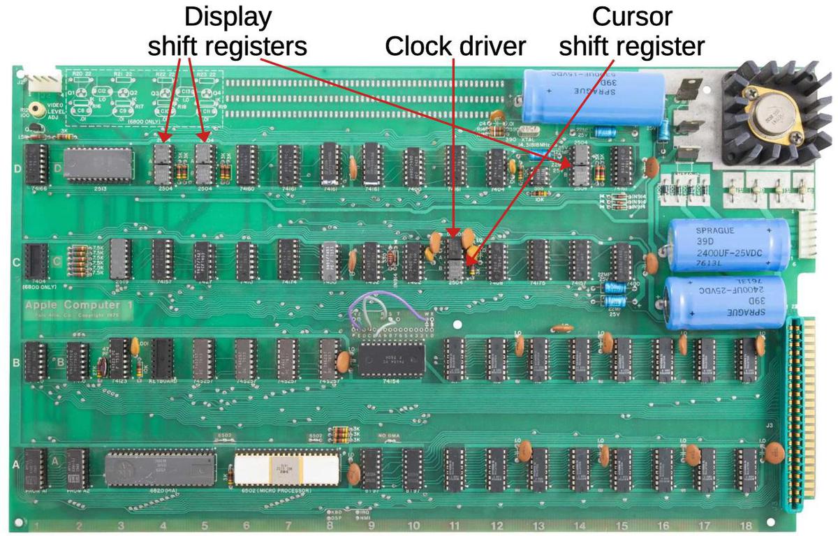
The six-bit display characters were held in six 1024-bit shift registers. A seventh shift register tracked the cursor position.3 The diagram below shows the shift registers and the clock driver on the Apple-1 circuit board. These chips are in 8-pin packages, so two chips fit into the space of a regular TTL chip.
Transistors
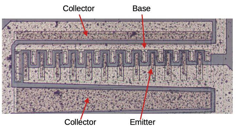
Next, I'll discuss the components of the chip. Because the chip generates high-current pulses, it uses large NPN transistors, with a different construction from most integrated circuit transistors. Each transistor consists of 24 emitters, paralleled in two groups. (You can consider it one large transistor, 2 transistors, or 24 small transistors.) The transistor is structured vertically with the collector (made of N-doped silicon) underneath, a thin P-type base in between, and the N-type emitters embedded in the top, forming the N-P-N layers of the transistor. The doped silicon regions are faintly visible with black lines around their boundaries.
In the photo above, you can see the metal wiring for the transistor's collector, base, and emitter. The collector wiring is on the outside, with base wiring in between. The collector and emitter wiring is tapered: at one end, the wiring needs to support the full current load, while at the other end it only handles 1/12 of the current. The tapered approach saves space, since it is thicker only where it needs to be thick.
Resistors
The resistors are formed from silicon doped to have higher resistance. The doped silicon rectangle is faintly visible in the die photo. At each end of the resistor, a contact connects the silicon to the metal layer on top. The 1000Ω resistor on the left is longer than the 250Ω resistor on the right, giving it more resistance.
"Tunnels"
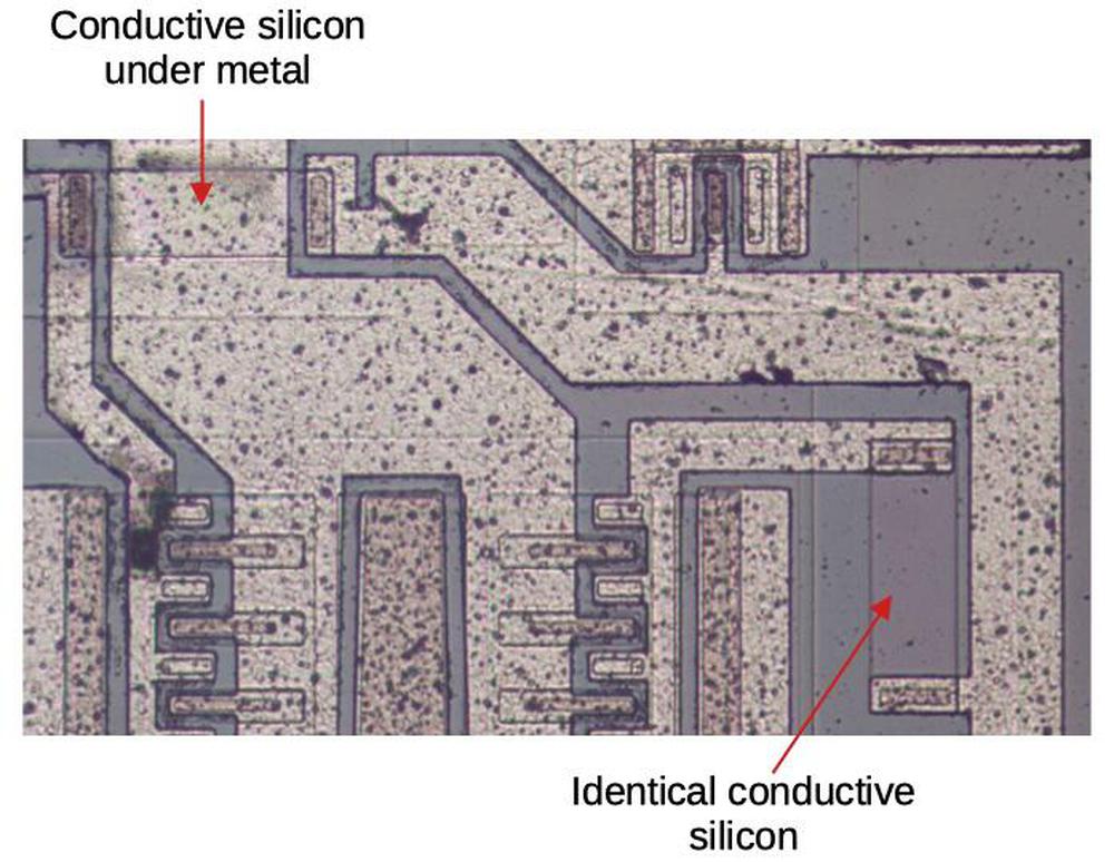
The chip has a single layer of metal wiring, which poses a problem if two signals need to cross. The solution is to put one signal in the silicon layer so it can pass under the metal layer. In essence, a low-valued resistor is used to pass under the metal layer. The image below shows how a tunnel appears on the die.
One problem is that the silicon has relatively high resistance compared to metal, so the tunnel adds resistance. The chip is carefully designed so both "sub-transistors" encounter the same resistance, to avoid one transistor turning on before the other. You can see that the input path in the upper left has a tunnel to pass under the metal wiring, while the path in the lower right has a tunnel of identical dimensions that doesn't go under any metal. While the second tunnel appears pointless, it assures that both paths have the same resistance.
The chip's circuit
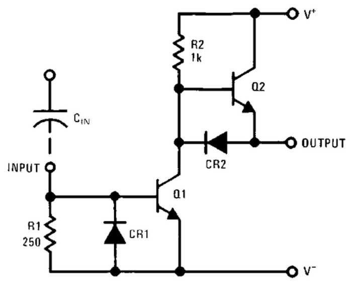
The shift register requires a two-phase clock, that is two clock signals in alternation that step the bits through the circuit. To support this, the clock driver chip has two identical driver circuits. The schematic below shows one of the circuits. When the input goes high, it turns on transistor Q1, pulling its collector low. This pulls the output low through diode CR2. When the input drops, Q1 turns off. This lets R2 provide a current to the base of Q2, turning it on, and pulling the output high. Thus, the circuit is essentially an inverter, but one that can provide up to 1.5 amps of output.4
The image below shows the various components of the schematic as they appear on the die. Most of the chip is occupied by the large power transistors. Although the chip is mounted in an 8-pin package, only six pins are used; the corresponding pads are labeled below. The chip consists of two identical mirror-image drivers; one is labeled. There are a few blackened regions in the transistors; we suspect this is where the chip failed.
Conclusion
This chip provides an interesting view of computer technology in the 1970s. The Apple-1 used shift-register memory, a technology that rapidly became obsolete as RAM prices dropped. Shift-register memory required a specialized clock driver integrated circuit, a chip that contained just four large transistors. With billions of transistors in modern integrated circuits, it's hard to imagine that it was once worthwhile to build a chip that was this simple. The Apple II, introduced just a year later in 1977, used RAM chips for all its storage, making shift-register memory a thing of the past.
I announce my latest blog posts on Twitter, so follow me @kenshirriff. I also have an RSS feed. Thanks to @TubeTimeUS for supplying the chip. I've written about the Intel 1405 shift register memory if you want to know more about this type of storage.
Notes and references
-
Looking in an old Byte magazine from 1976, a 1-kilobit shift register chip cost $9 ($34 in current dollars), while a 4-kilobit DRAM chip cost $20 ($75 in current dollars). Thus, it appears that even by the time the Apple-1 was released, DRAMs had become cheaper than shift registers. (This also illustrates the amazing drop in memory prices since the 1970s, as described by Moore's Law.)
The Apple-1 used 4-kilobit RAM for data and program storage. It's possible, though, to build a computer that uses shift-register storage for its main memory. The Datapoint 2200 is one example. If memory is accessed sequentially, shift-register storage is efficient since the bits are provided sequentially. However, if you access memory out of sequence, the processor has to wait while the memory cycles around, until the desired bits become available. In a way, shift-register memory is a throwback to very early computers such as EDSAC(1949), which used mercury delay lines for main storage. ↩
-
The IBM 2260 video display terminal (1965) used a technique similar to shift registers: it stored data in a sonic delay line, sending torsional pulses through a 50-foot nickel wire. But unlike the Apple-1, this delay line stored pixels, not characters. For more about this system, see my blog post. ↩
-
The display circuitry has some additional complexity. Characters can't be taken directly from the display shift register: since each character is made up of eight scan lines; a line of character must be processed eight times. To handle this, a second shift register (six 40-bit registers) buffers a line of characters and feeds each character into a display ROM. Another 1024-bit shift register keeps track of the cursor position. For more details, see this post. The Apple-1 schematic is in the Operation Manual. ↩
-
The large current is required because of the design of the shift-register memory. The clock line snakes through the chip, providing a clock signal to each stage of the shift register. As a result, the clock line has a fairly high capacitance, about 150 picofarads. This clock line must be switched between +5 volts and -11 volts at a 1 megahertz rate. The combination of large capacitance and large voltage swing with the fast rate requires a high current. ↩

12 comments:
Good history!!
I love this.
I'd like to point out that the HP-35 calculator, introduced in 1972, also employed dynamic shift register memory implemented in PMOS. HP designed a custom clock driver chip that's described in the HP patent, US 4,001,569, and is clearly explained in the late Jacques Laporte's excellent website here: https://archived.hpcalc.org/laporte/CLOCK-DRIVER.htm. I assume Steve Wozniak (the Apple-1's designer) would have known about that.
Thanks for another fascinating deep dive into tech history.
-Rob
This is really cool. I appreciate that you explain so well how they jumper signals across the silicon.
In the schematic of the circuit, the diodes are labeled CR1 and CR2, but you refer to them a D1 and D2, correct? It made my brain stumble a bit when I first, and then I wondered why you didn't consistently use the same terminology as the (I think outdated) schematic, or at least a quick note explaining it.
Is the CR# an older style schematic reference standard? The Q# for transistors and R# for resisters matches current (sorry!) standards, I think.
@JohnS According to the Wikipedia page, CR stands for "crystal rectifier" and is sometimes used.
John: yes, the diodes are labeled CR in the schematic but D in the diagram. Apologies for the confusion. I've added a note to the diagram. Thanks, Clonkex, for the explanation above.
Ken,
Thanks for your update! I really enjoy (but don't always understand!) the information you provide, and I keep learning new things all the time.
Ken,
I must be stupid, but I don't see any update or note about the diagram in the section starting with "The chip's circuit" to explaine the CR# is really D# in today's useage. Feel free to nuke my comments if need be! :-)
I put a note in the caption for the die image, but you're right, I should explain in the text too.
On note 1:
First idea was Apple 1 to use SRAM in order to avoid circuit for DRAM refresh.
Thank for for writing this. I had long assumed that the Apple-1 was merely an Apple II with less DRAM and a simpler display generator. I never bothered to look for a schematic. Needless to say, I enjoyed reading this article to learn the details. It is great learn these extra little steps in the evolution of computers, and I appreciate your continuing efforts.
Woz really is a genius! and a beautiful guy all around. I'm a fan of his, can't you tell? :/ I don't know how Woz put up with Jobs, they are so un-alike. Thank you for showing us this wonderful example of engineering, it's really top-notch.
Post a Comment