In 1978, Intel introduced the 8086 processor, a revolutionary chip that led to the modern x86 architecture. Unlike modern 64-bit processors, however, the 8086 is a 16-bit chip. Its arithmetic/logic unit (ALU) operates on 16-bit values, performing arithmetic operations such as addition and subtraction, as well as logic operations including bitwise AND, OR, and XOR. The 8086's ALU is a complicated part of the chip, performing 28 operations in total.1
In this post, I discuss the circuitry that controls the ALU, generating the appropriate control signals for a particular operation. The process is more complicated than you might expect. First, a machine code instruction results in the execution of multiple microcode instructions. Using the ALU is a two-step process: one microcode instruction (micro-instruction) configures the ALU for the desired operation, while a second micro-instruction gets the results from the ALU. Moreover, based on both the microcode micro-instruction and the machine code instruction, the control circuitry sends control signals to the ALU, reconfiguring it for the desired operation. Thus, this circuitry provides the "glue" between the micro-instructions and the ALU.
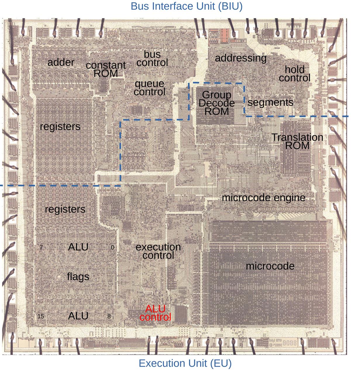
The die photo below shows the 8086 processor under a microscope. I've labeled the key functional blocks. Architecturally, the chip is partitioned into a Bus Interface Unit (BIU) at the top and an Execution Unit (EU) below. The BIU handles bus and memory activity as well as instruction prefetching, while the Execution Unit (EU) executes the instructions. In the lower right corner, the microcode ROM holds the micro-instructions. The ALU is in the lower left corner, with bits 7-0 above and bits 15-8 below, sandwiching the status flag circuitry. The ALU control circuitry, highlighted in red at the bottom of the chip, is the focus of this article.
Microcode
The 8086 processor implements most machine instructions in microcode, with a micro-instruction for each step of the machine instruction. (I discuss the 8086's microcode in detail here.) The 8086 uses an interesting architecture for microcode: each micro-instruction performs two unrelated operations. The first operation moves data between a source and a destination. The second operation can range from a jump or subroutine call to a memory read/write or an ALU operation. An ALU operation has a five-bit field to specify a particular operation and a two-bit field to specify which temporary register provides the input. As you'll see below, these two fields play an important role in the ALU circuitry.
In many cases, the 8086's micro-instruction doesn't specify the ALU operation, leaving the details to be substituted from the machine instruction opcode. For instance, the ADD, SUB, ADC, SBB, AND, OR, XOR, and CMP machine instructions share the same microcode, while the hardware selects the ALU operation from the instruction opcode. Likewise, the increment and decrement instructions use the same microcode, as do the decimal adjust instructions DAA and DAS, and the ASCII adjust instructions AAA and AAS. Inside the micro-instruction, all these operations are performed with a "pseudo" ALU operation called XI (for some reason). If the microcode specifies an XI ALU operation, the hardware replaces it with the ALU operation specified in the instruction. Another important feature of the microcode is that you need to perform one ALU micro-instruction to configure the ALU's operation, but the result isn't available until a later micro-instruction, which moves the result to a destination. This has the consequence that the hardware must remember the ALU operation.
To make this concrete, here is the microcode that implements a typical arithmetic instruction such as ADD AL, BL or XOR [BX+DI], CX.
This microcode consists of three micro-instructions.
The left half of each micro-instruction specifies a data movement, first moving the two arguments to ALU temporary registers
and then storing the ALU result (called Σ).
The right half of each micro-instruction performs the second task.
First, the ALU is configured to perform an XI operation using temporary register A. Recall that XI indicates the ALU operation
is filled in from the machine instruction; this is how the same microcode handles eight different types of machine instructions.
In the second micro-instruction, the next machine instruction is started unless a memory writeback is required (WB).
The last micro-instruction is RNI (Run Next Instruction) to start a new machine instruction. It also indicates that the
processor status flags (F) should be updated to indicate if the ALU result is zero, positive, overflow, and so forth.2
M → tmpa   XI   tmpa  Load first argument, configure ALU.
R → tmpb   WB,NXT     Load second argument, start Next instruction if no memory writeback
Σ → M      RNI  F     Store ALU result, Run Next Instruction, update status Flags
The ALU circuit
The ALU is the heart of a processor, performing arithmetic and logic operations. Microprocessors of the 1970s typically supported addition and subtraction; logical AND, OR, and XOR; and various bit shift operations. (Although the 8086 had multiply and divide instructions, these were implemented in microcode, not in the ALU.) Since an ALU is both large and critical to performance, chip architects try to optimize its design. As a result, different microprocessors have widely different ALU designs. For instance, the 6502 microprocessor has separate circuits for addition and each logic operation; a multiplexer selects the appropriate output. The Intel 8085, on the other hand, uses an optimized clump of gates that performs the desired operation based on control signals (details), while the Z80's 4-bit ALU uses a different clump of gates (details).
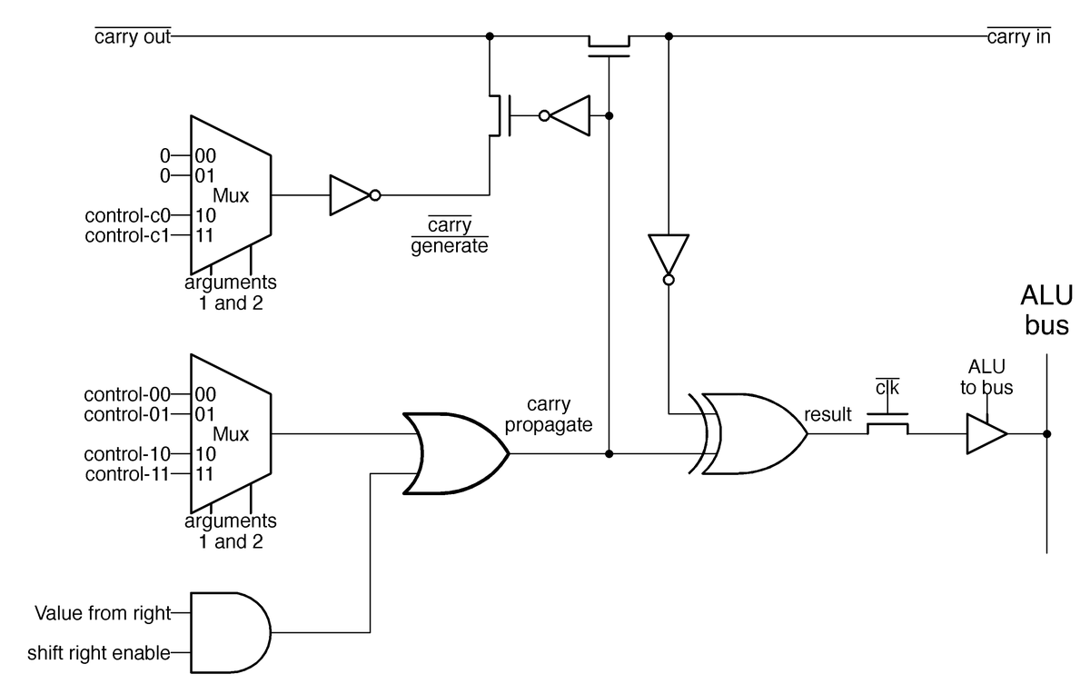
The 8086 takes a different approach, using two lookup tables (along with other gates) to generate the carry and output signals for each bit in the ALU. By setting the lookup tables appropriately, the ALU can be configured to perform the desired operation. (This is similar to how an FPGA implements arbitrary functions through lookup tables.) The schematic below shows the circuit for one bit of the ALU. I won't explain this circuit in detail since I explained it in an earlier article.3 The relevant part of this circuit is the six control signals at the left. The two multiplexers (trapezoidal symbols) implement the lookup tables by using the two input argument bits to select outputs from the control signals to control carry generation and carry propagation. Thus, by feeding appropriate control signals into the ALU, the 8086 can reconfigure the ALU to perform the desired operation. For instance, with one set of control signals, this circuit will add. Other sets of control signals will cause the circuit to subtract or compute a logical operation, such as AND or XOR. The 8086 has 16 copies of this circuit, so it operates on 16-bit values.
The 8086 is a complicated processor, and its instructions have many special cases, so controlling the ALU is more complex than described above. For instance, the compare operation is the same as a subtraction, except the numerical result of a compare is discarded; just the status flags are updated. The add versus add-with-carry instructions require different values for the carry into bit 0, while subtraction requires the carry flag to be inverted since it is treated as a borrow. The 8086's ALU supports increment and decrement operations, but also increment and decrement by 2, which requires an increment signal into bit 1 instead of bit 0. The bit-shift operations all require special treatment. For instance, a rotate can use the carry bit or exclude the carry bit, while and arithmetic shift right requires the top bit to be duplicated. As a result, along with the six lookup table (LUT) control signals, the ALU also requires numerous control signals to adjust its behavior for specific instructions. In the next section, I'll explain how these control signals are generated.
ALU control circuitry on the die
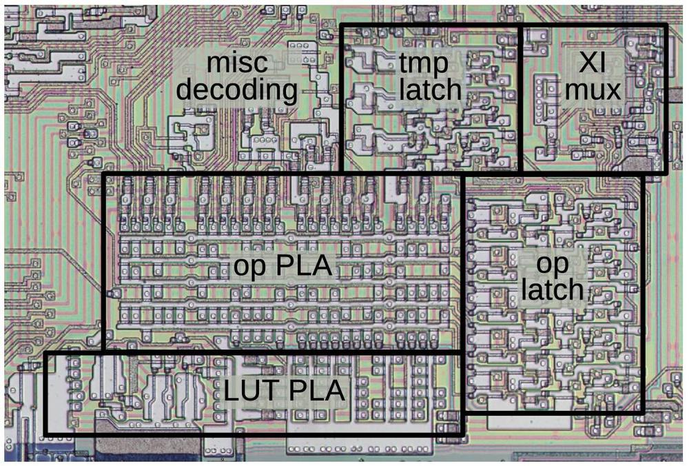
The diagram below shows the components of the ALU control logic as they appear on the die. The information from the micro-instruction enters at the right and is stored in the latches. The PLAs (Programmable Logic Arrays) decode the instruction and generate the control signals. These signals flow to the left, where they control the ALU.
As explained earlier, if the microcode specifies the XI operation, the operation field is replaced with a value based on the machine instruction opcode.
This substitution is performed by the XI multiplexer before the value is stored in the operation latch.
Because of the complexity of the 8086 instruction set, the XI operation is not as straightforward as you might expect.
This multiplexer gets three instruction bits from a special register called the "X" register, another instruction bit from the instruction
register, and the final bit from a decoding circuit called the Group Decode ROM.4
Recall that one micro-instruction specifies the ALU operation, and a later micro-instruction accesses the result. Thus, the ALU control circuitry must remember the specified operation so it can be used later. In particular, the control circuitry must keep track of the ALU operation to perform and the temporary register specified. The control circuitry uses three flip-flops to keep track of the specified temporary register, one flip-flop for each register. The micro-instruction contains a two-bit field that specifies the temporary register. The control circuitry decodes this field and activates the associated flip-flop. The outputs from these flip-flops go to the ALU and enable the associated temporary register. At the start of each machine instruction,5 the flip-flops are reset, so temporary register A is selected by default.
The control circuitry uses five flip-flops to store the five-bit operation field from the micro-instruction. At the start of each machine instruction, the flip-flops are reset so operation 0 (ADD) is specified by default. One important consequence is that an add operation can potentially be performed without a micro-instruction to configure the ALU, shortening the microcode by one micro-instruction and thus shortening the instruction time by one cycle.
The five-bit output from the operation flip-flops goes to the operation PLA (Programmable Logic Array)7, which decodes the operation into 27 control signals.6 Many of these signals go to the ALU, where they control the behavior of the ALU for special cases. About 15 of these signals go to the Lookup Table (LUT) PLA, which generates the six lookup table signals for the ALU. At the left side of the LUT PLA, special high-current driver circuits amplify the control signals before they are sent to the ALU. Details on these drivers are in the footnotes.8
Conclusions
Whenever I look at the circuitry of the 8086 processor, I see the differences between a RISC chip and a CISC chip. In a RISC (Reduced Instruction Set Computer) processor such as ARM, instruction decoding is straightforward, as is the processor circuitry. But in the 8086, a CISC (Complex Instruction Set Computer) processor, there are corner cases and complications everywhere. For instance, an 8086 machine instruction sometimes specifies the ALU operation in the first byte and sometimes in the second byte, and sometimes elsewhere, so the X register latch, the XI multiplexer, and the Group Decode ROM are needed. The 8086's ALU includes obscure operations including four types of BCD adjustments and seven types of shifts, making the ALU more complicated. Of course, the continuing success of x86 shows that this complexity also has benefits.
This article has been a deep dive into the details of the 8086's ALU, but I hope you have found it interesting. If it's too much detail for you, you might prefer my overview of the 8086 ALU.
For updates, follow me on Bluesky (@righto.com), Mastodon (@[email protected]), or RSS.
Credits: Thanks to Marcin Peczarski for discussion. My microcode analysis is based on Andrew Jenner's 8086 microcode disassembly.
Notes and references
-
The operations implemented by the ALU are:
00 ADD Add 01 OR Logical OR 02 ADC Add with carry in 03 SBB Subtract with borrow in 04 AND Logical AND 05 SUBT Subtract 06 XOR Logical XOR 07 CMP Comparison 08 ROL Rotate left 09 ROR Rotate right 0a LRCY Left rotate through carry 0b RRCY Right rotate through carry 0c SHL Shift left 0d SHR Shift right 0e SETMO Set to minus one (questionable) 0f SAR Arithmetic shift right 10 PASS Pass argument unchanged 11 XI Instruction specifies ALU op 14 DAA Decimal adjust after addition 15 DAS Decimal adjust after subtraction 16 AAA ASCII adjust after addition 17 AAS ASCII adjust after subtraction 18 INC Increment 19 DEC Decrement 1a COM1 1's complement 1b NEG Negate 1c INC2 Increment by 2 1d DEC2 Decrement by 2 -
You might wonder how this microcode handles the 8086's complicated addressing modes such as
[BX+DI]. The trick is that microcode subroutines implement the addressing modes. For details, see my article on 8086 addressing microcode. ↩ -
The 8086's ALU has a separate circuit to implement shift-right. The problem is that data in an ALU normally flows right-to-left as carries flow from lower bits to higher bits. Shifting data to the right goes against this direction, so it requires a special path. (Shifting to the left is straightforward; you can add a number to itself.)
The adjust operations (DAA, DAS, AAA, AAS) also use completely separate circuitry. These operations generate correction factors for BCD (binary-coded decimal) arithmetic based on the value and flags. The circuitry for these operations is located with the flags circuitry, separate from the rest of the ALU circuitry. ↩
-
In more detail, the 8086 stores bits 5-3 of the machine instruction in the "X" register. For an XI operation, the X register bits become bits 2-0 of the ALU operation specification, while bit 3 comes from bit 6 of the instruction, and bit 4 comes from the Group Decode ROM for certain instructions. The point of this is that the instruction set is designed so bits of the instruction correspond to bits of the ALU operation specifier, but the mapping is more complicated than you might expect. The eight basic arithmetic/logic operations (ADD, SUB, OR, etc) have a straightforward mapping that is visible from the 8086 opcode table, but the mapping for other instructions isn't as obvious. Moreover, sometimes the operation is specified in the first byte of the machine instruction, but sometimes it is specified in the second byte, which is why the X register needs to store the relevant bits. ↩
-
The flip-flops are reset by a signal in the 8086, called "Second Clock". When a new machine instruction is started, the "First Clock" signal is generated on the instruction's first byte and the "Second Clock" signal is generated on the instruction's second byte. (Note that these signals are not necessarily on consecutive clock cycles, because a memory fetch may be required if the instruction queue is empty.) Why are the flip-flops reset on Second Clock and not First Clock? The 8086 has a small degree of pipelining, so the previous micro-instruction may still be finishing up during First Clock of the next instruction. By Second Clock, it is safe to reset the ALU state. ↩
-
For reference, the 27 outputs from the PLA are triggered by the following ALU micro-operations:
Output 0: RRCY (right rotate through carry)
Output 1: ROR (Rotate Right)
Output 2: BCD Adjustments: DAA (Decimal Adjust after Addition), DAS (Decimal Adjust after Subtraction), AAA (ASCII Adjust after Subtraction), or AAS (ASCII Adjust after Subtraction)
Output 3: SAR (Shift Arithmetic Right)
Output 4: Left shift: ROL (Rotate Left), RCL (Rotate through Carry Left), SHL (Shift Left), or SETMO (Set Minus One)
Output 5: Right shift: ROR (Rotate Right), RCR (Rotate through Carry Right), SHR (Shift Right), or SAR (Shift Arithmetic Right)
Output 6: INC2 (increment by 2)
Output 7: ROL (Rotate Left)
Output 8: RCL (Rotate through Carry Left)
Output 9: ADC (add with carry)
Output 10: DEC2 (decrement by 2)
Output 11: INC (increment)
Output 12: NEG (negate)
Output 13: ALU operation 12 (unused?)
Output 14: SUB (Subtract), CMP (Compare), DAS (Decimal Adjust after Subtraction), AAS (ASCII Adjust after Subtraction)
Output 15: SBB (Subtract with Borrow)
Output 16: ROL (Rotate Left) or RCL (Rotate through Carry Left)
Output 17: ADD or ADC (Add with Carry)
Output 18: DEC or DEC2 (Decrement by 1 or 2)
Output 19: PASS (pass-through) or INC (Increment)
Output 20: COM1 (1's Complement) or NEG (Negate)
Output 21: XOR
Output 22: OR
Output 23: AND
Output 24: SHL (Shift Left)
Output 25: DAA or AAA (Decimal/ASCII Adjust after Addition)
Output 26: CMP (Compare) ↩ -
A Programmable Logic Array is a way of implementing logic gates in a structured grid. PLAs are often used in microprocessors because they provide a dense way of implementing logic. A PLA normally consists of two layers: an "OR" layer and an "AND" layer. Together, the layers produce "sum-of-products" outputs, consisting of multiple terms OR'd together. The ALU's PLA is a bit unusual because many outputs are taken directly from the OR layer, while only about 15 outputs from the first layer are fed into the second layer. ↩
-
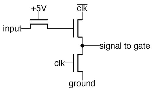
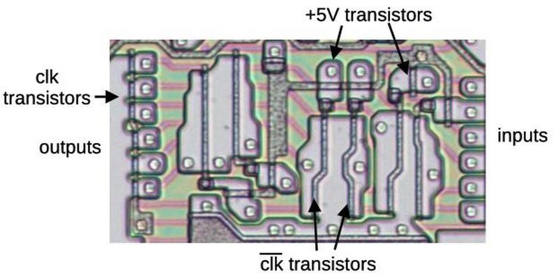
The control signals pass through the driver circuit below. The operation of this circuit puzzled me for years, since the transistor with its gate at +5V seems to be stuck on. But I was looking at the book DRAM Circuit Design and spotted the same circuit, called the "Bootstrap Wordline Driver". The purpose of this circuit is to boost the output to a higher voltage than a regular NMOS circuit, providing better performance. The problem with NMOS circuitry is that NMOS transistors aren't very good at pulling a signal high: due to the properties of the transistor, the output voltage is less than the gate voltage, lower by the threshold voltage VTH, half a volt or more.
The drive signals to the ALU gates are generated with this dynamic circuit.The bootstrap circuit takes advantage of capacitance to get more voltage out of the circuit. Specifically, suppose the input is +5V, while the clock is high. Point A will be about 4.5V, losing half a volt due to the threshold. Now, suppose the clock goes low, so the inverted clock driving the upper transistor goes high. Due to capacitance in the second transistor, as the source and drain go high, the gate will be pulled above its previous voltage, maybe gaining a couple of volts. The high voltage on the gate produces a full-voltage output, avoiding the drop due to VTH. But why the transistor with its gate at +5V? This transistor acts somewhat like a diode, preventing the boosted voltage from flowing backward through the input and dissipating.
The bootstrap circuit is used on the ALU's lookup table control signals for two reasons. First, these control signals drive pass transistors. A pass transistor suffers from a voltage drop due to the threshold voltage, so you want to start with a control signal with as high a voltage as possible. Second, each control signal is connected to 16 transistors (one for each bit). This is a large number of transistors to drive from one signal, since each transistor has gate capacitance. Increasing the voltage helps overcome the R-C (resistor-capacitor) delay, improving performance.
A close-up of the bootstrap drive circuits, in the left half of the LUT PLA.The diagram above shows six bootstrap drivers on the die. At the left are the transistors that ground the signals when clock is high. The +5V transistors are scattered around the image; two of them are labeled. The six large transistors provide the output signal, controlled by clock'. Note that these transistors are much larger than the other transistors because they must produce the high-current output, while the other transistors have more of a supporting role.
(Bootstrap circuits go way back; Federico Faggin designed a bootstrap circuit for the Intel 8008 that he claimed "proved essential to the microprocessor realization.") ↩
7 comments:
The full die photo shows the 8088, not the 8086 as written. The overall layout of the functional blocks is still the same of course, so no big deal... just a heads-up.
Thanks, VileR. I don't know how I mixed up the die images. I've updated with the correct die.
> The 8086 uses an interesting architecture for microcode: each micro-instruction performs two unrelated operations.
Is this a slight hint of VLIW? Where "very long" stands for "just two". Intel was very intimate with VLIW both before and after 8086. Or is this just a common way of designing microcoded CPU cores?
Can anyone point me in the direction of similar work on the first ARM architecture, over here in the UK that was a very important design. Its a story that is little known in the US despite ARMs now massively out numbering everything else, 300 Billion produced.
Fascinating as usual, but with deference I reckon you meant to type ALU not CPU here: “the Z80's 4-bit CPU” - most of us owe you the fascinating insight that Z80s chomp nybbles internally, of course. But it’s surely too late to reclassify the CPU itself, and if so where does that leave the 8080? 😄
Where you say “the Z80's 4-bit CPU”, do you mean ALU?
To Ken Shirriff
Have you ever seen these before? I haven't.
https://m.facebook.com/groups/1082975419579024/permalink/1745167016693191/?ref=share&mibextid=NOb6eG
Post a Comment