Interrupts have been an important part of computers since the mid-1950s,1 providing a mechanism to interrupt a program's execution. Interrupts allows the computer to handle time-critical tasks such as I/O device operations. In this blog post, I look at the interrupt features in the Intel 8086 (1978) and how they are implemented in silicon, a combination of interesting circuitry and microcode.
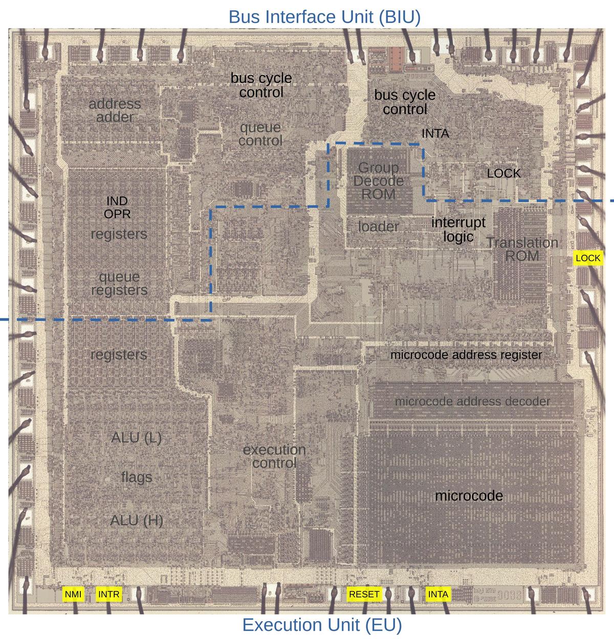
I've been reverse-engineering the 8086 starting with the silicon die. The die photo below shows the chip under a microscope. The metal layer on top of the chip is visible, with the silicon and polysilicon mostly hidden underneath. Around the edges of the die, bond wires connect pads to the chip's 40 external pins; relevant pins are marked in yellow. I've labeled the key functional blocks; the ones that are important to this discussion are darker and will be discussed in detail below. Architecturally, the chip is partitioned into a Bus Interface Unit (BIU) at the top and an Execution Unit (EU) below. The BIU handles bus activity, while the Execution Unit (EU) executes instructions and microcode. Both parts are extensively involved in interrupt handling.
Interrupts in the 8086
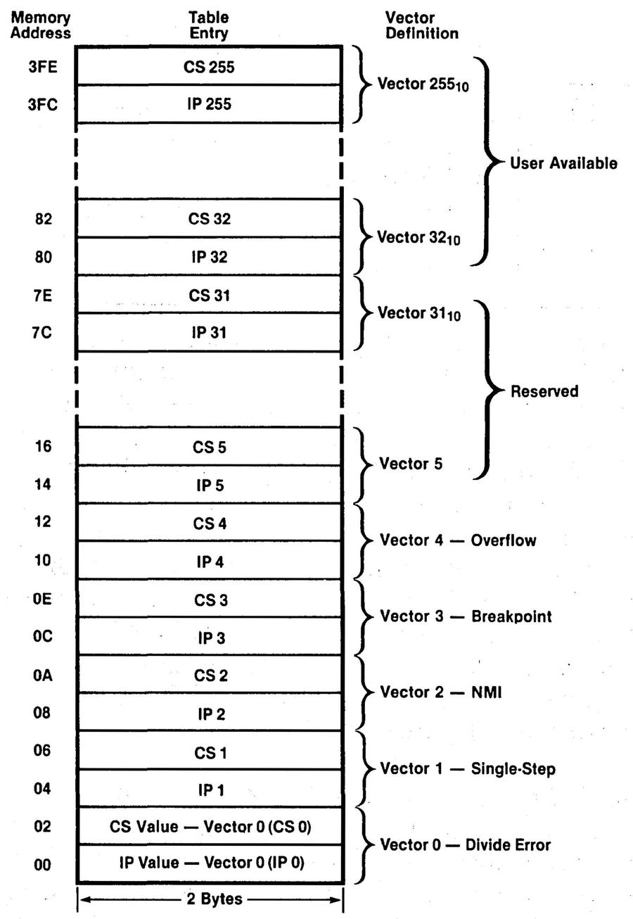
The idea behind an interrupt is to stop the current flow of execution, run an interrupt handler to perform a task, and then continue execution where it left off. An interrupt is like a subroutine call in some ways; it pushes the current segment register and program counter on the stack and continues at a new address. However, there are a few important differences. First, the address of the interrupt handler is obtained indirectly, through an interrupt vector table. Interrupts are numbered 0 through 255, and each interrupt has an entry in the vector table that gives the address of the code to handle the interrupt. Second, an interrupt pushes the processor flags to the stack, so they can be restored after the interrupt. Finally, an interrupt clears the interrupt and trap flags, blocking more interrupts while handling the interrupt.
The 8086 provides several types of interrupts, some generated by hardware and some generated by software. For hardware interrupts, the INTR pin on the chip generates a maskable interrupt when activated, while the NMI pin on the chip generates a higher-priority non-maskable interrupt.2 Typically, most interrupts use the INTR pin, signaling things such as a timer, keyboard request, real-time clock, or a disk needing service. The NMI interrupt is designed for things such as parity error or an impending power failure, which are so critical they can't be delayed. The 8086 also has a RESET pin that resets the CPU. Although not technically an interrupt, the RESET action has many features in common with interrupts, so I'll discuss it here.
On the software side, the 8086 has multiple types of interrupts generated by different instructions.
The INT n instruction creates an interrupt of the specified type (0 to 255).
These software interrupts were used in the IBM PC to execute a function in the BIOS, the layer underneath the operating system.
These functions could be everything from a floppy disk operation to accessing the printer.
The one-byte INT 3 instruction creates a breakpoint interrupt for debugging.
The divide instructions generate an interrupt if a divide-by-zero or overflow occurs.
The INTO instruction (Interrupt if Overflow) generates an interrupt
if the overflow flag is set.
To support single-step mode in debuggers, the Trap flag generate an interrupt on every instruction.
The diagram below shows how the vector table is implemented. Each of the 256 interrupt types has an entry holding the address of the interrupt handler (the code segment value and the instruction pointer (program counter) value). In the next section, I'll show below how the microcode loads the vector from the table and switches execution to that interrupt handler.
Microcode
Most of the operations in the 8086 are implemented in microcode, a low-level layer of code that sits between the machine code instructions and the chip's hardware. I'll explain a few features of the 8086's microcode that are important for the interrupt code. Each micro-instruction is 21 bits long, as shown below. The first part of the micro-instruction specifies a move between a source register and a destination register; these may be special-purpose internal registers, not just the registers visible to the programmer. The meaning of the remaining bits depends on the type of micro-instruction, but includes jumps within the microcode, ALU (Arithmetic/Logic Unit) operations, and memory operations.
For a memory access, microcode issues a memory read or write micro-instruction.
Memory accesses use two internal registers: the IND (Indirect) register holds the address in the segment,
while the OPR (Operand) register holds the word that is read or written.
A micro-instruction such as W SS,P2 writes the OPR register to the memory address specified by the IND register
and the segment register (SS indicates the stack segment). The IND register can also be incremented or decremented
(P2 indicates "Plus 2").
The 8086's Bus Interface Unit (BIU) handles the memory request in hardware, while the microcode waits.
The BIU has an adder to combine the segment address and the offset to obtain the "absolute" address.
It also has a constant ROM to increment or decrement the IND register.
Memory accesses are complicated in the 8086 and take at least four clock cycles,3 called T1, T2,
T3, and T4.
An interrupt acknowledge is almost the same as a memory read, except the IAK bit is set in the microcode,
causing some behavior changes.
The interaction between microcode and the ALU (Arithmetic/Logic Unit) will also be important.
The ALU has three temporary registers that hold the arguments for operations, called temporary A, B, and C.
These registers are invisible to the programmer.
The first argument for, say, an addition can come from any of the three registers, while the second argument is
always from the temporary B register.
Performing an ALU operation takes at least two micro-instructions. First, the ALU is configured to perform
an operation, for example, ADD or DEC2 (decrement by 2).
The result is then read from the ALU, denoted as the Σ register.
Software interrupts
The main microcode for interrupt handling is shown below.4
Each line specifies a move operation and an action, with my comments in green.
On entry to INTR interrupt handler, the OPR operand register holds the interrupt type.
This chunk of microcode looks up the interrupt handler in the vector table, pushes the status flags onto the stack,
and then branches to a routine FARCALL2 to perform a subroutine call the interrupt handler.
       move            action
19d  OPR → tmpBL     SUSP         INTR: OPR to tmpB(low), suspend prefetch
19e  0 → tmpbH       ADD tmpB      0 to tmpB(high), add tmpB to tmpB
19f  Σ → tmpB                      ALU sum to tmpB, add tmpB to tmpB
1a0  Σ → IND         R S0,P2       ALU sum to IND, read from memory, IND+=2
1a1  OPR → tmpB      DEC2 tmpC     memory to tmpB, set up decrement tmpC
1a2  SP → tmpC       R S0,P0       SP to tmpC, read from memory
1a3  OPR → tmpA                    memory to tmpA
1a4  F → OPR         CITF          Flags to OPR, clear interrupt and trap flags
1a5  Σ → IND         W SS,P0       ALU dec to IND, Write to memory
1a6  IND → tmpC      JMP FARCALL2  IND to tmpC, branch to FARCALL2
In more detail, the microcode routine starts at 19d by moving the interrupt number from the OPR register to the
low byte of the ALU's temporary B register.
The SUSP action suspends instruction prefetching since we'll start executing instructions from a new location.
Next, line 19e zeros out the top byte of the temporary B register and tells the ALU to add temporary B to itself.
The next micro-instruction puts the ALU result (indicated by Σ) into temporary B, doubling the value.
Line 1a0 calculates another sum (doubling) from the ALU and stores it in the IND register.
In other words, the interrupt number has been multiplied by 4, yielding an address into the vector table.
The interrupt handle address is read from the vector table: R S0,P2 operation reads from memory, segment 0, and performs a "Plus 2" on the IND register.
Line 1a1
puts the result (OPR) into the temporary B register.
Line 1a2 stores the current stack pointer register into temporary C. It also performs a second read to get the
handler code segment from the vector table.
Line 1a3 stores this in the temporary A register.
Line 1a4 puts the flags (F) into the OPR register. It also clears the interrupt and trap flags (CITF), blocking further interrupts.
Line 1a5 puts the ALU result (the decremented stack pointer) into the IND register. (This ALU operation was set up back in line 1a1.)
To push the flags on the stack, W SS,P0 writes OPR to the Stack segment and does a "Plus 0" on the IND register.
Finally, line 1a6 stores the IND register (the new top-of-stack) into the temporary C register and jumps to the FARCALL2 micro-routine.5
Understanding microcode can be tricky, since it is even more low-level than machine instructions, but hopefully this discussion gives you a feel for it. Everything is broken down into very small steps, even more basic than machine instructions. Microcode is a bit like a jigsaw puzzle, carefully fit together to ensure everything is at the right place at the right time, as efficiently as possible.
Subroutine call microcode: FARCALL2
Next, I'll describe the FARCALL2 microcode.
Because of its segment registers, the 8086 has two types of calls (and jumps):
a near call is a subroutine call within the same code segment, while a far call is a subroutine call
to a different code segment.
A far call target is specified with two words: the new code segment register and the new program counter.
The FARCALL2 micro-routine performs a subroutine call to a particular segment and offset.
At entry to FARCALL2, the target code segment in temporary A, the offset is in temporary B, and the
decremented stack pointer will be provided by the ALU.
The microcode below pushes the code segment register to the stack, updates the code segment
register with the new value, and then jumps to NEARCALL to finish the subroutine call.
06c  Σ → IND      CORR        FARCALL2: ALU (IND-2) to IND, correct PC
06d  CS → OPR     W SS,M2      CS to OPR, write to memory, IND-=2
06e  tmpA → CS    PASS tmpC    tmpA to CS, ALU passthrough
06f  PC → OPR     JMP NEARCALL PC to OPR, branch to NEARCALL
For a subroutine call, the program counter is saved so execution can resume where it left off.
But because of prefetching, the program counter in the 8086 points to the next instruction to fetch,
not the next instruction to execute.
To fix this, the
CORR (Correction) micro-instruction corrects the program counter value
by subtracting the length of the prefetch queue.
Line 06c also puts the decremented stack location into IND using the ALU decrement operation set up way back at line 1a1.
Line 06d puts the code segment value (CS) into the OPR register and then writes it to the stack segment,
performing a "Minus 2" on IND. In other words, the CS register is pushed onto the stack.
Line 06e stores the new value (from temporary A) into the CS register. It also sets up the ALU to pass the value
of the temporary C register as its result.
Finally, line 06f puts the (corrected) program counter into the OPR register and jumps to the NEARCALL routine.
Subroutine call microcode: NEARCALL
The NEARCALL micro-routine does a near subroutine call, updating the program counter but not the segment register.
At entry, the target address is in temporary B, the IND register indicates the top of the stack, and OPR holds the program counter.
077  tmpB → PC    FLUSH      NEARCALL: tmpB to PC, restart prefetch
078  IND → tmpC               IND to tmpC
079  Σ → IND                  ALU to IND
07a  Σ → SP       W SS,P0 RNI ALU to SP, write PC to memory, run next instruction
Line 077 puts temporary B into the program counter. The FLUSH operation flushes the stale instructions from
the prefetch queue and starts prefetching from the new PC address.
Line 078 puts IND (i.e. the new stack pointer value) into temporary C.
Line 079 puts this value into the IND register and line 07a puts this value into the SP register.
(The ALU was configured at line 06e to pass the temporary C value unmodified.)
Line 07a pushes the PC to the stack by writing OPR (the old program counter) to the stack segment.
Finally, RNI (Run Next Instruction) ends this microcode sequence and causes the 8086 to
run the next machine instruction, the first instruction of the interrupt handler.
Starting an interrupt
The above microcode handles a generic interrupt. But there's one more piece: setting up the interrupt
type for the instruction.
For instance, the INT ib machine instruction has the interrupt type in the second byte of the opcode.
This machine instruction has the two micro-instructions below.
The microcode loads the type from the instruction prefetch queue (Q) and puts it into temporary B and then OPR.
Then it jumps to the INTR microcode discussed earlier.
1a8  Q → tmpB             INT ib: load a byte from the queue
1a9  tmpB → OPR  JMP INTR  Put the byte in OPR and jump to INTR
Several instructions require specific interrupt numbers, and the microcode uses a tricky technique to obtain these numbers.
The numbers are obtained from a special pseudo-register called CR, which is all zeros except the three low bits
come from the microcode address.6
The microcode is carefully arranged in memory so the micro-instruction is at the right address to generate the necessary value.
For instance, in the microcode below, entry point INT1 will load the number 1 into OPR, entry point INT2 will load the number 2 into OPR, and INT0 will load 0 into OPR.
Each line then jumps to the main INTR interrupt microcode.
198  CR → OPR     JMP INTR      INT1: num to OPR, branch to INTR
199  CR → OPR     JMP INTR      INT2: num to OPR, branch to INTR
...
1a7  CR → OPR     JMP INTR      INT0: num to OPR, branch to INTR
The microcode for the INT 3 and INTO (not to be confused with INT0) machine instructions has some wasted micro-instructions to ensure that the CR → OPR is at the right address.
This wastes a couple of cycles and a couple of micro-instructions.7
Return from interrupt
The IRET interrupt is used to return from interrupts.
It pops the program counter, code segment register, and flags from the stack, so execution can continue
at the point where the interrupt happened.
It calls the microcode subroutine FARRET to pop the code segment register and the PC from the stack.
(I won't go into FARRET in this post.)
Then it pops the flags from the stack, updates the Stack Pointer, and runs the next instruction.
0c8               CALL FARRET IRET: call Far Return
0c9               R SS,P2      read from stack, IND+=2
0ca  OPR → F                   mem to Flags
0cb  IND → SP     RNI          IND to stack pointer, run next instruction
External hardware interrupts
As well as software interrupts, the 8086 has hardware interrupts. The 8086 chip has pins for INTR and NMI; pulling the pin high causes a hardware interrupt. This section discusses the hardware circuitry and the microcode that handles these interrupts.
The interrupt pin circuit
The schematic below shows the input circuitry for the INTR pin; the NMI, RESET, and TEST pins use the same circuit. The function of this circuit is to clean up the input and ensure that it is synchronized with the clock. The chip's INTR pin is connected to a protection diode to drain a negative voltage to ground. Next, the signal goes through three inverters, probably to force a marginal voltage to either 0 or 1. Finally, the signal goes through an edge-triggered flip-flop to synchronize it with the clock. The flip-flop is constructed from two set-reset latches, the first gated by clk' and the second gated by clk. At the output of each stage is a "superbuffer", two transistors that produce a higher-current output than a regular inverter. This flip-flop circuit is unusual for the 8086; most flip-flops and latches are constructed from dynamic logic with pass transistors, which is much more compact. The more complicated circuitry on the INTR input probably protects against metastability and other problems that could occur with poor-quality input signals.
The interrupt logic circuitry
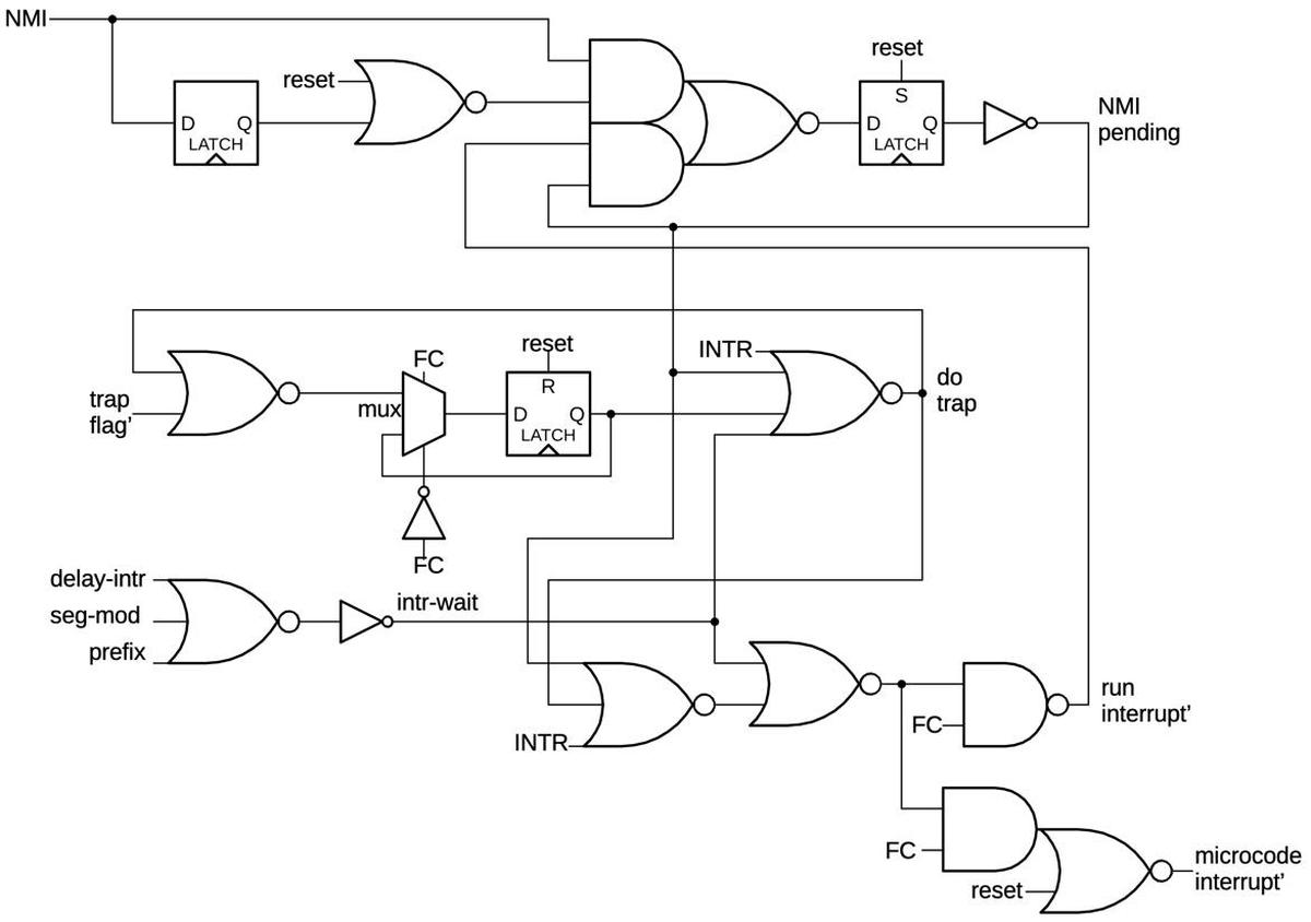
The chip has a block of interrupt logic to receive interrupts, handle interrupt priorities, and execute an interrupt at the appropriate time. This circuitry is in the top right part of the chip, on the opposite side of the chip from the interrupt pins. The schematic below shows this circuitry.
The top chunk of logic latches an NMI (non-maskable interrupt) until it runs or it is cleared by a reset.8 The first flip-flop helps convert an NMI input into a one-clock pulse. The second flip-flop holds the NMI until it runs.
The middle chunk of logic handles traps. If the trap flag is high, the latch will hold the trap request until it can take place. The latch is loaded on First Clock (FC), which indicates the start of a new instruction. The NOR gate blocks the trap if there is an interrupt or NMI, which has higher priority.9
The third chunk of logic schedules the interrupt.
Three things can delay an interrupt: an interrupt delay micro-instruction, an instruction that modifies a
segment register, or an instruction prefix.10
If not delayed, the interrupt (NMI, trap, or INTR pin) will run at the start of the next instruction (i.e. FC).11
The microcode interrupt code is run for these cases as well as a reset.
Note that the reset is not gated by First Clock, but can run at any time.
The interrupt signal from this circuitry loads a hardcoded interrupt
address into the microcode address latches, depending on the type of interrupt.12
This happens for an interrupt at First Clock, while a reset can happen any time in the instruction cycle.
A trap goes to the INT1 microcode routine described earlier, while an NMI interrupt goes to INT2 microcode routine.
The microcode for the INTR interrupt will be discussed in the next section.
The interrupt signal also goes to the Group Decode ROM (via the instruction register), where it blocks regular instruction decoding. Finally, the interrupt signal goes to a circuit called the loader, where it prevents fetching of the next instruction from the prefetch queue.
The external INTR interrupt
The INTR interrupt has some special behavior to communicate with the device that triggered the interrupt: the 8086 performs two bus cycles to acknowledge the interrupt and to obtain the interrupt number from the device. This is implemented with a combination of microcode and the bus interface logic. The bus cycles are similar to memory read cycles, but with some behavior specific to interrupts.
The INTR interrupt has its own microcode, shown below.
The first micro-instruction zeros the IND memory address register and then performs a special IAK bus cycle.13
This is similar to a memory read but asserts the INTA interrupt acknowledge line so the device knows that
its interrupt has been received.
Next, prefetching is suspended.
The third line performs a second IAK bus cycle and the external device puts the interrupt
number onto the bus. The interrupt number is read into the ORD register, just like a memory read.
At this point, the code falls through into the interrupt microcode described previously.
19a  0 → IND   IAK S0,P0  IRQ: 0 to IND, run interrupt bus cycle
19b            SUSP        suspend prefetch
19c            IAK S0,P0   run interrupt bus cycle
19d            ...        The INTR routine discussed earlier
The bus cycle
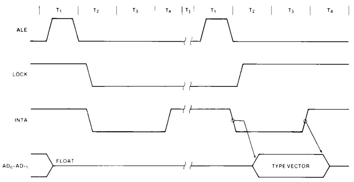
The diagram below provides timing details of the two interrupt acknowledge bus cycles. Each cycle is
similar to a memory read bus cycle, going through the T1 through T4 states, starting with an
ALE (Address Latch Enable) signal.
The main difference is the interrupt acknowledge bus cycle also raises the INTA (Interrupt Acknowledge) to
let the requesting device know that its interrupt has been acknowledged.14
On the second cycle, the device provides an 8-bit type vector that provides the interrupt number.
The 8086 also issues a LOCK signal to lock the bus from other uses during this sequence.
The point of this is that the 8086 goes through a fairly complex bus sequence when handling a hardware interrupt.
The microcode triggers these two bus cycles with the IAK micro-operation, but the bus interface circuitry
goes through the various states of the bus cycle in hardware, without involving the microcode.
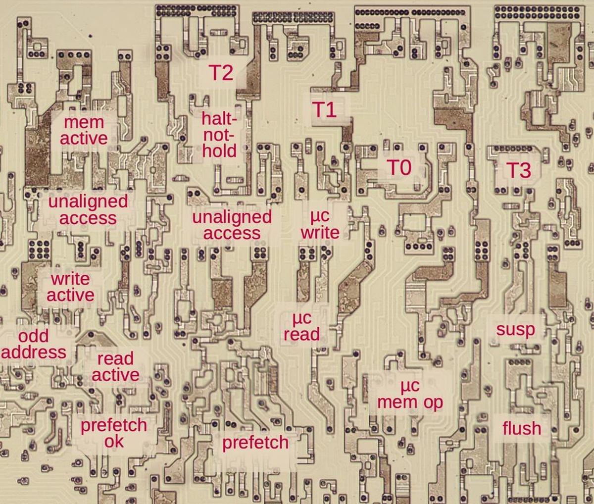
The circuitry to control the bus cycle is complicated with many flip-flops and logic gates; the diagram below shows the flip-flops. I plan to write about the bus cycle circuitry in detail later, but for now, I'll give an extremely simplified description. Internally, there is a T0 state before T1 to provide a cycle to set up the bus operation. The bus timing states are controlled by a chain of flip-flops configured like a shift register with additional logic: the output from the T0 flip-flop is connected to the input of the T1 flip-flop and likewise with T2 and T3, forming a chain. A bus cycle is started by putting a 1 into the input of the T0 flip-flop. When the CPU's clock transitions, the flip-flop latches this signal, indicating the (internal) T0 bus state. On the next clock cycle, this 1 signal goes from the T0 flip-flop to the T1 flip-flop, creating the externally-visible T1 state. Likewise, the signal passes to the T2 and T3 flip-flops in sequence, creating the bus cycle. Some special-case logic changes the behavior for an interrupt versus a read.15
Reset
The reset pin resets the CPU to an initial state. This isn't an interrupt, but much of the circuitry is the same, so I'll describe it for completeness. The reset microcode below initializes the segment registers, program counter, and flags to 0, except the code segment is initialized to 0xffff. Thus, after a reset, instruction execution will start at absolute address 0xffff0. The reset line is also connected to numerous flip-flops and circuits in the 8086 to ensure that they are initialized to the proper state. These initializations happen outside of the microcode.
1e4  0 → DS     SUSP   RESET: 0 to DS, suspend prefetch
1e5  ONES → CS          FFFF to CS
1e6  0 → PC     FLUSH   0 to PC, start prefetch
1e7  0 → F              0 to Flags
1e8  0 → ES             0 to ES
1e9  0 → SS     RNI     0 to SS, run next instruction
A bit of history
The 8086's interrupt system inherits a lot from the Intel 8008 processor.
Interrupts were a bit of an afterthought on the 8008 so the interrupt handling was primitive and designed to simplify implementation.17
In particular, an interrupt response acts like an instruction fetch except the interrupting device "jams"
an instruction on the bus.
To support this, the 8008 provided one-byte RST (Restart) instructions that would call a fixed location.
The Intel 8080 improved the 8008, but kept this model of performing an instruction fetch cycle that received a "jammed" instruction for an interrupt.
With more pins available, the 8080 added the INTA Interrupt Acknowledge pin.
The approach of "jamming" an instruction onto the bus for an interrupt is rather unusual. Other contemporary microprocessors such as the 6800, 6502, or Intel 8048 used an interrupt vector approach, which is much more standard: an interrupt vector table held pointers to the interrupt service routines.
The 8086 switched to an interrupt vector table, but retained some 8080 interrupt characteristics for backward compatibility. In particular, the 8086 performs a memory cycle very much like an instruction fetch, but instead of an instruction, it receives an interrupt number. The 8086 performs two interrupt ack bus cycles but ignores the first one, which lets the same hardware work with the 8080 and 8086.16
Conclusions
This is another blog post that I expected would be quick and easy, but there's a lot going on in the 8086's interrupt system, both in hardware and microcode. The 8086 has some strange characteristics, such as acknowledging interrupts twice, but these features make more sense when looking at the 8086's history and what it inherited from the 8008 and 8080.
I've written multiple posts on the 8086 so far and plan to continue reverse-engineering the 8086 die so follow me on Twitter @kenshirriff or RSS for updates. I've also started experimenting with Mastodon recently as @oldbytes.space@kenshirriff. Thanks to pwg on HN for suggesting interrupts as a topic.
Notes and references
-
The first computer to provide interrupts was probably the UNIVAC 1103A (1956). The book "Computer Architecture" by Blaauw and Brooks discusses different approaches to interrupts in great detail, pages 418-434. A history of interrupts is in this article. ↩
-
The maskable interrupt can be blocked in software, while the non-maskable interrupt cannot be blocked. ↩
-
A typical memory access takes four clock cycles. However, slow memory can add wait states, adding as many clock cycles as necessary. Moreover, accessing a word from an unaligned (odd) address results in two complete bus cycles to access the two bytes, since the bus can only read an aligned word at a time. Thus, memory accesses can take much more than four cycles. ↩
-
The 8086's microcode was disassembled by Andrew Jenner (link) from my die photos, so the microcode listings are based on his disassembly. ↩
-
The microcode jumps use a level of indirection because there isn't room in the micro-instruction for the full micro-address. Instead, the micro-instruction has a four-bit tag specifying the desired routine. The Translation ROM holds the corresponding micro-address for the routine, which is loaded into the microcode address register. ↩
-
The
CRtransfer source loads the low three bits of the microcode address. Its implementation is almost the same as theZEROsource, which loads zero. A signal zeroes bits 15-3 for both sources. The bottom 3 bits are pulled low for the ZERO source or if the corresponding microcode bit is 0. By the time this load happens, the microcode counter has incremented, so the value is one more than the address with the micro-instruction. Also note that it uses the raw 13-bit microcode address which is 9 bits plus four counter bits. The address decoder converts this to the 9-bit "physical" microcode address that I'm showing. The point is that the 3 lower bits from my microcode listing won't give the right value. ↩ -
The jump in the microcode is why the one-byte
INT 3instruction takes 52 clocks while the two-byteINT nninstruction takes 51 clocks. You'd expectINT nnto be slower because it has an extra byte to execute, but the microcode layout forINT 3makes it slower. ↩ -
There's a subtle difference between the NMI and the INTR interrupts. Once the NMI pin goes high, the interrupt is scheduled, even if the pin goes low. For a regular interrupt, the INTR pin must be high at the start of an instruction. Thus, NMI is latched but INTR is not. ↩
-
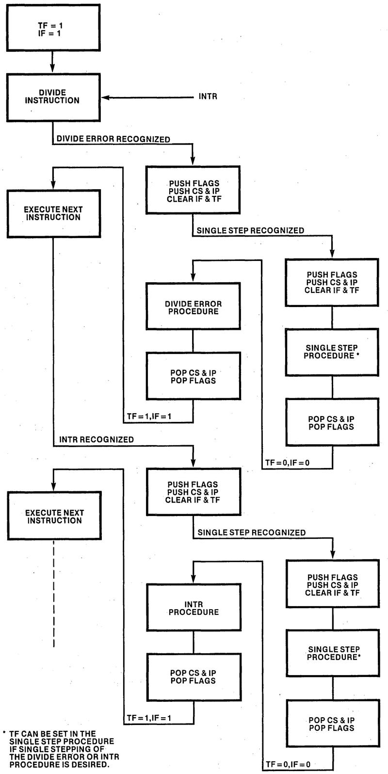
Since the 8086 has multiple interrupt sources, you might wonder how multiple interrupts are handled at the same time. The chip makes sure the interrupts are handled correctly, according to their priorities. The diagram below shows what happens if trapping (single-step) is enabled, a divide causes a divide-by-0 exception, and an external interrupt arrives.
Processing simultaneous interrupts. From iAPX 86/88 User's Manual, Figure 2-31. -
The interrupt delay micro-instruction is used for the
WAITmachine instruction. I think that a long string of prefix instructions will delay an interrupt (even an NMI) for an arbitrarily long time. ↩ -
Interrupts usually happen after the end of a machine instruction, rather than interrupting an instruction during execution. There are a couple of exceptions, however, for instructions that can take a very long time to complete (block copies) or could take forever (
WAIT). The solution is that the microcode for these instructions checks to see if an interrupt is pending, so the instruction can explicitly stop and the interrupt can be handled. ↩ -
The microcode address is 13 bits long: a special bit, 8 instruction bits, and four counter bits. For an interrupt, it is set to
1r0000000.00ab, whererindicates a reset andabindicate an interrupt of various types:
Trap: goes to vector 1, INT1 addr 198 10000000.00
NMI: goes to vector 2, INT2 addr 199 100000000.01 (Bitbis NMI)
INTR: goes to IRQ addr 19a 100000000.10, vector specified by device. Bitais intr-enable', blocked by NMI.
This logic takes into account the relative priorities of the different interrupts. This address is initialized through a special multiplexer path for interrupts that loads bits directly into the microcode address latch. ↩ -
The
IAKmicro-instruction is the same as a read micro-instruction except theIAK(Interrupt Acknowledge) bit is set. This bit controls the differences between a read micro-instruction and an interrupt acknowledge micro-instruction.The logic that makes the bus cycle an interrupt acknowledge rather than a read is a bit strange. A signal indicates that the cycle is an I/O operation or an interrupt acknowledge. This is determined by the instruction decoder (for I/O) or bit
Pof the microcode (for an interrupt acknowledge). This signal is used for the S2 status pin. Later, this signal is ANDed with the read/write signal to determine that it is an interrupt acknowledge and not an I/O. This probably optimized signal generation, but it seems inconvenient to merge two signals together and then split them out later. ↩ -
The 8086 has two different modes, giving its pins different meanings in the different modes. In "Minimum" mode, the control pins have simple functions. In particular, the interrupt is acknowledged using the INTA pin. In "Maximum" mode, the control pins are encoded to provide more state information to a bus controller. In this mode, the interrupt acknowledge state is encoded and signaled over the S2, S1, and S0 state pins. I'm discussing minimum mode; the sequence is the same in maximum mode but uses different pins. ↩
-
To prevent another device from grabbing the bus during interrupt acknowledgement, the LOCK pin is activated. The hardware for this LOCK signal toggles the internal lock latch on each of the interrupt ALE signals, so the lock is enabled on the first one and disabled on the second. The interrupt ack signal also prevents the address lines from being enabled during the interrupt ack. ↩
-
An 8086/8088 system will typically use an external chip, the 8259A Programmable Interrupt Controller. This chip extends the interrupt functionality of the 8086 by providing 8 priority-based hardware interrupts.
The Intel 8259A Programmable Interrupt Controller chip was designed to receive interrupt requests from multiple devices, prioritize interrupts, and direct the 8080 or 8086 processor accordingly. When used with the 8080, the interrupt controller chip will issue a
CALLinstruction to execute the specified interrupt handler. In particular, when the 8080 responds to an interrupt withINTApulses, the interrupt controller chip will first put aCALLinstruction on the bus, and then will respond to the next twoINTApulses with the address. For the 8086, the interrupt controller ignores the firstINTApulse and responds to the secondINTApulse with the 8-bit pointer. The point of this is that for both processors, the interrupt controller freezes its state on the firstINTAand sends the interrupt-specific byte on the secondINTA. Thus, even though the interrupt controller responds to the 8080 with an instruction and responds to the 8086 with an interrupt code, the underlying timing and logic are mostly the same. ↩ -
The article Intel Microprocessors: 8008 to 8086 provides some history on interrupts in the 8008. Also see Intel 8008 Microprocessor Oral History Panel, pages 5-6. Most of the 8008's features were inherited from the Datapoint 2200 desktop computer, but the interrupts were not part of the Datapoint 2200. Instead, Intel decided to add interrupt functionality. ↩


5 comments:
I have an off topic question about MagSafe Connector. I have an older version 15” MacBook Pro mid 2012 that has a MagSafe 1 power port. I would like, if possible to convert the MagSafe power port to a USB-C female port like the 15” MacBook Pro 2017.
On the input circuitry of the INTR pin, perhaps the engineers went with the static sr-latch because they didn't have a good thing to connect load and hold to for this input? I'm assuming most of the latches in the design are of this style: http://www.righto.com/2020/08/latches-inside-reverse-engineering.html
Re simultaneous interrupts, this post says that tests show that the Intel flow diagram is not correct:
https://retrocomputing.stackexchange.com/questions/12693/how-does-single-stepping-on-the-8086-interact-with-internal-and-external-interru
Hello, I have read your blog from time to time, because I find it interesting. Keep up your good work.
I have a question: is it possible to do a detailed reverse-engineering of the Intel 386, just as you did for the 8086?
Just to see how much progress has been made between these CPUs.
Of course, if this is too complex, it's not worth it, I guess.
One aspect of "How does single-stepping on the 8086
interact with internal and external interrupts?"
is that the author didn't wig to the statement in
newer Intel documentation(*) that,
"... if the POPF instruction is used to set the TF flag,
a single-step trap does not occur until after
the instruction that follows the POPF instruction".
(*)
https://www.intel.com/content/dam/support/us/en/documents/processors/pentium4/sb/253669.pdf#page=14
The reason is presumably because applications do not simply
turn on the Trap Flag in inline code. Rather, debuggers set the flag
in the flags word of the code being debugged, and resume the
user's app's execution with an IRET. As Wikipedia alludes (**),
"Trap flag...Actually you do not use the Trap flag in this way
[by using POPF/AHM], because you are normally monitoring a program
from an Interrupt Service Routine (ISR). You continue execution of
the program by an IRET".
(**) https://en.wikipedia.org/wiki/Trap_flag#Setting
I have no insights regarding any of Michael Karcher's other discoveries.
Post a Comment