Intel released the 386 processor in 1985, the first 32-bit chip in the x86 line. This chip was packaged in a ceramic square with 132 gold-plated pins protruding from the underside, fitting into a socket on the motherboard. While this package may seem boring, a lot more is going on inside it than you might expect. Lumafield performed a 3-D CT scan of the chip for me, revealing six layers of complex wiring hidden inside the ceramic package. Moreover, the chip has nearly invisible metal wires connected to the sides of the package, the spikes below. The scan also revealed that the 386 has two separate power and ground networks: one for I/O and one for the CPU's logic.

The package, below, provides no hint of the complex wiring embedded inside the ceramic. The silicon die is normally not visible, but I removed the square metal lid that covers it.1 As a result, you can also see the two tiers of gold contacts that surround the silicon die.

Intel selected the 132-pin ceramic package to meet the requirements of a high pin count, good thermal characteristics, and low-noise power to the die.2: However, standard packages didn't provide sufficient power, so Intel designed a custom package with "single-row double shelf bonding to two signal layers and four power and ground planes." In other words, the die's bond wires are connected to the two shelves (or tiers) of pads surrounding the die. Internally, the package is like a 6-layer printed-circuit board made from ceramic.

The photo below shows the two tiers of pads with tiny gold bond wires attached: I measured the bond wires at 35 µm in diameter, thinner than a typical human hair. Some pads have up to five wires attached to support more current for the power and ground pads. You can consider the package to be a hierarchical interface from the tiny circuits on the die to the much larger features of the computer's motherboard. Specifically, the die has a feature size of 1 µm, while the metal wiring on top of the die has 6 µm spacing. The chip's wiring connects to the chip's bond pads, which have 0.01" spacing (.25 mm). The bond wires connect to the package's pads, which have 0.02" spacing (.5 mm); double the spacing because there are two tiers. The package connects these pads to the pin grid with 0.1" spacing (2.54 mm). Thus, the scale expands by about a factor of 2500 from the die's microscopic circuitry to the chip's pins. `

The ceramic package is manufactured through a complicated process.4 The process starts with flexible ceramic "green sheets", consisting of ceramic powder mixed with a binding agent. After holes for vias are created in the sheet, tungsten paste is silk-screened onto the sheet to form the wiring. The sheets are stacked, laminated under pressure, and then sintered at high temperature (1500ºC to 1600ºC) to create the rigid ceramic. The pins are brazed onto the bottom of the chip. Next, the pins and the inner contacts for the die are electroplated with gold.3 The die is mounted, gold bond wires are attached, and a metal cap is soldered over the die to encapsulate it. Finally, the packaged chip is tested, the package is labeled, and the chip is ready to be sold.
The diagram below shows a close-up of a signal layer inside the package. The pins are connected to the package's shelf pads through metal traces, spectacularly colored in the CT scan. (These traces are surprisingly wide and free-form; I expected narrower traces to reduce capacitance.) Bond wires connect the shelf pads to the bond pads on the silicon die. (The die image is added to the diagram; it is not part of the CT scan.) The large red circles are vias from the pins. Some vias connect to this signal layer, while other vias pass through to other layers. The smaller red circles are connections to a power layer; because the shelf pads are only on the two signal layers, the six power planes have connections to the signal layers for bonding. Since bond wires are only connected on the signal layers, the power layers need connections to pads on the signal layers.

The diagram below shows the corresponding portion of a power layer. A power layer looks completely different from a signal layer; it is a single conductive plane with holes. The grid of smaller holes allows the ceramic above and below this layer to bond, forming a solid piece of ceramic. The larger holes surround pin vias (red dots), allowing pin connections to pass through to a different layer. The red dots that contact the sheet are where power pins connect to this layer. Because the only connections to the die are from the signal layers, the power layers have connections to the signal layers; these are the smaller dots near the bond wires, either power vias passing through or vias connected to this layer.

With the JavaScript tool below, you can look at the package, layer by layer. Click on a radio button to select a layer. By observing the path of a pin through the layers, you can see where it ends up. For instance, the upper left pin passes through multiple layers until the upper signals layer connects it to the die. The pin to its right passes through all the layers until it reaches the logic Vcc plane on top. (Vcc is the 5-volt supply that powers the chip, called Vcc for historical reasons.)
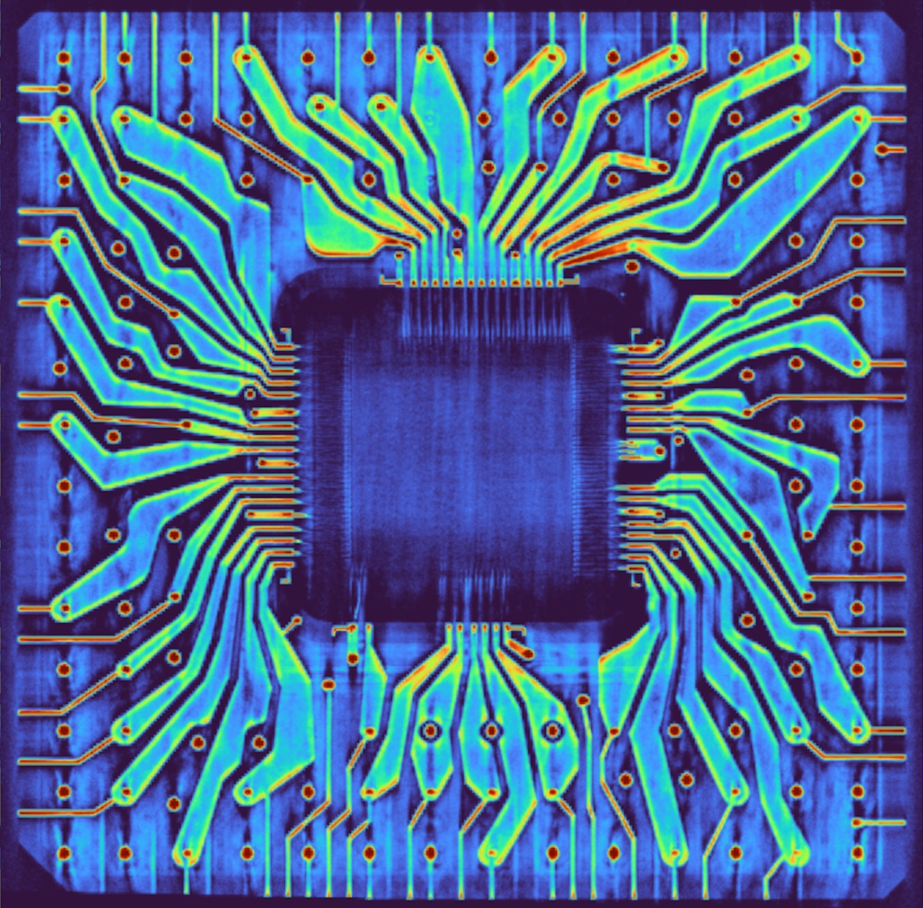
If you select the logic Vcc plane above, you'll see a bright blotchy square in the center. This is not the die itself, I think, but the adhesive that attaches the die to the package, epoxy filled with silver to provide thermal and electrical conductivity. Since silver blocks X-rays, it is highly visible in the image.
Side contacts for electroplating
What surprised me most about the scans was seeing wires that stick out to the sides of the package. These wires are used during manufacturing when the pins are electroplated with gold.5 In order to electroplate the pins, each pin must be connected to a negative voltage so it can function as a cathode. This is accomplished by giving each pin a separate wire that goes to the edge of the package.
This diagram below compares the CT scan (above) to a visual side view of the package (below). The wires are almost invisible, but can be seen as darker spots. The arrows show how three of these spots match with the CT scan; you can match up the other spots.6

Two power networks
According to the datasheet, the 386 has 20 pins connected to +5V power (Vcc) and 21 pins connected to ground (Vss). Studying the die, I noticed that the I/O circuitry in the 386 has separate power and ground connections from the logic circuitry. The motivation is that the output pins require high-current driver circuits. When a pin switches from 0 to 1 or vice versa, this can cause a spike on the power and ground wiring. If this spike is too large, it can interfere with the processor's logic, causing malfunctions. The solution is to use separate power wiring inside the chip for the I/O circuitry and for the logic circuitry, connected to separate pins. On the motherboard, these pins are all connected to the same power and ground, but decoupling capacitors absorb the I/O spikes before they can flow into the chip's logic.
The diagram below shows how the two power and ground networks look on the die, with separate pads and wiring. The square bond pads are at the top, with dark bond wires attached. The white lines are the two layers of metal wiring, and the darker regions are circuitry. Each I/O pin has a driver circuit below it, consisting of relatively large transistors to pull the pin high or low. This circuitry is powered by the horizontal lines for I/O Vcc (light red) and I/O ground (Vss, light blue). Underneath each I/O driver is a small logic circuit, powered by thinner Vcc (dark red) and Vss (dark blue). Thicker Vss and Vcc wiring goes to the logic in the rest of the chip. Thus, if the I/O circuitry causes power fluctuations, the logic circuit remains undisturbed, protected by its separate power wiring.

The datasheet doesn't mention the separate I/O and logic power networks, but by using the CT scans, I determined which pins power I/O, and which pins power logic. In the diagram below, the light red and blue pins are power and ground for I/O, while the dark red and blue pins are power and ground for logic. The pins are scattered across the package, allowing power to be supplied to all four sides of the die.

"No Connect" pins
As the diagram above shows, the 386 has eight pins labeled "NC" (No Connect)—when the chip is installed in a computer, the motherboard must leave these pins unconnected. You might think that the 132-pin package simply has eight extra, unneeded pins, but it's more complicated than that. The photo below shows five bond pads at the bottom of the 386 die. Three of these pads have bond wires attached, but two have no bond wires: these correspond to No Connect pins. Note the black marks in the middle of the pads: the marks are from test probes that were applied to the die during testing.7 The No Connect pads presumably have a function during this testing process, providing access to an important internal signal.

Seven of the eight No Connect pads are almost connected: the package has a spot for a bond wire in the die cavity and the package has internal wiring to a No Connect pin. The only thing missing is the bond wire between the pad and the die cavity. Thus, by adding bond wires, Intel could easily create special chips with these pins connected, perhaps for debugging the test process itself.
The surprising thing is that one of the No Connect pads does have the bond wire in place, completing the connection to the external pin. (I marked this pin in green in the pinout diagram earlier.) From the circuitry on the die, this pin appears to be an output. If someone with a 386 chip hooks this pin to an oscilloscope, maybe they will see something interesting.
Labeling the pads on the die
The earlier 8086 processor, for example, is packaged in a DIP (Dual-Inline Package) with two rows of pins. This makes it straightforward to figure out which pin (and thus which function) is connected to each pad on the die. However, since the 386 has a two-dimensional grid of pins, the mapping to the pads is unclear. You can guess that pins are connected to a nearby pad, but ambiguity remains. Without knowing the function of each pad, I have a harder time reverse-engineering the die.
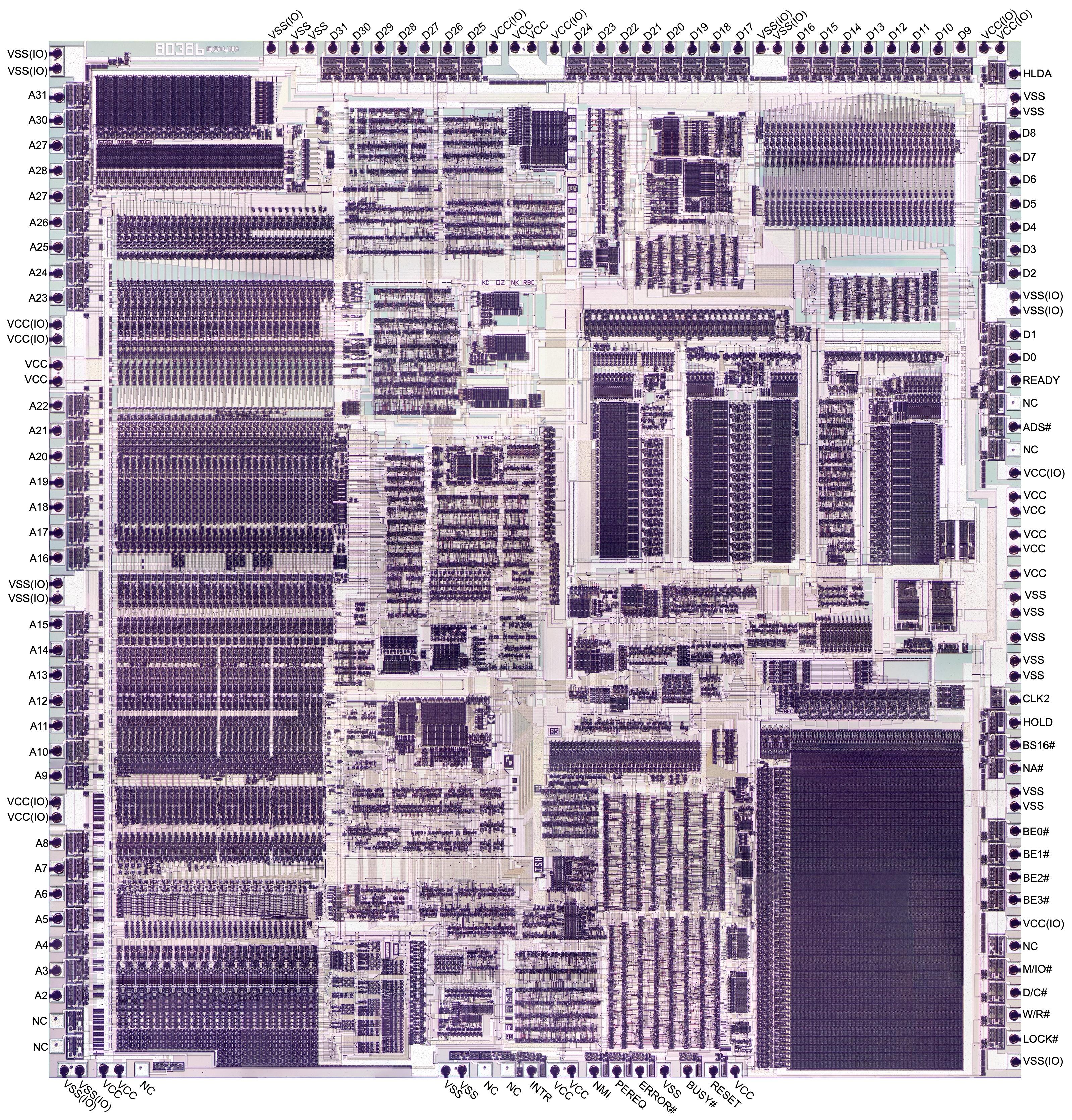
In fact, my primary motivation for scanning the 386 package was to determine the pin-to-pad mapping and thus the function of each pad.8 Once I had the CT data, I was able to trace out each hidden connection between the pad and the external pin. The image below shows some of the labels; click here for the full, completely labeled image. As far as I know, this information hasn't been available outside Intel until now.

Conclusions
Intel's early processors were hampered by inferior packages, but by the time of the 386, Intel had realized the importance of packaging. In Intel's early days, management held the bizarre belief that chips should never have more than 16 pins, even though other companies used 40-pin packages. Thus, Intel's first microprocessor, the 4004 (1971), was crammed into a 16-pin package, limiting its performance. By 1972, larger memory chips forced Intel to move to 18-pin packages, extremely reluctantly.9 The eight-bit 8008 processor (1972) took advantage of this slightly larger package, but performance still suffered because signals were forced to share pins. Finally, Intel moved to the standard 40-pin package for the 8080 processor (1974), contributing to the chip's success. In the 1980s, pin-grid arrays became popular in the industry as chips required more and more pins. Intel used a ceramic pin grid array (PGA) with 68 pins for the 186 and 286 processors (1982), followed by the 132-pin package for the 386 (1985).
The main drawback of the ceramic package was its cost. According to the 386 oral history, the cost of the 386 die decreased over time to the point where the chip's package cost as much as the die. To counteract this, Intel introduced a low-cost plastic package for the 386 that cost just a dollar to manufacture, the Plastic Quad Flat Package (PQFP) (details).
In later Intel processors, the number of connections exponentially increased. A typical modern laptop processor uses a Ball Grid Array with 2049 solder balls; the chip is soldered directly onto the circuit board. Other Intel processors use a Land Grid Array (LGA): the chip has flat contacts called lands, while the socket has the pins. Some Xeon processors have 7529 contacts, a remarkable growth from the 16 pins of the Intel 4004.
From the outside, the 386's package looks like a plain chunk of ceramic. But the CT scan revealed surprising complexity inside, from numerous contacts for electroplating to six layers of wiring. Perhaps even more secrets lurk in the packages of modern processors.
Follow me on Bluesky (@righto.com), Mastodon (@[email protected]), or RSS. (I've given up on Twitter.) Thanks to Jon Bruner and Lumafield for scanning the chip. Lumafield's interactive CT scan of the 386 package is available here if you to want to examine it yourself. Lumafield also scanned a 1960s cordwood flip-flop and the Soviet Globus spacecraft navigation instrument for us. Thanks to John McMaster for taking 2D X-rays.
Notes and references
-
I removed the metal lid with a chisel, as hot air failed to desolder the lid. A few pins were bent in the process, but I straightened them out, more or less. ↩
-
The 386 package is described in "High Performance Technology, Circuits and Packaging for the 80386", Proceedings, ICCD Conference, Oct. 1986. (Also see Design and Test of the 80386 by Pat Gelsinger, former Intel CEO.)
The paper gives the following requirements for the 386 package:
- Large pin count to handle separate 32-bit data and address buses.
- Thermal characteristics resulting in junction temperatures under 110°.
- Power supply to the chip and I/O able to supply 600mA/ns with noise levels less than 0.4V (chip) and less than 0.8V (I/O).
The first and second criteria motivated the selection of a 132-pin ceramic pin grid array (PGA). The custom six-layer package was designed to achieve the third objective. The power network is claimed to have an inductance of 4.5 nH per power pad on the device, compared to 12-14 nH for a standard package, about a factor of 3 better.
The paper states that logic Vcc, logic Vss, I/O Vcc, and I/O Vss each have 10 pins assigned. Curiously, the datasheet states that the 386 has 20 Vcc pins and 21 Vss pins, which doesn't add up. From my investigation, the "extra" pin is assigned to logic Vss, which has 11 pins. ↩
-
I estimate that the 386 package contains roughly 0.16 grams of gold, currently worth about $16. It's hard to find out how much gold is in a processor since online numbers are all over the place. Many people recover the gold from chips, but the amount of gold one can recover depends on the process used. Moreover, people tend to keep accurate numbers to themselves so they can profit. But I made some estimates after searching around a bit. One person reports 9.69g of gold per kilogram of chips, and other sources seem roughly consistent. A ceramic 386 reportedly weighs 16g. This works out to 160 mg of gold per 386. ↩
-
I don't have information on Intel's package manufacturing process specifically. This description is based on other descriptions of ceramic packages, so I don't guarantee that the details are correct for the 386. A Fujitsu patent, Package for enclosing semiconductor elements, describes in detail how ceramic packages for LSI chips are manufactured. IBM's process for ceramic multi-chip modules is described in Multi-Layer Ceramics Manufacturing, but it is probably less similar. ↩
-
An IBM patent, Method for shorting pin grid array pins for plating, describes the prior art of electroplating pins with nickel and/or gold. In particular, it describes using leads to connect all input/output pins to a common bus at the edge of the package, leaving the long leads in the structure. This is exactly what I see in the 386 chip. The patent mentions that a drawback of this approach is that the leads can act as antennas and produce signal cross-talk. Fujitsu patent Package for enclosing semiconductor elements also describes wires that are exposed at side surfaces. This patent covers methods to avoid static electricity damage through these wires. (Picking up a 386 by the sides seems safe, but I guess there is a risk of static damage.)
Note that each input/output pin requires a separate wire to the edge. However, the multiple pins for each power or ground plane are connected inside the package, so they do not require individual edge connections; one or two suffice. ↩
-
To verify that the wires from pins to the edges of the chip exist and are exposed, I used a multimeter and found connectivity between pins and tiny spots on the sides of the chip. ↩
-
To reduce costs, each die is tested while it is still part of the silicon wafer and each faulty die is marked with an ink spot. The wafer is "diced", cutting it apart into individual dies, and only the functional, unmarked dies are packaged, avoiding the cost of packaging a faulty die. Additional testing takes place after packaging, of course. ↩
-
I tried several approaches to determine the mapping between pads and pins before using the CT scan. I tried to beep out the connections between the pins and the pads with a multimeter, but because the pads are so tiny, the process was difficult, error-prone, and caused damage to the package.
I also looked at the pinout of the 386 in a plastic package (datasheet). Since the plastic package has the pins in a single ring around the border, the mapping to the die is straightforward. Unfortunately, the 386 die was slightly redesigned at this time, so some pads were moved around and new pins were added, such as
FLT#. It turns out that the pinout for the plastic chip almost matches the die I examined, but not quite. ↩ -
In his oral history, Federico Faggin, a designer of the 4004, 8008, and Z80 processors, describes Intel's fixation on 16-pin packages. When a memory chip required 18 pins instead of 16, it was "like the sky had dropped from heaven. I never seen so [many] long faces at Intel, over this issue, because it was a religion in Intel; everything had to be 16 pins, in those days. It was a completely silly requirements [sic] to have 16 pins." At the time, other manufacturers were using 40- and 48-pin packages, so there was no technical limitation, just a minor cost saving from the smaller package. ↩
10 comments:
Thank you Ken, 45 years in electronics before retirement, and your article made me realise I didn't know how ceramic packages were made!
excellent doc! thanks
Why are these so beautiful!
I don't know anything about electronics... I'm just a devops/sysadmin guy. But I love reading stuff like this, it's fascinating even though I don't understand a lot of it.
Great job! Was a pleasure to read. Thanks!
One slight thing
in this section "light red and blue pins are power and ground for I/O, while the dark red and blue pins are power and ground for logic"
blue is mentioned twice, from looking a the scan I think I/O should instead be light blue
Thank you so much! Never did I imagine I’d get to see CT scans of such a beloved chip. Thank you sir.
Normally for these packages I used micropositioner and a needle probe. Several vendors sell these and the generally just stick with at magnet to a probe station. https://everbeingprober.com/products/micropositioners-probe-holder/
Thank you for the interesting information and your work in writing this article.
I believe the 286 had 5 or 6 pads which were only bonded in special versions of the cpu, used in ICE (in circuit emulator) equipment. They provided extra information on the internal state for the emulator. Maybe the unconnected pads of the 386 are for similar purpose.
Post a Comment