I've been reverse-engineering the Intel 386 processor (from 1985), and I've come across some interesting circuits for the chip's input/output (I/O) pins. Since these pins communicate with the outside world, they face special dangers: static electricity and latchup can destroy the chip, while metastability can cause serious malfunctions. These I/O circuits are completely different from the logic circuits in the 386, and I've come across a previously-undescribed flip-flop circuit, so I'm venturing into uncharted territory. In this article, I take a close look at how the I/O circuitry protects the 386 from the "dragons" that can destroy it.
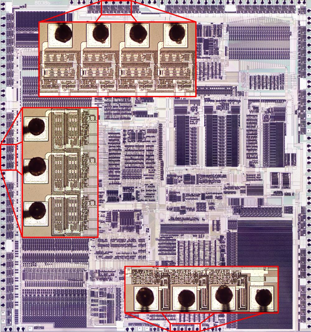
The photo above shows the die of the 386 under a microscope. The dark, complex patterns arranged in rectangular regions arise from the two layers of metal that connect the circuits on the 386 chip. Not visible are the transistors, formed from silicon and polysilicon and hidden beneath the metal. Around the perimeter of this fingernail-sized silicon die, 141 square bond pads provide the connections between the chip and the outside world; tiny gold bond wires connect the bond pads to the package. Next to each I/O pad, specialized circuitry provides the electrical interface between the chip and the external components while protecting the chip. I've zoomed in on three groups of these bond pads along with the associated I/O circuits. The circuits at the top (for data pins) and the left (for address pins) are completely different from the control pin circuits at the bottom, showing how the circuitry varies with the pin's function.
Static electricity
The first dragon that threatens the 386 is static electricity, able to burn a hole in the chip. MOS transistors are constructed with a thin insulating oxide layer underneath the transistor's gate. In the 386, this fragile, glass-like oxide layer is just 250 nm thick, the thickness of a virus. Static electricity, even a small amount, can blow a hole through this oxide layer and destroy the chip. If you've ever walked across a carpet and felt a spark when you touch a doorknob, you've generated at least 3000 volts of chip-destroying static electricity. Intel recommends an anti-static mat and a grounding wrist strap when installing a processor to avoid the danger of static electricity, also known as Electrostatic Discharge or ESD.1
To reduce the risk of ESD damage, chips have protection diodes and other components in their I/O circuitry. The schematic below shows the circuit for a typical 386 input. The goal is to prevent static discharge from reaching the inverter, where it could destroy the inverter's transistors. The diodes next to the pad provide the first layer of protection; they redirect excess voltage to the +5 rail or ground. Next, the resistor reduces the current that can reach the inverter. The third diode provides a final layer of protection. (One unusual feature of this input—unrelated to ESD—is that the input has a pull-up, which is implemented with a transistor that acts like a 20kΩ resistor.2)
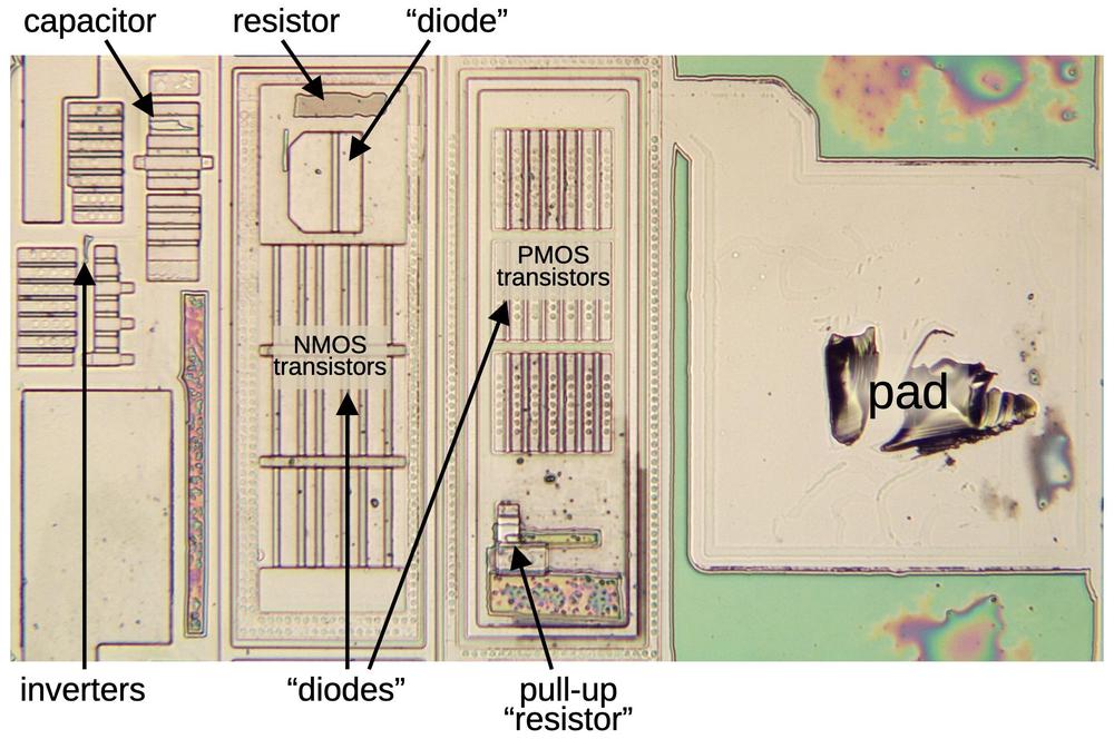
BS16# pad circuit. The BS16# signal indicates to the 386 if the external bus is 16 bits or 32 bits.The image below shows how this circuit appears on the die. For this photo, I dissolved the metal layers with acids, stripping the die down to the silicon to make the transistors visible. The diodes and pull-up resistor are implemented with transistors.3 Large grids of transistors form the pad-side diodes, while the third diode is above. The current-limiting protection resistor is implemented with polysilicon, which provides higher resistance than metal wiring. The capacitor is implemented with a plate of polysilicon over silicon, separated by a thin oxide layer. As you can see, the protection circuitry occupies much more area than the inverters that process the signal.
Latchup
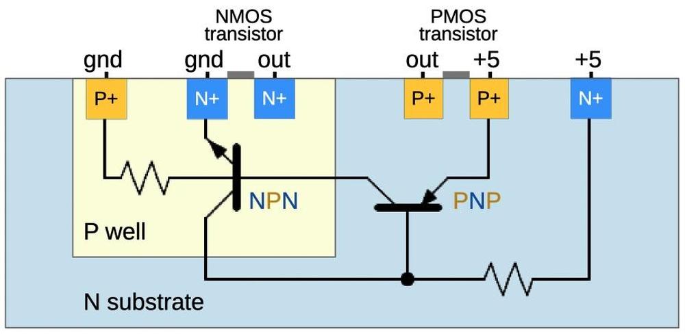
The transistors in the 386 are created by doping silicon with impurities to change its properties, creating regions of "N-type" and "P-type" silicon. The 386 chip, like most processors, is built from CMOS technology, so it uses two types of transistors: NMOS and PMOS. The 386 starts from a wafer of N-type silicon and PMOS transistors are formed by doping tiny regions to form P-type silicon embedded in the underlying N-type silicon. NMOS transistors are the opposite, with N-type silicon embedded in P-type silicon. To hold the NMOS transistors, "wells" of P-type silicon are formed, as shown in the cross-section diagram below. Thus, the 386 chip contains complex patterns of P-type and N-type silicon that form its 285,000 transistors.
But something dangerous lurks below the surface, the fire-breathing dragon of latchup waiting to burn up the chip. The problem is that these regions of N-type and P-type silicon form unwanted, "parasitic" transistors underneath the desired transistors. In normal circumstances, these parasitic NPN and PNP transistors are inactive and can be ignored. But if a current flows beneath the surface, through the silicon substrate, it can turn on a parasitic transistor and awaken the dreaded latchup.4 The parasitic transistors form a feedback loop, so if one transistor starts to turn on, it turns on the other transistor, and so forth, until both transistors are fully on, a state called latchup.5 Moreover, the feedback loop will maintain latchup until the chip's power is removed.6 During latchup, the chip's power and ground are shorted through the parasitic transistors, causing high current flow that can destroy the chip by overheating it or even melting bond wires.
Latchup can be triggered in many ways, from power supply overvoltage to radiation, but a chip's I/O pins are the primary risk because signals from the outside world are unpredictable. For instance, suppose a floppy drive is connected to the 386 and the drive sends a signal with a voltage higher than the 386's 5-volt supply. (This could happen due to a voltage surge in the drive, reflection in a signal line, or even connecting a cable.) Current will flow through the 386's protection diodes, the diodes that were described in the previous section.7 If this current flows through the chip's silicon substrate, it can trigger latchup and destroy the processor.
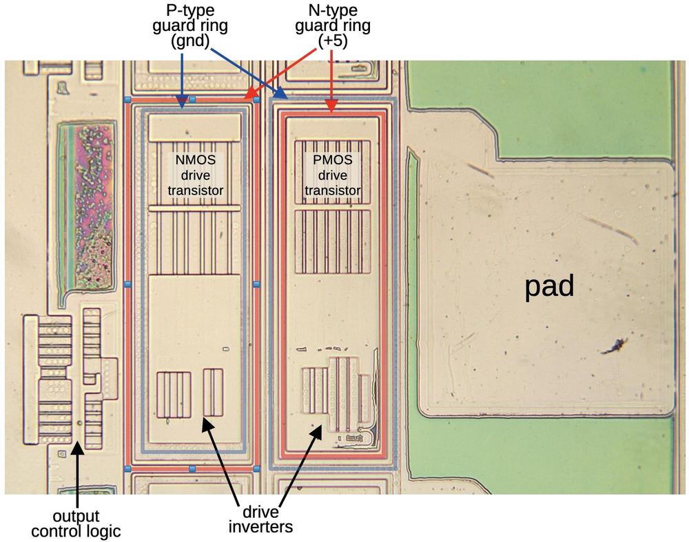
Because of this danger, the 386's I/O pads are designed to prevent latchup. One solution is to block the unwanted currents through the substrate, essentially putting fences around the transistors to keep malicious currents from escaping into the substrate. In the 386, this fence consists of "guard rings" around the I/O transistors and diodes. These rings prevent latchup by blocking unwanted current flow and safely redirecting it to power or ground.
The diagram above shows the double guard rings for a typical I/O pad.8 Separate guard rings protect the NMOS transistors and the PMOS transistors. The NMOS transistors have an inner guard ring of P-type silicon connected to ground (blue) and an outer guard ring of N-type silicon connected to +5 (red). The rings are reversed for the PMOS transistors. The guard rings take up significant space on the die, but this space isn't wasted since the rings protect the chip from latchup.
Metastability
The final dragon is metastability: it (probably) won't destroy the chip, but it can cause serious malfunctions.9 Metastability is a peculiar problem where a digital signal can take an unbounded amount of time to settle into a zero or a one. In other words, the circuit temporarily refuses to act digitally and shows its underlying analog nature.10 Metastability was controversial in the 1960s and the 1970s, with many electrical engineers not believing it existed or considering it irrelevant. Nowadays, metastability is well understood, with special circuits to prevent it, but metastability can never be completely eliminated.
In a processor, everything is synchronized to its clock. While a modern processor has a clock speed of several gigahertz, the 386's clock ran at 12 to 33 megahertz. Inside the processor, signals are carefully organized to change according to the clock—that's why your computer runs faster with a higher clock speed. The problem is that external signals may be independent of the CPU's clock. For instance, a disk drive could send an interrupt to the computer when data is ready, which depends on the timing of the spinning disk. If this interrupt arrives at just the wrong time, it can trigger metastability.
In more detail, processors use flip-flops to hold signals under the control of the clock. An "edge-triggered" flip-flop grabs its input at the moment the clock goes high (the "rising edge") and holds this value until the next clock cycle. Everything is fine if the value is stable when the clock changes: if the input signal switches from low to high before the clock edge, the flip-flop will hold this high value. And if the input signal switches from low to high after the clock edge, the flip-flop will hold the low value, since the input was low at the clock edge. But what happens if the input changes from low to high at the exact time that the clock switches? Usually, the flip-flop will pick either low or high. But very rarely, maybe a few times out of a billion, the flip-flop will hesitate in between, neither low nor high. The flip-flop may take a few nanoseconds before it "decides" on a low or high value, and the value will be intermediate until then.
The photo above illustrates a metastable signal, spending an unpredictable time between zero and one before settling on a value. The situation is similar to a ball balanced on top of a hill, a point of unstable equilibrium.11 The smallest perturbation will knock the ball down one of the two stable positions at the bottom of the hill, but you don't know which way it will go or how long it will take.
Metastability is serious because if a digital signal has a value that is neither 0 nor 1 then downstream circuitry may get confused. For instance, if part of the processor thinks that it received an interrupt and other parts of the processor think that no interrupt happened, chaos will reign as the processor takes contradictory actions. Moreover, waiting a few nanoseconds isn't a cure because the duration of metastability can be arbitrarily long. Waiting helps, since the chance of metastability decreases exponentially with time, but there is no guarantee.12
The obvious solution is to never change an input exactly when the clock changes. The processor is designed so that internal signals are stable when the clock changes, avoiding metastability. Specifically, the designer of a flip-flop specifies the setup time—how long the signal must be stable before the clock edge—and the hold time—how long the signal must be stable after the clock edge. As long as the input satisfies these conditions, typically a few picoseconds long, the flip-flop will function without metastability.
Unfortunately, the setup and hold times can't be guaranteed when the processor receives an external signal that isn't synchronized to its clock, known as an asynchronous signal. For instance, a processor receives interrupt signals when an I/O device has data, but the timing is unpredictable because it depends on mechanical factors such as a keypress or a spinning floppy disk. Most of the time, everything will work fine, but what about the one-in-a-billion case where the timing of the signal is unlucky? (Since modern processors run at multi-gigahertz, one-in-a-billion events are not rare; they can happen multiple times per second.)
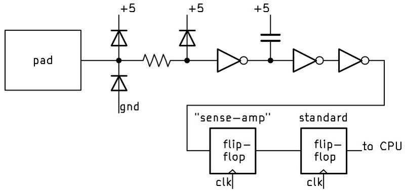
One solution is a circuit called a synchronizer that takes an asynchronous signal and synchronizes it to the clock. A synchronizer can be implemented with two flip-flops in series: even if the first flip-flop has a metastable output, chances are that it will resolve to 0 or 1 before the second flip-flop stores the value. Each flip-flop provides an exponential reduction in the chance of metastability, so using two flip-flops drastically reduces the risk. In other words, the circuit will still fail occasionally, but if the mean time between failures (MTBF) is long enough (say, decades instead of seconds), then the risk is acceptable.
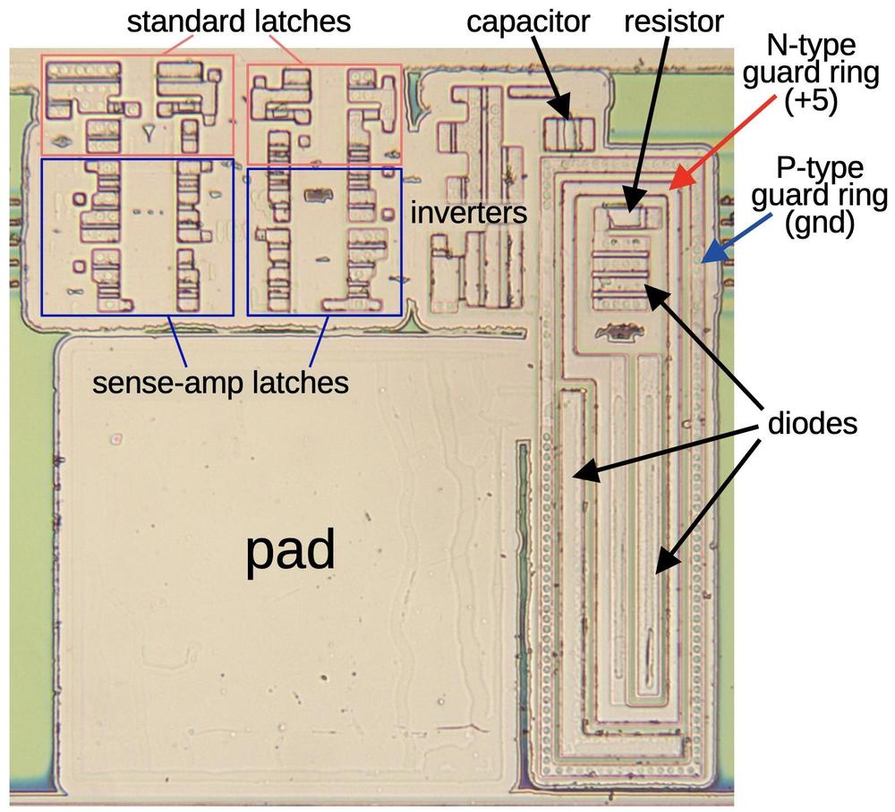
The schematic above shows how the 386 uses two flip-flops to minimize metastability. The first flip-flop is a special flip-flop that is based on a sense amplifier. It is much more complicated than a regular flip-flop, but it responds faster, reducing the chance of metastability. It is built from two of the sense-amplifier latches below, which I haven't seen described anywhere. In a DRAM memory chip, a sense amplifier takes a weak signal from a memory cell and rapidly amplifies it into a solid 0 or 1. In this flip-flop, the sense amplifier takes a potentially ambiguous signal and rapidly amplifies it into a 0 or 1. By amplifying the signal quickly, the flip-flop reduces metastability. (See the footnote for details.14)
The die photo below shows how this circuitry looks on the die. Each flip-flop is built from two latches; note that the sense-amp latches are larger than the standard latches. As before, the pad has protection diodes inside guard rings. For some reason, however, these diodes have a different structure from the transistor-based diodes described earlier. The 386 has five inputs that use this circuitry to protect against metastability.13 These inputs are all located together at the bottom of the die—it probably makes the layout more compact when neighboring pad circuits are all the same size.
In summary, the 386's I/O circuits are interesting because they are completely different from the chip's regular logic circuitry. In these circuits, the border between digital and analog breaks down; these circuits handle binary signals, but analog issues dominate the design. Moreover, hidden parasitic transistors play key roles; what you don't see can be more important than what you see. These circuits defend against three dangerous "dragons": static electricity, latchup, and metastability. Intel succeeded in warding off these dragons and the 386 was a success.
For more on the 386 and other chips, follow me on Mastodon (@[email protected]), Bluesky (@righto.com), or RSS. (I've given up on Twitter.) If you want to read more about 386 input circuits, I wrote about the clock pin here
Notes and references
-
Anti-static precautions are specified in Intel's processor installation instructions. Also see Intel's Electrostatic Discharge and Electrical Overstress Guide. I couldn't find ESD ratings for the 386, but a modern Intel chip is tested to withstand 500 volts or 2000 volts, depending on the test procedure. ↩
-
The BS16# pin is slightly unusual because it has an internal pull-up resistor. If you look at the datasheet (9.2.3 and Table 9-3 footnotes), a few input pins (ERROR#, BUSY#, and BS16#) have internal pull-up resistors of 20 kΩ, while the PEREQ input pin has an internal pull-down resistor of 20 kΩ. ↩
-
The protection diode is probably a grounded-gate NMOS (ggNMOS), an NMOS transistor with the gate, source, and body (but not the drain) tied to ground. This forms a parasitic NPN transistor under the MOSFET that dissipates the ESD. (I think that the PMOS protection is the same, except the gate is pulled high, not grounded.) For output pins, the output driver MOSFETs have parasitic transistors that make the output driver "self-protected". One consequence is that the input pads and the output pads look similar (both have large MOS transistors), unlike other chips where the presence of large transistors indicates an output. (Even so, 386 outputs and inputs can be distinguished because outputs have large inverters inside the guard rings to drive the MOSFETs, while inputs do not.) Also see Practical ESD Protection Design. ↩
-
The 386 uses P-wells in an N-doped substrate. The substrate is heavily doped with antimony, with a lightly doped N epitaxial layer on top. This doping helped provide immunity to latchup. (See "High performance technology, circuits and packaging for the 80386", ICCD 1986.) For the most part, modern chips use the opposite: N-wells with a P-doped substrate. Why the substrate change?
In the earlier days of CMOS, P-well was standard due to the available doping technology, see N-well and P-well performance comparison. During the 1980s, there was controversy over which was better: P-well or N-well: "It is commonly agreed that P-well technology has a proven reliability record, reduced alpha-particle sensitivity, closer matched p- and n- channel devices, and high gain NPN structures. N-well proponents acknowledge better compatibility and performance with NMOS processing and designs, good substrate quality, availability, and cost, lower junction capacitance, and reduced body effects." (See Design of a CMOS Standard Cell Library.)
As wafer sizes increased in the 1990s, technology shifted to P-doped substrates because it is difficult to make large N-doped wafers due to the characteristics of the dopants (link). Some chips optimize transistor characteristics by using both types of wells, called a twin-well process. For instance, the Pentium used P-doped wafers and implanted both N and P wells. (See Intel's 0.25 micron, 2.0 volts logic process technology.) ↩
-
You can also view the parasitic transistors as forming an SCR (Silicon Controlled Rectifier), a four-layer semiconductor device. SCRs were popular in the 1970s because they could handle higher currents and voltages than transistors. But as high-power transistors were developed, SCRs fell out of favor. In particular, once an SCR is turned on, it stays on until power is removed or reversed; this makes SCRs harder to use than transistors. (This is the same characteristic that makes latchup so dangerous.) ↩
-
Satellites and nuclear missiles have a high risk of latchup due to radiation. Since radiation-induced latchup cannot always be prevented, one technique for dealing with latchup is to detect the excessive current from latchup and then power-cycle the chip. For instance, you can buy a radiation-hardened current limiter chip that will detect excessive current due to latchup and temporarily remove power; this chip sells for the remarkable price of $1780.
For more on latchup, see the Texas Instruments Latch-Up white paper, as well as Latch-Up, ESD, and Other Phenomena. ↩
-
The 80386 Hardware Reference Manual discusses how a computer designer can prevent latchup in the 386. The designer is assured that Intel's "CHMOS III" process prevents latchup under normal operating conditions. However, exceeding the voltage limits on I/O pins can cause current surges and latchup. Intel provides three guidelines: observe the maximum ratings for input voltages, never apply power to a 386 pin before the chip is powered up, and terminate I/O signals properly to avoid overshoot and undershoot. ↩
-
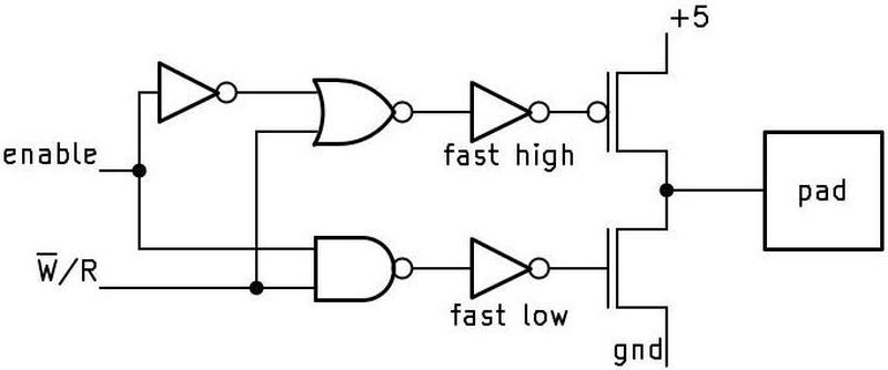
The circuit for the WR# pin is similar to many other output pins. The basic idea is that a large PMOS transistor pulls the output high, while a large NMOS transistor pulls the output low. If the
enableinput is low, both transistors are turned off and the output floats. (This allows other devices to take over the bus in the HOLD state.)Schematic for the WR# pin driver.The inverters that control the drive transistors have an unusual layout. These inverters are inside the guard rings, meaning that the inverters are split apart, with the NMOS transistors in one ring and PMOS transistors in the other. The extra wiring adds capacitance to the output which probably makes the inverters slightly slower.
These inverters have a special design: one inverter is faster to go high than to go low, while the other inverter is the opposite. The motivation is that if both drive transistors are on at the same time, a large current will flow through the transistors from power to ground, producing an unwanted current spike (and potentially latchup). To avoid this, the inverters are designed to turn one drive transistor off faster than turning the other one on. Specifically, the high-side inverter has an extra transistor to quickly pull its output high, while the low-side inverter has an extra transistor to pull the output low. Moreover, the inverter's extra transistor is connected directly to the drive transistors, while the inverter's main output connects through a longer polysilicon path with more resistance, providing an RC delay. I found this layout very puzzling until I realized that the designers were carefully controlling the turn-on and turn-off speeds of these inverters. ↩
-
In Metastability and Synchronizers: A Tutorial, there's a story of a spacecraft power supply being destroyed by metastability. Supposedly, metastability caused the logic to turn on too many units, overloading and destroying the power supply. I suspect that this is a fictional cautionary tale, rather than an actual incident.
For more on metastability, see this presentation and this writeup by Tom Chaney, one of the early investigators of metastability. ↩
-
One of Vonada's Engineering Maxims is "Digital circuits are made from analog parts." Another maxim is "Synchronizing circuits may take forever to make a decision." These maxims and a dozen others are from Don Vonada in DEC's 1978 book Computer Engineering. ↩
-
Curiously, the definition of metastability in electronics doesn't match the definition in physics and chemistry. In electronics, a metastable state is an unstable equilibrium. In physics and chemistry, however, a metastable state is a stable state, just not the most stable ground state, so a moderate perturbation will knock it from the metastable state to the ground state. (In the hill analogy, it's as if the ball is caught in a small basin partway down the hill.) ↩
-
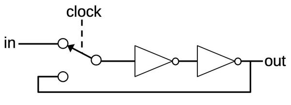
In case you're wondering what's going on with metastability at the circuit level, I'll give a brief explanation. A typical flip-flop is based on a latch circuit like the one below, which consists of two inverters and an electronic switch controlled by the clock. When the clock goes high, the inverters are configured into a loop, latching the prior input value. If the input was high, the output from the first inverter is low and the output from the second inverter is high. The loop feeds this output back into the first inverter, so the circuit is stable. Likewise, the circuit can be stable with a low input.
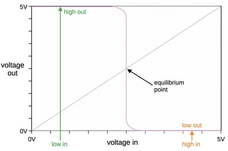
A latch circuit.But what happens if the clock flips the switch as the input is changing, so the input to the first inverter is somewhere between zero and one? We need to consider that an inverter is really an analog device, not a binary device. You can describe it by a "voltage transfer curve" (purple line) that specifies the output voltage for a particular input voltage. For example, if you put in a low input, you get a high output, and vice versa. But there is an equilibrium point where the output voltage is the same as the input voltage. This is where metastability happens.
The voltage transfer curve for a hypothetical inverter.Suppose the input voltage to the inverter is the equilibrium voltage. It's not going to be precisely the equilibrium voltage (because of noise if nothing else), so suppose, for example, that it is 1µV above equilibrium. Note that the transfer curve is very steep around equilibrium, say a slope of 100, so it will greatly amplify the signal away from equilibrium. Thus, if the input is 1µV above equilibrium, the output will be 100µV below equilibrium. Then the next inverter will amplify again, sending a signal 10mV above equilibrium back to the first inverter. The distance will be amplified again, now 1000mV below equilibrium. At this point, you're on the flat part of the curve, so the second inverter will output +5V and the first inverter will output 0V, and the circuit is now stable.
The point of this is that the equilibrium voltage is an unstable equilibrium, so the circuit will eventually settle into the +5V or 0V states. But it may take an arbitrary number of loops through the inverters, depending on how close the starting point was to equilibrium. (The signal is continuous, so referring to "loops" is a simplification.) Also note that the distance from equilibrium is amplified exponentially with time. This is why the chance of metastability decreases exponentially with time. ↩
-
Looking at the die shows that the pins with metastability protection are
INTR,NMI,PEREQ,ERROR#, andBUSY#. The 80386 Hardware Reference Manual lists these same five pins as asynchronous—I like it when I spot something unusual on the die and then discover that it matches an obscure statement in the documentation. The interrupt pinsINTRandNMIare asynchronous because they come from external sources that may not be using the 386's clock. But what aboutPEREQ,ERROR#, andBUSY#? These pins are part of the interface with an external math coprocessor (the 287 or 387 chip). In most cases, the coprocessor uses the 386's clock. However, the 387 supported a little-used asynchronous mode where the processor and the coprocessor could run at different speeds. ↩ -
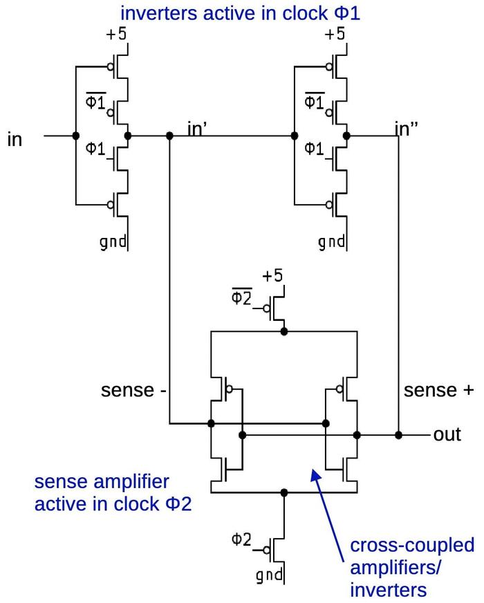
The 386's metastability flip-flop is constructed with an unusual circuit. It has two latch stages (which is normal), but instead of using two inverters in a loop, it uses a sense-amplifier circuit. The idea of the sense amplifier is that it takes a differential input. When the clock enables the sense amplifier, it drives the higher input high and the lower input low (the inputs are also the outputs). (Sense amplifiers are used in dynamic RAM chips to amplify the tiny signals from a RAM cell to form a 0 or 1. At the same time, the amplifier refreshes the DRAM cell by generating full voltages.) Note that the sense amplifier's inputs also act as outputs; inputs during clock phase 1 and outputs during phase 2.
The schematic shows one of the latch stages; the complete flip-flop has a second stage, identical except that the clock phases are switched. This latch is much more complex than the typical 386 latch; 14 transistors versus 6 or 8. The sense amplifier is similar to two inverters in a loop, except they share a limited power current and a limited ground current. As one inverter starts to go high, it "steals" the supply current from the other. Meanwhile, the other inverter "steals" the ground current. Thus, a small difference in inputs is amplified, just as in a differential amplifier. Thus, by combining the amplification of a differential amplifier with the amplification of the inverter loop, this circuit reaches its final state faster than a regular inverter loop.
In more detail, during the first clock phase, the two inverters at the top generate the inverted and non-inverted signals. (In a metastable situation, these will be close to the midpoint, not binary.) During the second clock phase, the sense amplifier is activated. You can think of it as a differential amplifier with cross-coupling. If one input is slightly higher than the other, the amplifier pulls that input higher and the input lower, amplifying the difference. (The point is to quickly make the difference large enough to resolve the metastability.)
I couldn't find any latches like this in the literature. Comparative Analysis and Study of Metastability on High-Performance Flip-Flops describes eleven high-performance flip-flops. It includes two flip-flops that are based on sense amplifiers, but their circuits are very different from the 386 circuit. Perhaps the 386 circuit is an Intel design that was never publicized. In any case, let me know if this circuit has an official name. ↩



14 comments:
Ken, I sure hope you are going to turn all of this into a book someday.
When others (non-intel) produced the licensed design, did they always implement everything the same way, as in, did they use the same masters or were they independent to the same specification?
Isn't "The pull-up resistor is implemented with polysilicon" actually referring to the resistor that isn't the pull-up?
Dr Jaymz: I think licensed designs could go either way, but I'm not sure.
Andreas: you're right; I've fixed that.
One nit to pick. You used KΩ throughout, which should be kΩ (lower k). Though the kelvin-ohm seems like an interesting unit…
Hi Ken,
I'm always excited to see a new "Righto - new message" announcement in my inbox, and this installment didn't disappoint.
I've been doing a lot of reading on early flip-flops and your "sense amp" flip-flop caught my eye. I think you may have found a D-type double edge triggered (DET) flip-flop of the type described by Gago et al:
A. Gago, R. Escano, and J. A. Hidalgo, “Reduced implementation of D-type DET flip-flops,” IEEE Journal of Solid-State Circuits, vol. 28, no. 3, pp. 400–402, Mar. 1993, doi: 10.1109/4.210012.
Here's a link to an Electrical Engineering Stack Exchange question about it that includes the diagram and a link to the academic paper that explains its operation:
https://electronics.stackexchange.com/questions/245695/dual-edge-triggered-d-flip-flip-cmos-implementation-less-than-20-transistors
I'm looking forward to your next posting.
Thanks,
Rob
Rob: thanks for finding that! It looks very much like the circuit that I found. It's interesting that the paper was 8 years after the 386 came out; I guess the authors rediscovered the circuit in the context of double edge triggered flip-flops.
StephenD: I suppose you object to 1 MH inductors, too. I'm used to the old-school upper-case units, although I draw the line at MMF (micro-micro farad) for pF. But seriously, I've updated the post to use "k" instead of "K".
Good explanation of metastability. It is psychologically interesting that it took so long for people to accept the existence of this phenomenon.
Ken, Ken!
>In Metastability and Synchronizers: A Tutorial, there's a story of a spacecraft power supply being destroyed by metastability. Supposedly, metastability caused the logic to turn on too many units, overloading and destroying the power supply. I suspect that this is a fictional cautionary tale, rather than an actual incident.
You have said enough to identify the logic, years and the satellites involved. It likely involved the MOTOROLA encapsulated logic gates you have scanned before, and the satellited had been named "spacecraft" for its maneuverability and special abilities. But ho-boy, had it been the most launched mission by far, with so many failures before they got to anything resembling a successful mission! It makes a worthy reading, if you know HOW to read between the lines and connect the dots. Because even at this day, some people involved as station operators had not connected the dots themselves, or at least you could assume that, reading what they write online. (assumed either of which is true)
Either way, find the early satellite history, you will find a movie. It's script had undergone a security review before filming and publishing, so that it is not all accurate, but good enough. It shows the FRUSTRATION the people involved had to endure... but now you had brought it up... what if the unreliability of many of the rocket types had been caused by defective logic design, that involved "undefined" and "metastable" logic states allowed by careless design?
Metastability is rare, because for it to occur, the relative timing between the data and the clock needs to hit an extremely shot duration vulnerable window. But there is a simple trick to produce metastable behavior on purpose. I think there was an app note, possibly by Jim Williams, explaining this technique.
In a nutshell, the ideas is as follows. Suppose we we have a D-type flip-flop, and the input data transitions low to high around the vulnerable interval. Then, if the transition occurs too early, one is latched in, and if the transition is too late, a zero is latched in, and when the transition occurs right in the middle, we get the metastable state.
So what we do, we low-pass filter the output signal, and feed it back into a voltage-controlled delay line for the data input. The controlled RC delay can be made by using junction capacitance of a reverse-biased diode -- the greater the voltage the lower the capacitance, the lower the delay.
Of course the circuit and the clock both have to be reasonably low-noise in order for this to work correctly, and the demonstration would be easier with the older, slower logic families.
As the rumored satellite in question was a design of the 1960's, there is no shortage of "slower logic families" of that era of 1950-1960. Between Whiskers and Metastability is a really cold, hard place where no one can hear you scream.
From the context it is obviously clear that it is not a Kelvin-Ohm, but a digital 1024-Ohm unit... duhh.
Bingo!
I've always been curious to know how they partially solved the static electricity problem that damages chips, a very common problem in previous chips.
And even better, a reverse engineering approach.
Thank you very much for the information.
Yes, when I watch retro computing channels I think many don't know and we've perhaps all forgotten how fragile some chips were. It particular bad RAM, I would imagine, is almost always hidden damage that often doesn't fail immediately leading people to say "I've never had a problem with static damage", but they would be very wrong about that.
You see people unsoldering and popping each one into a RAM tester on a table with no ESD protection and a year or two later those chips become junk. Half were junk from the manufacturing process anyway back then!
Post a Comment