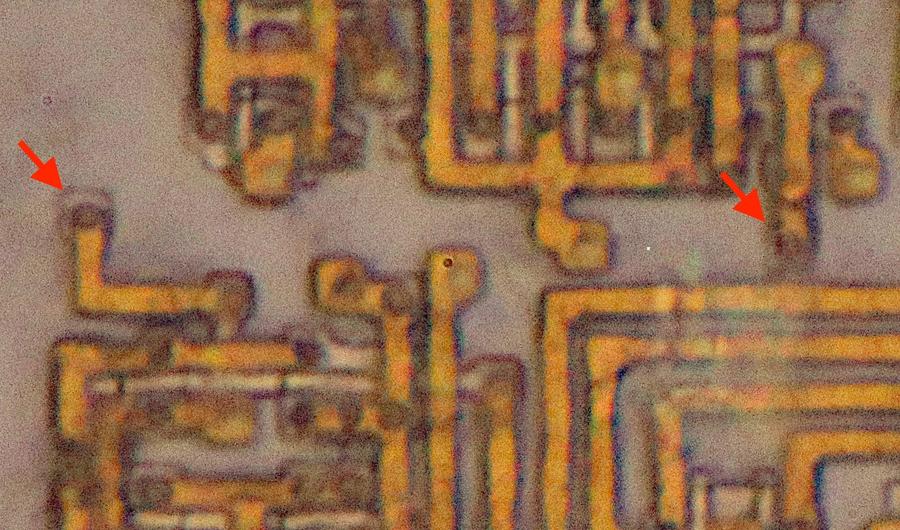
I was studying the silicon die of the Pentium processor and noticed some puzzling structures where signal lines were connected to the silicon substrate for no apparent reason. Two examples are in the photo below, where the metal wiring (orange) connects to small square regions of doped silicon (gray), isolated from the rest of the circuitry. I did some investigation and learned that these structures are "antenna diodes," special diodes that protect the circuitry from damage during manufacturing. In this blog post, I discuss the construction of the Pentium and explain how these antenna diodes work.
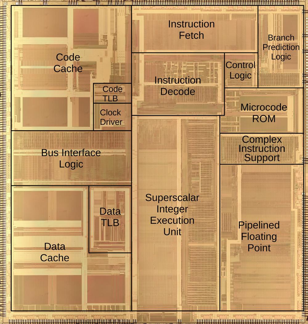
Intel released the Pentium processor in 1993, starting a long-running brand of high-performance processors: the Pentium Pro, Pentium II, and so on. In this post, I'm studying the original Pentium, which has 3.1 million transistors.1 The die photo below shows the Pentium's fingernail-sized silicon die under a microscope. The chip has three layers of metal wiring on top of the silicon so the underlying silicon is almost entirely obscured.
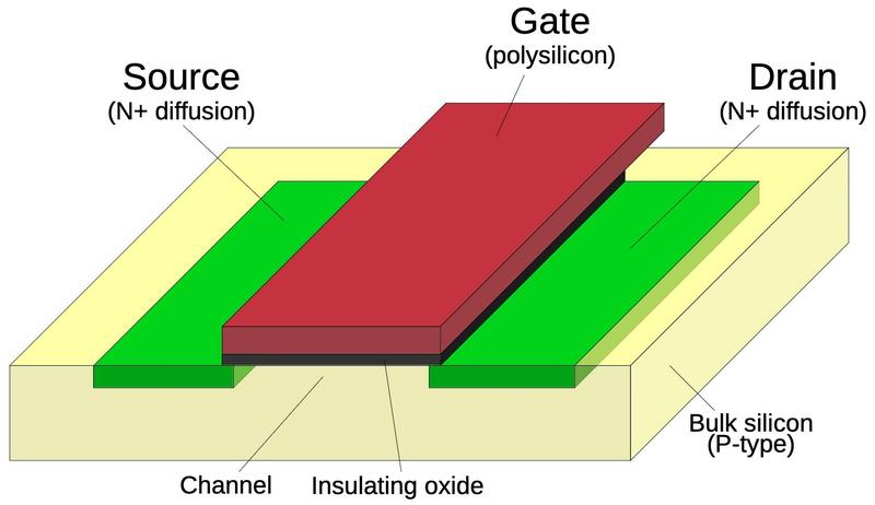
Modern processors are built from CMOS circuitry, which uses two types of transistors: NMOS and PMOS. The diagram below shows how an NMOS transistor is constructed. A transistor can be considered a switch between the source and drain, controlled by the gate. The source and drain regions (green) consist of silicon doped with impurities to change its semiconductor properties, forming N+ silicon. The gate consists of a layer of polysilicon (red), separated from the silicon by an absurdly thin insulating oxide layer. Since the oxide layer is just a few hundred atoms thick,2 it is very fragile and easily damaged by excess voltage. (This is why CMOS chips are sensitive to static electricity.) As we will see, the oxide layer can also be damaged by voltage during manufacturing.
The Pentium processor is constructed from multiple layers. Starting at the bottom, the Pentium has millions of transistors similar to the diagram above. Polysilicon wiring on top of the silicon not only forms the transistor gates but also provides short-range wiring. Above that, three layers of metal wiring connect the parts of the chip. Roughly speaking, the bottom layer of metal connects to the silicon and polysilicon to construct logic gates from the transistors, while the upper layers of wiring travel longer distances, with one layer for signals traveling horizontally and the other layer for signals traveling vertically. Tiny tungsten plugs called vias provide connections between the different layers of wiring. A key challenge of chip design is routing, directing signals through the multiple layers of wiring while packing the circuitry as densely as possible.
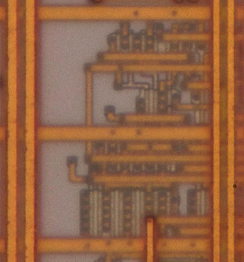
The photo below shows a small region of the Pentium die with the three metal layers visible. The golden vertical lines are the top metal layer, formed from aluminum and copper. Underneath, you can see the horizontal wiring of the middle metal layer. The more complex wiring of the bottom metal layer can be seen, along with the silicon and polysilicon that form transistors. The small black dots are the tungsten vias that connect metal layers, while the larger dark circles are contacts with the underlying silicon or polysilicon. Near the bottom of the photo, the vertical gray bands are polysilicon lines, forming transistor gates. Although the chip appears flat, it has a three-dimensional structure with multiple layers of metal separated by insulating layers of silicon dioxide. This three-dimensional structure will be important in the discussion below. (The metal wiring is much denser over most of the chip; this region is one of the rare spots where all the layers are visible.)
The manufacturing process for an integrated circuit is extraordinarily complicated but I'll skip over most of the details and focus on how each metal layer is constructed, layer by layer. First, a uniform metal layer is constructed over the silicon wafer. Next, the desired pattern is produced on the surface using a process called photolithography: a light-sensitive chemical called "resist" is applied to the wafer and exposed to light through a patterned mask. The light hardens the resist, creating a protective coating with the pattern of the desired wiring. Finally, the unprotected metal is etched away, leaving the wiring.
In the early days of integrated circuits, the metal was removed with liquid acids, a process called wet etching. Inconveniently, wet etching tended to eat away metal underneath the edges of the mask, which became a problem as integrated circuits became denser and the wires needed to be thinner. The solution was dry etch, using a plasma to remove the metal. By applying a large voltage to plates above and below the chip, a gas such as HCl is ionized into a highly reactive plasma. This plasma attacks the surface (unless it is protected by the resist), removing the unwanted metal. The advantage of dry etching is that it can act vertically (anisotropically), providing more control over the line width.
Although plasma etching improved the etching process, it caused another problem: plasma-induced oxide damage, also called (metaphorically) the "antenna effect."3 The problem is that long metal wires on the chip could pick up an electrical charge from the plasma, producing a large voltage. As described earlier, the thin oxide layer under a transistor's gate is sensitive to voltage damage. The voltage induced by the plasma can destroy the transistor by blowing a hole through the gate oxide or it can degrade the transistor's performance by embedding charges inside the oxide layer.4
Several factors affect the risk of damage from the antenna effect. First, only the transistor's gate is sensitive to the induced voltage, due to the oxide layer. If the wire is also connected to a transistor's source or drain, the wire is "safe" since the source and drain provide connections to the chip's substrate, allowing the charge to dissipate harmlessly. Note that when the chip is completed, every transistor gate is connected to another transistor's source or drain (which provides the signal to the gate), so there is no risk of damage. Thus, the problem can only occur during manufacturing, with a metal line that is connected to a gate on one end but isn't connected on the other end. Moreover, the highest layer of metal is "safe" since everything is connected at that point. Another factor is that the induced voltage is proportional to the length of the metal wire, so short wires don't pose a risk. Finally, only the metal layer currently being etched poses a risk; since the lower layers are insulated by the thick oxide between layers, they won't pick up charge.
These factors motivate several ways to prevent antenna problems.5 First, a long wire can be broken into shorter segments, connected by jumpers on a higher layer. Second, moving long wires to the top metal layer eliminates problems.6 Third, diodes can be added to drain the charge from the wire; these are called "antenna diodes". When the chip is in use, the antenna diodes are reverse-biased so they have no electrical effect. But during manufacturing, the antenna diodes let charge flow to the substrate before it causes problems.
The third solution, the antenna diodes, explains the mysterious connections that I saw in the Pentium. In the diagram below, these diodes are visible on the die as square regions of doped silicon. The larger regions of doped silicon form PMOS transistors (upper) and NMOS transistors (lower). The polysilicon lines are faintly visible; they form transistor gates where they cross the doped silicon. (For this photo, I removed all the metal wiring.)
Confusingly, the antenna diodes look almost identical to "well taps", connections from the substrate to the chip's positive voltage supply, but have a completely different purpose. In the Pentium, the PMOS transistors are constructed in "wells" of N-type silicon. These wells must be raised to the chip's positive voltage, so there are numerous well tap connections from the positive supply to the wells. The well taps consist of squares of N+ doped silicon in the the N-type silicon well, providing an electrical connection. On the other hand, the antenna diodes also consist of N+ doped silicon, but embedded in P-type silicon. This forms a P-N junction that creates the diode.
In the Pentium, antenna diodes are used for only a small fraction of the wiring. The diodes require extra area on the die, so they are used only when necessary. Most of the antenna problems on the Pentium were apparently resolved through routing. Although the antenna diodes are relatively rare, they are still frequent enough that they caught my attention.
Antenna effects are still an issue in modern integrated circuits. Integrated circuit fabricators provide rules on the maximum allowable size of antenna wires for a particular manufacturing process.7 Software checks the design to ensure that the antenna rules are not violated, modifying the routing and inserting diodes as necessary. Violating the antenna rules can result in damaged chips and a very low yield, so it's more than just a theoretical issue.
Thanks to /r/chipdesign and Discord for discussion. If you're interested in the Pentium, I've written about standard cells in the Pentium, and the Pentium as a Navajo rug. Follow me on Mastodon (@[email protected]) or Bluesky (@righto.com) or RSS for updates.
Notes and references
-
In this post, I'm looking at the Pentium model 80501 (codenamed P5). This model was soon replaced with a faster, lower-power version called the 80502 (P54C). Both are considered original Pentiums. ↩
-
IC manufacturing drives CPU performance states that gate oxide thickness was 100 to 300 angstroms in 1993. ↩
-
The wires are acting metaphorically as antennas, not literally, as they collect charge, not picking up radio waves.
Plasma-induced oxide damage gave rise to research and conferences in the 1990s to address this problem. The International Symposium on Plasma- and Process-Induced Damage started in 1996 and continued until 2003. Numerous researchers from semiconductor companies and academia studied the causes and effects of plasma damage. ↩
-
The damage is caused by "Fowler-Nordheim tunneling", where electrons tunnel through the oxide and cause damage. Flash memory uses this tunneling to erase the memory; the cumulative damage is why flash memory can only be written a limited number of times. ↩
-
Some relevant papers: Magnetron etching of polysilicon: Electrical damage (1991), Thin-oxide damage from gate charging during plasma processing (1992), Antenna protection strategy for ultra-thin gate MOSFETs (1998), Fixing antenna problem by dynamic diode dropping and jumper insertion (2000). The Pentium uses the "dynamic diode dropping" approach, adding antenna diodes only as needed, rather than putting them in every circuit. I noticed that the Pentium uses extension wires to put the diode in a more distant site if there is no room for the diode under the existing wiring. As an aside, the third paper uses the curious length unit of kµm; by calling 1000 µm a kµm, you can think in micrometers, even though this unit is normally called a mm. ↩
-
Sources say that routing signals on the top metal prevents antenna violations. However, I see several antenna diodes in the Pentium that are connected directly from the bottom metal (M1) through M2 to long lines on M3. These diodes seem redundant since the source/drain connections are in place by that time. So there are still a few mysteries... ↩
-
Foundries have antenna rules provided as part of the Process Design Kit (PDK). Here are the rules for MOSIS and SkyWater. I've focused on antenna effects from the metal wiring, but polysilicon and vias can also cause antenna damage. Thus, there are rules for these layers too. Polysilicon wiring is less likely to cause antenna problems, though, as it is usually restricted to short distances due to its higher resistance. ↩


