How Hacker News ranking really works: scoring, controversy, and penalties

The basic formula for Hacker News ranking has been known for years, but questions remained. Does the published code give the real algorithm? Are rankings purely based on votes or do invisible factors come into play? Do stories about the NSA get pushed down in the rankings? Why did that popular story suddenly disappear from the front page after you commented on it?

By carefully analyzing the top 60 HN stories for several days, I can answer those questions and more. The published formula is mostly accurate. There is much more tweaking of rankings than you'd expect, with 20% of front-page stories getting penalized in various ways. Anything with "NSA" in the title is penalized and drops off quickly. A "controversial" story gets severely penalized after hitting 40 comments. This article describes scoring and penalties in detail. [Edit: HN no longer penalizes NSA articles (details).]

How ranking works

Articles are scored based on their upvote score, the time since the article was submitted, and various penalties using the following formula: score=\frac{ \left( votes-1 \right) ^{.8}}{ \left( age _{hours} + 2 \right) ^ {1.8}} * penalties

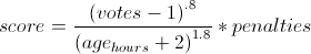
Because the time has a larger exponent than the votes, an article's score will eventually drop to zero, so nothing stays on the front page too long. This exponent is known as gravity.

You might expect that every time you visit Hacker News, the stories are scored by the above formula and sorted to determine their rankings. But for efficiency, stories are individually reranked only occasionally. When a story is upvoted, it is reranked and moved up or down the list to its appropriate spot, leaving the other stories unchanged. Thus, the amount of reranking is significantly reduced. There is, however, the possibility that a story stops getting votes and ends up stuck in a high position. To avoid this, every 30 seconds one of the top 50 stories is randomly selected and reranked. The consequence is that a story may be "wrongly" ranked for many minutes if it isn't getting votes. In addition, pages can be cached for 90 seconds.

Raw scores and the #1 spot on a typical day

The following image shows the raw scores (excluding penalties) for the top 60 HN articles throughout the day of November 11. Each line corresponds to an article, colored according to its position on the page. The red line shows the top article on HN. Note that because of penalties, the article with the top raw score often isn't the top article.

Hacker News raw article scores throughout a day. Red line indicates the #1 article. Due to penalties, the #1 article does not always have the top score.

This chart shows a few interesting things. The score for an article shoots up rapidly and then slowly drops over many hours. The scoring formula accounts for much of this: an article getting a constant rate of votes will peak quickly and then gradually descend. But the observed peak is even faster - this is because articles tend to get a lot of votes in the first hour or two, and then the voting rate drops off. Combining these two factors yields the steep curves shown.

There are a few articles each day that score much above the rest, along with a lot of articles in the middle. Some articles score very well but are unlucky and get stuck behind a more popular article. Other articles hit #1 briefly, between the fall of one and the climb of another.

Looking at the difference between the article with the top raw score (top of the graph) and the top-ranked article (red line), you can see when penalties have been applied. The article Getting website registration completely wrong hit #1 early in the morning, but was penalized for controversy and rapidly dropped down the page, letting Linux ate my RAM briefly get the #1 spot before Simpsons in CSS overtook it. A bit later, the controversy penalty was applied to Apple Maps shortly after it reached the #1 spot, causing it to lose its #1 spot and rapidly drop down the rankings. The Snapchat article reached the top of HN but was penalized so heavily at 8:22 am that it dropped off the chart entirely. Why you should never use MongoDB was hugely popular and would have spent much of the day in the #1 spot, except it was rapidly penalized and languished around #7. Severing ties with the NSA started off with a NSA penalty but was so hugely popular it still got the #1 spot. However, it was quickly given an even bigger penalty, forcing it down the page. Finally, near the end of the day $4.1m goes missing was penalized. As it turns out, it would have soon lost the #1 spot to FTL even without the penalty.

The green triangles and text show where "controversy" penalties were applied. The blue triangles and text show where articles were penalized into oblivion, dropping off the top 60. Milder penalties are not shown here.

It's clear that the content of the #1 spot on HN isn't "natural", but results from the constant application of penalties to many articles. It's unclear if these penalties result from HN administrators or from flagged articles.

Submissions that get automatically penalized

Some submissions get automatically penalized based on the title, and others get penalized based on the domain. It appears that any article with NSA in the title gets an automatic penalty of .4. I looked for other words causing automatic penalties, such as awesome, bitcoin, and bubble but they do not seem to get penalized. I observed that many websites appear to automatically get a penalty of .25 to .8: arstechnica.com, businessinsider.com, easypost.com, github.com, imgur.com, medium.com, quora.com, qz.com, reddit.com, rt.com, stackexchange.com, theguardian.com, theregister.com, theverge.com, torrentfreak.com, youtube.com. I'm sure the actual list is longer. (This is separate from "banned" sites, which were listed at one point.

One interesting theory by eterm is that news from popular sources gets submitted in parallel by multiple people resulting in more upvotes than the article "merits". Automatically penalizing popular websites would help counteract this effect.

The impact of penalties

Using the scoring formula, the impact of a penalty can be computed. If an article gets a penalty factor of .4, this is equivalent to each vote only counting as .3 votes. Alternatively, the article will drop in ranking 66% faster than normal. A penalty factor of .1 corresponds to each vote counting as .05 votes, or the article dropping at 3.6 times the normal rate. Thus, a penalty factor of .4 has a significant impact, and .1 is very severe.

Controversy In order to prevent flamewars on Hacker News, articles with "too many" comments will get heavily penalized as "controversial". In the published code, the contro-factor function kicks in for any post with more than 20 comments and more comments than upvotes. Such an article is scaled by (votes/comments)^2. However, the actual formula is different - it is active for any post with more comments than upvotes and at least 40 comments. Based on empirical data, I suspect the exponent is 3, rather than 2 but haven't proven this. The controversy penalty can have a sudden and catastrophic effect on an article's ranking, causing an article to be ranked highly one minute and vanish when it hits 40 comments. If you've wondered why a popular article suddenly vanishes from the front page, controversy is a likely cause. For example, Why the Chromebook pundits are out of touch with reality dropped from #5 to #22 the moment it hit 40 comments, and Show HN: Get your health records from any doctor' was at #17 but vanished from the top 60 entirely on hitting 40 comments.

My methodology

I crawled the /news and /news2 pages every minute (staying under the 2 pages per minute guideline). I parsed the (somewhat ugly) HTML with Beautiful Soup, processed the results with a big pile of Python scripts, and graphed results with the incomprehensible but powerful matplotlib. The basic idea behind the analysis is to generate raw scores using the formula and then look for anomalies. At a point in time (e.g. 11/09 8:46), we can compute the raw scores on the top 10 stories:

2.802 Pyret: A new programming language from the creators of Racket
1.407 The Big Data Brain Drain: Why Science is in Trouble
1.649 The NY Times endorsed a secretive trade agreement that the public can't read
0.785 S.F. programmers build alternative to HealthCare.gov (warning: autoplay video)
0.844 Marelle: logic programming for devops
0.738 Sprite Lamp
0.714 Why Teenagers Are Fleeing Facebook
0.659 NodeKnockout is in Full Tilt. Checkout some demos
0.805 ISO 1
0.483 Shopify accepts Bitcoin.
0.452 Show HN: Understand closures
Note that three of the top 10 articles are ranked lower than expected from their score: The NY Times, Marelle and ISO 1. Since The NY Times is ranked between articles with 1.407 and 0.785, its penalty factor can be computed as between .47 and .85. Likewise, the other penalties must be .87 to .93, and .60 to .82. I observed that most stories are ranked according to their score, and the exceptions are consistently ranked much lower, indicating a penalty. This indicates that the scoring formula in use matches the published code. If the formula were different, for instance the gravity exponent were larger, I'd expect to see stories drift out of their "expected" ranking as their votes or age increased, but I never saw this.

This technique shows the existence of a penalty and gives a range for the penalty, but determining the exact penalty is difficult. You can look at the range over time and hope that it converges to a single value. However, several sources of error mess this up. First, the neighboring articles may also have penalties applied, or be scored differently (e.g. job postings). Second, because articles are not constantly reranked, an article may be out of place temporarily. Third, the penalty on an article may change over time. Fourth, the reported vote count may differ from the actual vote count because "bad" votes get suppressed. The result is that I've been able to determine approximate penalties, but there is a fair bit of numerical instability.

Penalties over a day

The following graph shows the calculated penalties over the course of a day. Each line shows a particular article. It should start off at 1 (no penalty), and then drop to a penalty level when a penalty is applied. The line ends when the article drops off the top 60, which can be fairly soon after the penalty is applied. There seem to be penalties of 0.2 and 0.4, as well as a lot in the 0.8-0.9 range. It looks like a lot of penalties are applied at 9am (when moderators arrive?), with more throughout the day. I'm experimenting with different algorithms to improve the graph since it is pretty noisy.
On average, about 20% of the articles on the front page have been penalized, while 38% of the articles on the second page have been penalized. (The front page rate is lower since penalized articles are less likely to be on the front page, kind of by definition.) There is a lot more penalization going on than you might expect.

Here's a list of the articles on the front page on 11/11 that were penalized. (This excludes articles that would have been there if they weren't penalized.) This list is much longer than I expected; scroll for the full list.

Why the Climate Corporation Sold Itself to Monsanto, Facebook Publications, Bill Gates: What I Learned in the Fight Against Polio, McCain says NSA chief Keith Alexander 'should resign or be fired', You are not a software engineer, What is a y-combinator?, Typhoon Haiyan kills 10,000 in Philippines, To Persuade People, Tell Them a Story, Tetris and The Power Of CSS, Microsoft Research Publications, Moscow subway sells free tickets for 30 sit-ups, The secret world of cargo ships, These weeks in Rust, Empty-Stomach Intelligence, Getting website registration completely wrong, The Six Most Common Species Of Code, Amazon to Begin Sunday Deliveries, With Post Office's Help, Linux ate my RAM, Simpsons in CSS, Apple maps: how Google lost when everyone thought it had won, Docker and Go: why did we decide to write Docker in Go?, Amazon Code Ninjas, Last Doolittle Raiders make final toast, Linux Voice - A new Linux magazine that gives back, Want to download anime? Just made a program for that, Commit 15 minutes to explain to a stranger why you love your job., Why You Should Never Use MongoDB, Show HN: SketchDeck - build slides faster, Zero to Peanut Butter Docker Time in 78 Seconds, NSA's Surveillance Powers Extend Far Beyond Counterterrorism, How Sentry's Open Source Service Was Born, Real World OCaml, Show HN: Get your health records from any doctor, Why the Chromebook pundits are out of touch with reality, Towards a More Modular Future for JavaScript Libraries, Why is virt-builder written in OCaml?, IOS: End of an Era, The craziest things you can plug into your iPhone's audio jack, RFC: Replace Java with Go in default languages, Show HN: Find your health plan on Health Sherpa, Web Latency Benchmark: A new kind of browser benchmark, Why are Amazon, Facebook and Yahoo copying Microsoft's stack ranking system?, Severing Ties with the NSA, Doctor performs surgery using Google Glass, Duplicity + S3: Easy, cheap, encrypted, automated full-disk backups, Bitcoin's UK future looks bleak, Amazon Redshift's New Features, You're only getting the nice feedback, Software is Easy, Hardware is of Medium Difficulty, Facebook Warns Users After Adobe Breach, International Space Station Infected With USB Stick Malware, Tidbit: Client-Side Bitcoin Mining, Go: "I have already used the name for *MY* programming language", Multi-Modal Drone: Fly, Swim & Drive, The Daily Go Programming Newspaper, "We have no food, we need water and other things to survive.", Introducing the Humble Store, The Six Most Common Species Of Code, $4.1m goes missing as Chinese bitcoin trading platform GBL vanishes, Could Bitcoin Be More Disruptive than the Internet?, Apple Store is updating.

The code for the scoring formula

The Arc source code for a version of the HN server is available, as well as an updated scoring formula:
  (= gravity* 1.8 timebase* 120 front-threshold* 1
       nourl-factor* .4 lightweight-factor* .17 gag-factor* .1)

    (def frontpage-rank (s (o scorefn realscore) (o gravity gravity*))
      (* (/ (let base (- (scorefn s) 1)
              (if (> base 0) (expt base .8) base))
            (expt (/ (+ (item-age s) timebase*) 60) gravity))
         (if (no (in s!type 'story 'poll))  .8
             (blank s!url)                  nourl-factor*
             (mem 'bury s!keys)             .001
                                            (* (contro-factor s)
                                               (if (mem 'gag s!keys)
                                                    gag-factor*
                                                   (lightweight s)
                                                    lightweight-factor*
                                                   1)))))
In case you don't read Arc code, the above snippet defines several constants: gravity* = 1.8, timebase* = 120 (minutes), etc. It then defines a method frontpage-rank that ranks a story s based on its upvotes (realscore) and age in minutes (item-age). The penalty factor is defined by an if with several cases. If the article is not a 'story' or 'poll', the penalty factor is .8. Otherwise, if the URL field is blank (Ask HN, etc.) the factor is nourl-factor*. If the story has been flagged as 'bury', the scale factor is 0.001 and the article is ranked into oblivion. Finally, the default case combines the controversy factor and the gag/lightweight factor. The controversy factor contro-factor is intended to suppress articles that are leading to flamewars, and is discussed more later.

The next factor hits an article flagged as a gag (joke) with a heavy value of .1, and a "lightweight" article with a factor of .17. The actual penalty system appears to be much more complex than what appears in the published code.

Conclusion

An article's position on the Hacker News home page isn't the meritocracy based on upvotes that you might expect. By carefully examining the articles that appear on the Hacker News page, we can learn a great deal about the scoring formula in use. While upvotes are the obvious factor controlling rankings, there is also a complex "penalty" system causing articles to be ranked lower or disappear entirely. This isn't just preventing spam, but affects many very popular articles. And if an article has more comments than votes, don't add your comment to it or you may kill it off entirely! See discussion on Hacker News.


Update (11/18): article on penalties is penalized

Ironically, this article was penalized on Hacker News. Minutes after reaching the front page, a heavy 0.2 penalty was applied to the article, forcing it off the front page. The black line in the graph below shows the position of this article on Hacker News. You can see the sharp drop when the penalty was applied. The gray line shows where the article would have been ranked without the penalty. Without the penalty, the article would have been in the #5 spot, but with the penalty it never made it back onto the front page (positions 1-30). The lower green line shows the raw score of this article. (11/26: I'm told that the penalty was because the "voting ring detection" triggered erroneously.)
This article was penalized shortly after reaching the front page of Hacker News

The Z-80's 16-bit increment/decrement circuit reverse engineered

The 8-bit Z-80 processor was very popular in the late 1970s and early 1980s, powering many personal computers such as the Osborne 1, TRS-80, and Sinclair ZX Spectrum. It has a 16-bit incrementer/decrementer that efficiently updates the program counter and stack pointer, as well as supporting several 16-bit instructions and memory refresh. By reverse engineering detailed die photographs of the Z-80, we can see exactly how this increment/decrement circuit works and discover the interesting optimizations it uses for efficiency.

The Z-80 microprocessor die, showing the main components of the chip.

The Z-80 microprocessor die, showing the main components of the chip.

The increment/decrement circuit in the lower left corner of the chip photograph above. This circuit takes up a significant amount of space on the chip, illustrating its complexity. It is located close to the register file, allowing it to access the registers directly.

The fundamental use for an incrementer is to step the program counter from instruction to instruction as the program executes. Since this happens at least once for every instruction, a fast incrementer is critical to the performance of the chip. For this reason, the incrementer/decrementer is positioned close to the address pins (along the left and bottom of the photograph above). A second key use is to decrement the stack pointer as data is pushed to the stack, and increment the stack pointer as data is popped from the stack. (This may seem backwards, but the stack grows downwards so it is decremented as data is pushed to the stack.)

The incrementer/decrementer in the Z-80 is also used for a variety of other instructions. For example, the INC and DEC instructions allow 16-bit register pairs to be incremented and decremented. The Z-80 includes powerful block copy and compare instructions (LDIR, LDDR, CPIR, CPDR) that can process up to 64K bytes with a single instruction. These instructions use the 16-bit BC register pair as a loop counter, and the decrementer updates this register pair to count the iterations.

One of the innovative features of the Z-80 is that it includes a DRAM refresh feature. Because Dynamic RAM (DRAM) stores data in capacitors instead of flip flops, the data will drain away if not accessed and refreshed every few milliseconds. Early microcomputer memory boards required special refresh hardware to periodically step through the address space and refresh memory. The incrementer is used to update the address in the refresh register R on each instruction. (Current systems still require memory refresh, but it is handled by the DDR memory modules and memory controller).

Architecture

The architecture diagram below provides a simplified view of how the incrementer/decrementer works with the rest of the Z-80. The incrementer is closely associated with the 16-bit address bus. The data bus, on the other hand, is only 8 bits wide. Many of the registers are 8 bits, but can be paired together as 16-bit registers (BC, DE, HL).

A 16-bit latch feeds into the incrementer. This is needed since if a value were read from the PC, incremented, and written back to the PC at the same time a loop would occur. By latching the value, the read and write are done in separate cycles, avoiding instability. On the chip, the latch is between the incrementer and the register file.

The program counter and refresh register are separated from the rest of the registers and coupled closely to the incrementer. This allows the incrementer to be used in parallel with the rest of the Z-80. In particular, for each instruction fetch, the program counter (PC) is written to the address bus and incremented. Then the refresh address is written to the address bus for the refresh cycle, and the R register is incremented. (Note that the interrupt vector register I is in the same register pair as the R register. This explains why the I value is also written to the address bus during refresh.)

This diagram shows how the incrementer/decrementer is used in the Z-80 microprocessor.

This diagram shows how the incrementer/decrementer is used in the Z-80 microprocessor.

One of the interesting features of the Z-80 is a limited form of pipelining: fetch/execute overlap. Usually, the Z-80 fetches an instruction before the previous instruction has finished executing. The architecture above shows how this is possible. Because the PC and R registers are separated from the other registers, the other registers and ALU can continue to operate during the fetch and refresh steps.

The other registers are not entirely separated from the incrementer/decrementer, though. The stack pointer and other registers can communicate via the bus with the incrementer/decrementer when needed. Pass transistors allow this bus connection to be made as needed.

How a simple incrementer/decrementer works

To understand the circuit, it helps to start with a simple incrementer. If you've studied digital circuits, you've probably seen how two bits can be added with a half-adder, and several half-adders can be chained together to implement a simple multi-bit increment circuit.

The circuit below shows a half-adder, which can increment a single bit. The sum of two bits is computed by XOR, and if both bits are 1, there is a carry.

A simple half-adder that can be used to build an incrementer.

A simple half-adder that can be used to build an incrementer.

Chaining together 16 of these half-adder circuits creates a 16-bit incrementer. Each carry-out is connected to the carry-in of the next bit. A 1 value is fed into the initial carry-in to start the incrementing.

This circuit can be converted to a decrement circuit by renaming the carry signal as a borrow signal. If a bit is 0 and borrow is 1, then there must be a borrow from the next higher bit. (This is similar to grade-school decimal subtraction: 101000 - 1 = 100999 in decimal, since you keep borrowing until you hit a nonzero digit.) When decrementing, a 0 bit potentially causes a borrow, the opposite of incrementing, where a 1 bit potentially causes a carry.

The incrementer and decrementer can be combined into a single circuit by adding one more gate. When computing the carry/borrow for decrementing, each bit is flipped. This is accomplished by using an XOR gate with the decrement condition as an input. If decrement is 1, the input bit is flipped. To increment, the decrement input is set to 0 and the bit passes through the XOR gate unchanged.

A half-adder / subtractor that can be used to build an incrementer/decrementer.

A half-adder / subtractor that can be used to build an incrementer/decrementer.

Repeating the above circuit 16 times creates a 16-bit incrementer/decrementer.

Ripple carry: the problem and solutions

While the circuits above are simple, they have a big problem: they are slow. These circuits use what is called "ripple carry", since the carry value ripples through the circuit bit by bit. The consequence is each bit can't be computed until the carry/borrow is available from the previous bit. This propagation delay limits the clock speed of the system, since the final result isn't available until the carry has made it way through the entire circuit. For a 16-bit counter, this delay is significant.

Carry skip

The Z-80 uses two techniques to avoid ripple carry and speed up the incrementer. First, it uses a technique called carry-skip to compute the result and carry for two bits at a time, reducing the propagation delay.

The circuit diagram below shows how two bits at a time can be computed. Both carry values are computed in parallel, rather than the second carry depending on the first. If both input bits are 1 and there is a carry in, then there is a carry from the left bit. By computing this directly, the propagation delay is reduced.

A circuit to increment or decrement two bits at once.

A circuit to increment or decrement two bits at once.

Due to the MOS gates used in the Z-80, NOR and XNOR gates are more practical than AND and XOR gates, so instead of the carry skip circuit above, the similar circuit below is used in the Z-80. The output bits are inverted, but this is not a problem because many of the Z-80's internal buses are inverted. (The Z-80 uses an interesting pass-transistor XNOR gate, described here. The circuit below performs increment/decrement on two bits, and is repeated six times in the Z-80. To simplify the final schematic, the circuit in the dotted box will simply be shown as a box labeled "2-bit inc/dec".

The circuit used in the Z-80 to increment or decrement two bits.

The circuit used in the Z-80 to increment or decrement two bits.

Carry-lookahead

The second technique used by the Z-80 to avoid the ripple carry delay is carry lookahead, which computes some of the carry values directly from the inputs without waiting on the previous carries. If a sequence of bits is all 1's, there will be a carry from the sequence when it is incremented. Conversely, if there is a 0 anywhere in the sequence, any intermediate carry will be "extinguished". (Similarly, all 0's causes a borrow when decrementing.) By feeding the bits into an AND gate, a sequence of all 1's can be detected, and the carry immediately generated. (The Z-80 uses the inverted bits and a NOR gate, but the idea is the same.)

In the Z-80 three lookahead carries are computed. The carry from the lowest 7 bits is computed directly. If these bits are all 1, and there is a carry-in, then there will be a carry out. The second carry lookahead checks bits 7 through 11 in parallel. The third carry lookahead checks bits 12 through 14 in parallel. Thus, the last bit of the result (bit 15) depends on three carry lookahead steps, rather than 15 ripple steps. This reduces the time for the incrementer to complete.

For more information on carry optimization, see this or this discussion of adders.

The Z-80's increment/decrement circuit

The schematic below shows the actual circuit used in the Z-80 to implement the 16-bit incrementer/decrementer, as determined by reverse engineering the silicon. It uses six of the 2-bit inc/dec blocks described earlier in combination with the three carry-lookahead gates.

In the top half of the schematic, the seven low-order bits are incremented/decremented using the circuit block discussed above. In parallel, the carry/borrow from these bits is computed by the large NOR gate on the left.

Bits 7 through 11 are computed using the carry lookahead value, allowing them to be computed without waiting on the low-order bits. In parallel, the carry/borrow out of these bits is computed by the large NOR gate in the middle, and used to compute bits 12 through 14. The last carry lookahead value is computed at the left and used to compute bit 15. Note that the number of carry blocks decreases as the number of carry lookahead gates increases. For example, output 6 depends on three inc/dec blocks and no carry lookahead gates, while output 14 depends on one inc/dec block and two carry lookahead gates. If the inc/dec blocks and carry lookahead gates require approximately the same time, then the output bits will be ready at approximately the same time.

Schematic of the incrementer/decrementer circuit in the Z-80 microprocessor.

Schematic of the incrementer/decrementer circuit in the Z-80 microprocessor.

The image below shows what the incrementer/decrementer looks like physically, zooming in on the die photograph at the top of the article. The layout on the chip is slightly different from the schematic above. On the chip, the bits are arranged vertically with the low-order bit on top and the high-order bit on the bottom.

The image is a composite: the upper half is from the Z-80 die photograph, while the lower half shows the chip layers as tediously redrawn by the Visual 6502 team for analysis. You can see 8 horizontal "slices" of circuitry from top to bottom, since the bits are processed two at a time. The vertical metal wires are most visible (white in the photograph, blue in the layer drawing). These wires provide power, ground, control signals, and collect the lookahead carry from multiple bits. The polysilicon wires are reddish-orange in the layer diagram, while the diffused silicon is green. Transistors result where the two cross. If you look closely, you can see diagonal orange polysilicon wires about halfway across; these connect the carry-out from one bit to carry-in of the next.

The increment/decrement circuit in the Z-80 microprocessor. Top is the die photograph. Bottom is the layer drawing.

The increment/decrement circuit in the Z-80 microprocessor. Top is the die photograph. Bottom is the layer drawing.

Incrementing the refresh register

The refresh register R and interrupt vector I form a 16-bit pair. The refresh register gets incremented on every memory refresh cycle, but why doesn't the I register get incremented too? This would be a big problem since the value in the I register would get corrupted. The answer is the refresh input into the first carry lookahead gate in the schematic. During a refresh operation, a 1 value is fed into the gate here. This forces the carry to 0, stopping the increment at bit 6, leaving the I register unchanged (along with the top bit of the R register).

You might wonder why only 7 bits of the 8-bit refresh register get incremented. The explanation is that dynamic RAM chips store values in a square matrix. For refresh, only the row address needs to be updated, and all memory values in that row will be refreshed at once. When the Z-80 was introduced, 16K memory chips were popular. Since they held 2^14 bits, they had 7 row address bits and 7 column address bits. Thus, a 7 bit refresh value matched their need. Unfortunately, this rapidly became obsolete with the introduction of 64K memory chips that required 8 refresh bits. [Edit: it's a bit more complicated and depends on the specific chips. See the comments.] Some later chips based on the Z-80, such as the NSC800 had an 8-bit refresh to support these chips.

The non-increment feature

One unexpected feature of the Z-80's incrementer is that it can pass the value through unchanged. If the carry-in to the incrementer/decrementer is set to 0, no action will take place. This seems pointless, but it actually useful since it allows a 16-bit value to be latched and then read back unchanged. In effect, this provides a 16-bit temporary register. The Z-80 uses this action for EX (SP), HL, LD SP, HL, and the associated IX and IY versions. For the LD SP, HL, first HL is loaded into the incrementer latch. Then the unincremented value is stored in the SP register.

The EX (SP), HL is more complex, but uses the latch in a similar way. First the values at (SP+1) and (SP) are read into the WZ temporary register. Next the HL value is written to memory. Finally, WZ is loaded into the incrementer latch and then stored in HL.

You might wonder why values aren't copied between two registers directly. This is due to the structure of the register cells: they do not have separate load and store lines. Instead when a register is connected to the internal register bus, it will be overwritten if another value is on the bus, and otherwise it can be read. Even a simple register-to-register copy such as LD A,B cannot happen directly, but copy the data via the ALU. Since the Z-80's ALU is 4 bits wide, copying a 16-bit value would take at least 4 cycles and be slow. Thus, copying a 16-bit value via the incrementer latch is faster than using the WZ temporary registers.

One timing consequence of using the incrementer latch for 16-bit register-to-register transfers is that it cannot be overlapped with the instruction fetch. Many Z-80 instructions are pipelined and don't finish until several cycles into the next instruction, since register and ALU operations can take place while the Z-80 is fetching the next instruction from memory. However, the PC uses the incrementer during instruction fetch to advance to the next instruction. Thus, any transfer using the incrementer latch must finish before the next instruction starts.

The 0x0001 detector

Another unexpected feature of the incrementer/decrementer is it has a 16-input gate to test if the input is 0x0001 (not shown on the schematic). Why check for 1 and not zero? This circuit is used for the block transfer and search instructions mentioned earlier (LDIR, LDDR, CPIR, CPDR). These operations repeat a transfer or compare multiple times, decrementing the BC register until it reaches zero. But instead of checking for 0 after the decrement, the Z-80 checks if BC register is 1 before the decrement; this works out the same, but gives the Z-80 more time to detect the end of the loop and wrap up instruction execution.

No flags

Unlike the ALU, the incrementer/decrementer doesn't compute parity, negative, carry, or zero values. This is why the 16-bit increment/decrement instructions don't update the status flags.

Comparison with the 6502 and 8085

The 6502 has a 16-bit incrementer, but it is part of the program counter circuit. The 6502 only provides an incrementer, not a decrementer, as the PC doesn't need to be decremented. The other registers are 8 bits, so they don't need a 16-bit incrementer, but use the ALU to be incremented or decremented. (See the 6502 architecture diagram.) The 6502's incrementer uses a couple tricks for efficiency. It uses carry lookahead: the carry from the lowest 8 bits is computed in parallel, as is the carry from the next 4 bits. Alternating bits use a slightly different circuit to avoid inverters in the carry path, slightly reducing the propagation delay.

I've examined the 8085's register file and incrementer in detail. The incrementer/decrementer is implemented by a chain of half-adders with ripple carry. The 8085 has controls to select increment or decrement, similar to the Z-80. The 8085 also includes a feature to increment by two, which speeds up conditional jumps. As in the 6502, an optimization in the 8085 is that alternating bits are implemented with different circuits and the carry out of even bits is inverted. This avoids the inverters that would otherwise be needed to flip the carry back to its regular state. The 8085 uses the carry out from the incrementer to compute the undocumented K flag value.

Conclusion

Looking at the actual circuit for the incrementer/decrementer in the Z-80 shows the performance optimizations in a real chip, compared to a simple incrementer. The 6502 and 8085 also optimize this circuit, but in different ways. In addition, examining the circuitry sheds light on how some operations are implemented in the Z-80, as well as the way memory refresh was handled.

Credits: This couldn't have been done without the Visual 6502 team especially Pavel Zima, Chris Smith, Ed Spittles, Phil Mainwaring, and Julien Oster.

The Z-80 has a 4-bit ALU. Here's how it works.

The 8-bit Z-80 processor is famed for use in many early personal computers such the Osborne 1, TRS-80, and Sinclair ZX Spectrum, and it is still used in embedded systems and TI graphing calculators. I had always assumed that the ALU (arithmetic-logic unit) in the Z-80 was 8 bits wide, like just about every other 8-bit processor. But while reverse-engineering the Z-80, I was shocked to discover the ALU is only 4 bits wide! The founders of Zilog mentioned the 4-bit ALU in a very interesting discussion at the Computer History Museum, so it's not exactly a secret, but it's not well-known either.

I have been reverse-engineering the Z-80 processor using images from the Visual 6502 team. The image below shows the overall structure of the Z-80 chip and the location of the ALU. The remainder of this article dives into the details of the ALU: its architecture, how it works, and exactly how it is implemented.

I've created the following block diagram to give an overview of the structure of the Z-80's ALU. Unlike Z-80 block diagrams published elsewhere, this block diagram is based on the actual silicon. The ALU consists of 4 single-bit units that are stacked to form a 4-bit ALU. At the left of the diagram, the register bus provides the ALU's connection to the register file and the rest of the CPU.

The operation of the ALU starts by loading two 8-bit operands from registers into internal latches. The ALU does a computation on the low 4 bits of the operands and stores the result internally in latches. Next the ALU processes the high 4 bits of the operands. Finally, the ALU writes the 8 bits of result (the 4 low bits from the latch, and the 4 high bits just computed) back to the registers. Thus, by doing two computation cycles, the ALU is able to process a full 8 bits of data. ("Full 8 bits" may not sound like much if you're reading this on a 64-bit processor, but it was plenty at the time.)

As the block diagram shows, the ALU has two internal 4-bit buses connected to the 8-bit register bus: the low bus provides access to bits 0, 1, 2, and 3 of registers, while the high bus provides access to bits 4, 5, 6, and 7. The ALU uses latches to store the operands until it can use them. The op1 latches hold the first operand, and the op2 latches hold the second operand. Each operand has 4 bits of low latch and 4 bits of high latch, to store 8 bits.

Multiplexers select which data is used for the computation. The op1 latches are connected to a multiplexer that selects either the low or high four bits. The op2 latches are connected to a multiplexer that selects either the low or high four bits, as well as selecting either the value or the inverted value. The inverted value is used for subtraction, negation, and comparison.

The two operands go to the "alu core", which performs the desired operation: addition, logical AND, logical OR, or logical XOR. The ALU first performs one computation on the low bits, storing the 4-bit result into the result low latch. The ALU then performs a second computation on the high bits, writing the latched low result and the freshly-computed high bits back to the bus. The carry from the first computation is used in the second computation if needed.

The Z-80 provides extensive bit-addressed operations, allowing a single bit in a byte to be set, reset, or tested. In a bit-addressed operation, bits 5, 4, and 3 of the instruction select which of the 8 bits to use. On the far right of the ALU block diagram is the bit select circuit that support these operations. In this circuit, simple logic gates select one of eight bits based on the instruction. The 8-bit result is written to the ALU bus, where it is used for the bit-addressed operation. Thus, decoding this part of an instruction happens right at the ALU, rather than in the regular instruction decode logic.

The Z-80's shift circuitry is interesting. The 6502 and 8085 have an additional ALU operation for shift right, and perform shift left by adding the number to itself. The Z-80 in comparison performs a shift while loading a value into the ALU. While the Z-80 reads a value from the register bus, the shift circuit selects which lines from the register bus to use. The circuit loads the value unchanged, shifted left one bit, or shifted right one bit. Values shifted in to bit 0 and 7 are handled separately, since they depend on the specific instruction.

The block diagram also shows a path from the low bus to the high op2 latch, and from the high bus to the low op1 latch. These are for the 4-bit BCD shifts RRD and RLD, which rotate a 4-bit digit in the accumulator with two digits in memory.

Not shown in the block diagram are the simple circuits to compute parity, test for zero, and check if a 4-bit value is less than 10. These values are used to set the condition flags.

The silicon that implements the ALU

The image above zooms in on the ALU region of the Z-80 chip. The four horizontal "slices" are visible. The organization of each slice approximately matches the block diagram. The register bus is visible on the left, running vertically with the shifter inputs sticking out from the ALU like "fingers" to obtain the desired bits. The data bus is visible on the right, also running vertically. The horizontal ALU low and ALU high lines are visible at the top and bottom of each slice. The yellow arrows show the locations of some ALU components in one of the slices, but the individual circuits of the ALU are not distinguishable at this scale. In a separate article, I zoom in to some individual gates in the ALU and show how they work: Reverse-engineering the Z-80: the silicon for two interesting gates explained.

The ALU's core computation circuit

The silicon that implements one bit of ALU processing

The heart of each bit of the ALU is a circuit that computes the sum, AND, OR, or XOR for two one-bit operands. Zooming in shows the silicon that implements this circuit; at this scale the transistors and connections that make up the gates are visible. Power, ground, and the control lines are the vertical metal stripes. The shiny horizontal bands are polysilicon "wires" which form the connections in the circuit as well as the transistors. I know this looks like mysterious gray lines, but by examining it methodically, you can figure out the underlying circuit. (For details on how to figure out the logic from this silicon, see my article on the Z-80's gates.) The circuit is shown in the schematic below.

The Z-80 ALU circuit that computes one bit

This circuit takes two operands (op1 and op2), and a carry in. It performs an operation (selected by control lines R, S, and V) and generates an internal carry, a carry-out, and the result.

ALU computation logic in detail

The first step is the "carry computation", which is done by one big multi-level gate. It takes the two operand bits (op1 and op2) and the carry in, and computes the (complemented) internal carry that results from adding op1 plus op2 plus carry-in. There are just two ways this sum can cause a carry: if op1 and op2 are both 1 (bottom AND gate); or if there's a carry-in and at least one of the operands is a 1 (top gates). These two possibilities are combined in the NOR gate to yield the (complemented) internal carry. The internal carry is inverted by the NOR gate at the bottom to yield the carry out, which is the carry in for the next bit. There are a couple control lines that complicate carry generation slightly. If S is 1, the internal carry will be forced to 0. If R is 1, the carry out will be forced to 0 (and thus the carry in for the next bit).

The multi-level result computation gate is interesting as it computes the SUM, XOR, AND or OR. It takes some work to step through the different cases, but if anyone wants the details:

  • SUM: If R is 0, S is 0, and V is 0, then the circuit generates the 1's bit of op1 plus op2 plus carry-in, i.e. op1 xor op2 xor carry-in. To see this, the output is 1 if all three of op1, op2, and carry-in are set, or if at least one is set and there's no internal carry (i.e. exactly one is set).
  • XOR: If R is 1, S is 0, and V is 0, then the circuit generates op1 xor op2 To see this, note that this is like the previous case except carry-in is 0 because of R.
  • AND: If R is 0, S is 1, and V is 0, then the circuit generates op1 and op2. To see this, first note the internal carry is forced to 0, so the lower AND gate can never be active. The carry-in is forced to 1, so the result is generated by the upper AND gate.
  • OR: If R is 1, S is 1, and V is 1, then the circuit generates op1 or op2. The internal carry is forced to 0 by S and the the carry-out (carry-in) is forced to 0 by R. Thus, the top AND gate is disabled, and the 3-input OR gate controls the result.

Believe it or not, this is conceptually a lot simpler than the 8085's ALU, which I described in detail earlier. It's harder to understand, though, then the 6502's ALU, which uses simple gates to compute the AND, OR, SUM, and XOR in parallel, and then selects the desired result with pass transistors.

Conclusion

The Z-80's ALU is significantly different from the 6502 or 8085's ALU. The biggest difference is the 6502 and 8085 use 8-bit ALUs, while the Z-80 uses a 4-bit ALU. The Z-80 supports bit-addressed operations, which the 6502 and 8085 do not. The Z-80's BCD support is more advanced than the 8085's decimal adjust, since the Z-80 handles addition and subtraction, while the 8085 only handles addition. But the 6502 has more advanced BCD support with a decimal mode flag and fast, patented BCD logic.

If you've designed an ALU as part of a college class, it's interesting to compare an "academic" ALU with the highly-optimized ALU used in a real chip. It's interesting to see the short-cuts and tradeoffs that real chips use.

I've created a more detailed schematic of the Z-80 ALU that expands on the block diagram and the core schematic above and shows the gates and transistors that make up the ALU.

I hope this exploration into the Z-80 has convinced you that even with a 4-bit ALU, the Z-80 could still do 8-bit operations. You didn't get ripped off on your old TRS-80.

Credits: This couldn't have been done without the Visual 6502 team especially Chris Smith, Ed Spittles, Pavel Zima, Phil Mainwaring, and Julien Oster.

Intel x86 documentation has more pages than the 6502 has transistors

Microprocessors have become immensely more complex thanks to Moore's Law, but one thing that has been lost is the ability to fully understand them. The 6502 microprocessor was simple enough that its instruction set could almost be memorized. But now processors are so complex that understanding their architecture and instruction set even at a superficial level is a huge task. I've been reverse-engineering parts of the 6502, and with some work you can understand the role of each transistor in the 6502. After studying the x86 instruction set, I started wondering which was bigger: the number of transistors in the 6502 or the number of pages of documentation for the x86.

It turns out that Intel's Intel® 64 and IA-32 Architectures Software Developer Manuals (2011) have 4181 pages in total, while the 6502 has 3510 transistors. There are actually more pages of documentation for the x86 than the number of individual transistors in the 6502.

The above photo shows Intel's IA-32 software developer's manuals from 2004 on top of the 6502 chip's schematic. Since then the manuals have expanded to 7 volumes.

The 6502 has 3510 transistors, or 4528, or 6630, or maybe 9000?

As a slight tangent, it's actually hard to define the transistor count of a chip. The 6502 is usually reported as having 3510 transistors. This comes from the Visual 6502 team, which dissolved a 6502 chip in acid, photographed the die (below), traced every transistor in the image, and built a transistor-level simulator that runs 6502 code (which you really should try). Their number is 3510 transistors.

The 6502 processor chip

One complication is the 6502 is built with NMOS logic which builds gates out of active "enhancement" transistors as well as pull-up "depletion" transistors which basically act as resistors. The count of 3510 is just the enhancement transistors. If you include the 2102 1018 depletion transistors, the total transistor count is 5612 4528.

A second complication is that when manufacturers report the transistor count of chips, they often report "potential" transistors. Chips that include a ROM or PLA will have different numbers of transistors depending on the values stored in the ROM. Since marketing doesn't want to publish different transistor numbers depending on the number of 1 bits and 0 bits programmed into the chip, they often count ROM or PLA sites: places that could have transistors, but might not. By my count, the 6502 decode PLA has 21×131=2751 PLA sites, of which 649 actually have transistors. Adding these 2102 "potential" transistors yields a count of 6630 transistors.

Finally, some sources such as Microsoft Encarta and A History of the Personal Computer state the 6502 contains 9000 transistors, but I don't know how they could have come up with that value.

(The number of pages of Intel documentation is also not constant; the latest 2013 Software Developer Manuals have shrunk to 3251 pages.)

Thus, the x86 has more pages of documentation than the 6502 has transistors, but it depends how you count.

Reverse-engineering the Z-80: the silicon for two interesting gates explained

I've been reverse-engineering the Z-80 processor, using images from the Visual 6502 team. One interesting thing about the Z-80's silicon is it uses complex gates with multiple inputs and multiple levels of logic. It also implements an XOR gate with an unusual pass-transistor circuit. I thought it would be interesting to examine these gates at the silicon level and show how they work.

The image above shows the overall organization of the Z-80 chip. I'm going to zoom way in on the ALU and look at the silicon that implements one of the complex gates there: a 5-input, three-level gate. I'll walk through this gate and show how it works at the silicon level. While the silicon look like a jumble of lines, its operation is actually straightforward if you step through it.

Let's begin with an (oversimplified) description of how the chip is constructed. The chip starts with the silicon wafer. Regions are diffused with an element such as boron, yielding conductive diffusion regions. A layer of polysilicon strips is put on top. Finally, a layer of metal "wires" above the polysilicon provides more connections. For our purposes, diffusion regions, polysilicon, and metal can all be consider conductors.

In the image below, the bright vertical bands are metal wires. The slightly darker horizontal bands are polysilicon; the borders are more visible than the regions themselves. In this part of the Z-80, the polysilicon connections run mostly horizontally, and the metal wires run vertically. The large irregular regions outlined in black are doped silicon diffusion regions. The circles are vias between different layers.

Transistors are formed where a polysilicon line crosses a diffusion region. You might expect transistors to be very visible in the image, but a polysilicon line looks the same whether its a conductor or a transistor. So transistors just appear as long skinny regions in the image. The diagram below shows the physical structure of a transistor: the source and drain are connected if the gate is positive.

Structure of an NMOS transistor

Let's dive in and see how this circuit works. There's a lot going on, but the image below has been colored to make it clearer. Only three of the vertical metal lines are relevant. On the left, the yellow metal line ties together parts of the gate. In the middle is the blue ground line, which is critical to the operation of the gate. At the right, the red positive voltage line is used to pull the output high through a resistor. The large diffusion region has been tinted cyan. This region can be thought of as big conductive areas interrupted by transistors. There are 5 pinkish polysilicon input wires, labeled A, B, C, D, E. When they cross the diffusion region they still act as wires, but also form a transistor below in the diffusion region. For instance, input A is connected to two transistors.

With all the pieces labeled, we can figure out the operation of the circuit. If input A is high, the first transistor will conduct and connect the yellow strip to ground (dotted line 1). Likewise, if input B is high, the second transistor will conduct and ground the yellow strip (dotted line 2). C will ground the yellow strip via 3. So the yellow strip will be grounded for A or B or C. This forms a three-input OR gate.

If input D is high, transistor 4 will connect the yellow strip to the output. Likewise, if input E is high, transistor 5 will connect the yellow strip to the output. Thus, the output will be grounded if (A or B or C) and (D or E).

In the upper right, arrow 6/7/8 will ground the output if A and B and C are high and the three associated transistors (6, 7, 8) conduct. This computes A and B and C.

Putting this all together, the output will be grounded if [(A or B or C) and (D or E)] or [A and B and C]. If the output is not grounded, the resistor (actually a depletion transistor) will pull the output high. Thus, the final output is not [(A or B or C) and (D or E)] or [A and B and C].

The diagram below shows the gate logic implemented by this circuit. This rather complex gate is created from just nine transistors. Note that the final AND and NOR gates are "for free" - they are formed by wiring together previous outputs and don't require additional transistors. Another point of interest is that with NMOS, the output will be high unless something pulls it low, which explains why circuits are based on NAND and NOR gates rather than AND and OR gates.

If you want to see more low-level silicon analysis, see my article on the overflow circuit in the 6502 at the silicon level.

What does this gate do?

This gate is a key part of one bit of the Z-80's ALU. The gate generates the (inverted) sum, AND, OR, or XOR of B and C depending on the inputs. Specifically, B and C are the two operand inputs, and A is the carry in. D is a control input and E is an inverted intermediate carry from B plus C plus carry_in. By controlling D and overriding A and E, the operation is selected.

The Z-80's interesting XOR gate

The Z-80 uses an unusual circuit for its XOR gate. XOR is an inconvenient function to implement since it has a worst-case Karnaugh map, making it expensive to implement from simple gates. Instead, the Z-80 uses a combination of inverters and pass transistors, different from regular NMOS logic.

As before, the diagram below shows the power and ground metal lines, a connecting metal line in yellow, the polysilicon in pink, the polysilicon transistor gates in green, and diffusion in cyan. The two inputs are A and B.

Starting with input A: if it is high, transistor 1 will connect A' to ground. Otherwise the pullup resistor (way on the left), will pull A' high. (Note that A' is the whole diffusion region between transistor 1 and transistor 3 up to the resistor.) Thus transistor 1 forms a simple inverter with inverted output A'. Likewise, transistor 2 inverts input B to give inverted B' (in the whole diffusion region between transistors 2 and 4).

Now comes the tricky part. If A' is high, pass transistor 4 will connect B' to the yellow metal. If B' is high, pass transistor 3 will connect A' to the yellow metal. The third pullup resistor will pull the yellow metal high unless something ties it to ground . Working through the combinations, if A' and B' are both high, both A' and B' are connected to the yellow metal, which gets pulled high. If A' is high and B' is low, B' is connected to the yellow metal, pulling it low. Likewise, if A' is low and B' is high, A' pulls the yellow metal low. Finally if A' and B' are low, nothing gets connected to the yellow metal, so the resistor pulls it high.

To summarize, the yellow metal is pulled high if A' and B' are both high or both low. That is, it is the exclusive-nor of A' and B', which is also the exclusive-or of A and B.

Finally, the xnor value controls transistors 5a and 5b which form an inverter. If xnor is high, transistors 5a and 5b conduct and the xor output is connected to ground, and if xnor is low, the pullup resistors pull the xor output high. One unusual feature here is the parallel transistors 5a and 5b with separate pullup resistors. I haven't seen this in the 8085 or 6502; they use a single larger transistor instead of parallel transistors.

The schematic below summarizes the circuit. In case you're wondering, this XOR gate is used to compute the parity flag. All the bits are XORed together to generate the parity flag.

Comparison to other processors

From what I've seen so far, the Z-80 uses considerably more complex gates than the 8085 and the 6502. The 6502 uses mostly simple NAND/NOR gates and only a few two-level gates, not as complex as on the Z-80. The 8085 uses more complex gates, but still less than the Z-80. I don't know if the difference is due to technical limits on the number of gate levels, or the preferences of the designers.

The XOR circuit in the Z-80 is different from the 8085 and 6502. I'm not sure it saves any transistors, but it is unusual. I've seen other pass-transistor implementations of XOR, but none like the Z-80.

Credits: The Visual 6502 team especially Chris Smith, Ed Spittles, Pavel Zima, Phil Mainwaring, and Julien Oster.

9 Hacker News comments I'm tired of seeing

As a long-time reader of Hacker News, I keep seeing some comments they don't really contribute to the conversation. Since the discussions are one of the most interesting parts of the site I offer my suggestions for improving quality.
  • Correlation is not causation: the few readers who don't know this already won't benefit from mentioning it. If there's some specific reason you think a a study is wrong, describe it.
  • "If you're not paying for it, you're the product" - That was insightful the first time, but doesn't need to be posted about every free website.
  • Explaining a company's actions by "the legal duty to maximize shareholder value" - Since this can be used to explain any action by a company, it explains nothing. Not to mention the validity of the statement is controversial.
  • [citation needed] - This isn't Wikipedia, so skip the passive-aggressive comments. If you think something's wrong, explain why.
  • Premature optimization - labeling every optimization with this vaguely Freudian phrase doesn't make you the next Knuth. Calling every abstraction a leaky abstraction isn't useful either.
  • Dunning-Kruger effect - an overused explanation and criticism.
  • Betteridge's law of headlines - this comment doesn't need to appear every time a title ends in a question mark.
  • A link to a logical fallacy, such as ad hominem or more pretentiously tu quoque - this isn't a debate team and you don't score points for this.
  • "Cue the ...", "FTFY", "This.", "+1", "Sigh", "Meh", and other generic internet comments are just annoying.
My readers had a bunch of good suggestions. Here are a few:
  • The plural of anecdote is not data
  • Cargo cult
  • Comments starting with "No." "Wrong." or "False."
  • Just use bootstrap / heroku / nodejs / Haskell / Arduino.
  • "How [or Why] did this make the front page of HN?" followed by http://ycombinator.com/newsguidelines.html
In general if a comment could fit on a bumper sticker or is simply a link to a Wikipedia page or is almost a Hacker News meme, it's probably not useful.

What comments bother you the most?

Check out the long discussion at Hacker News. Thanks for visiting, HN readers!

Amusing note: when I saw the comments below, I almost started deleting them thinking "These are the stupidest comments I've seen in a long time". Then I realized I'd asked for them :-)

Edit: since this is getting a lot of attention, I'll add my "big theory" of Internet discussions.

There are three basic types of online participants: "watercooler", "scientific conference", and "debate team". In "watercooler", the participants are having an entertaining conversation and sharing anecdotes. In "scientific conference", the participants are trying to increase knowledge and solve problems. In "debate team", the participants are trying to prove their point is right.

HN was originally largely in the "scientific conference" mode, with very smart people discussing areas in which they were experts. Now HN has much more "watercooler" flavor, with smart people chatting about random things they often know little about. And certain subjects (e.g. economics, Apple, sexism, piracy) bring out the "debate team" commenters. Any of the three types can carry on happily by themself. However, much of the problem comes when the types of conversation mix. The "watercooler" conversations will annoy the "scientific conference" readers, since half of what they say is wrong. Conversely, the "scientific conference" commenters come across as pedantic when they interrupt a fun conversation with facts and corrections. A conversation between "debate team" and one of the other groups obviously goes nowhere.

Reverse-engineering the 8085's decimal adjust circuitry

In this post I reverse-engineer and describe the simple decimal adjust circuit in the 8085 microprocessor. Binary-coded decimal arithmetic was an important performance feature on early microprocessors. The idea behind BCD is to store two 4-bit decimal numbers in a byte. For instance, the number 42 is represented in BCD as 0100 0010 (0x42) instead of binary 00101010 (0x2a). This continues my reverse engineering series on the 8085's ALU, flag logic, undocumented flags, register file, and instruction set.

The motivation behind BCD is to make working with decimal numbers easier. Programs usually need to input and output numbers in decimal, so if the number is stored in binary it must be converted to decimal for output. Since early microprocessors didn't have division instructions, converting a number from binary to decimal is moderately complex and slow. On the other hand, if a number is stored in BCD, outputting decimal digits is trivial. (Nowadays, the DAA operation is hardly ever used).

Photograph of the 8085 chip showing the location of the ALU, flags, and registers.

One problem with BCD is the 8085's ALU operates on binary numbers, not BCD. To support BCD operations, the 8085 provides a DAA (decimal adjust accumulator) operation that adjusts the result of an addition to correct any overflowing BCD values. For instance, adding 5 + 6 = binary 0000 1011 (hex 0x0b). The value needs to be corrected by adding 6 to yield hex 0x11. Adding 9 + 9 = binary 0001 0010 (hex 0x12) which is a valid BCD number, but the wrong one. Again, adding 6 fixes the value. In general, if the result is ≥ 10 or has a carry, it needs to be decimal adjusted by adding 6. Likewise, the upper 4 BCD bits get corrected by adding 0x60 as necessary. The DAA operation performs this adjustment by adding the appropriate value. (Note that the correction value 6 is the difference between a binary carry at 16 and a decimal carry at 10.)

The DAA operation in the 8085 is implemented by several components: a signal if the lower bits of the accumulator are ≥ 10, a signal if the upper bits are ≥ 10 (including any half carry from the lower bits), and circuits to load the ACT register with the proper correction constant 0x00, 0x06, 0x60, or 0x66. The DAA operation then simply uses the ALU to add the proper correction constant.

The block diagram below shows the relevant parts of the 8085: the ALU, the ACT (accumulator temp) register, the connection to the data bus (dbus), and the various control lines.

The accumulator and ACT (Accumulator Temporary) registers and their control lines in the 8085 microprocessor.

The circuit below implements this logic. If the low-order 4 bits of the ALU are 10 or more, alu_lo_ge_10 is set. The logic to compute this is fairly simple: the 8's place must be set, and either the 4's or 2's. If DAA is active, the low-order bits must be adjusted by 6 if either the low-order bits are ≥ 10 or there was a half-carry (A flag).

Similarly, alu_hi_ge_10 is set if the high-order 4 bits are 10 or more. However, a base-10 overflow from the low order bits will add 1 to the high-order value so a value of 9 will also set alu_hi_ge_10 if there's an overflow from the low-order bits. A decimal adjust is performed by loading 6 into the high-order bits of the ACT register and adding it. A carry out also triggers this decimal adjust.

Schematic of the decimal adjust circuitry in the 8085 microprocessor.

Schematic of the decimal adjust circuitry in the 8085 microprocessor.

The circuits to load the correction value into ACT are controlled by the load_act_x6 signal for the low digit and load_act_6x for the high digit. These circuits are shown in my earlier article Reverse-engineering the 8085's ALU and its hidden registers.

Comparison to the 6502

By reverse-engineering the 8085, we see how the simple decimal adjust circuit in the 8085 works. In comparison, the 6502 handles BCD in a much more efficient but complex way. The 6502 has a decimal mode flag that causes addition and subtraction to automatically do decimal correction, rather than using a separate instruction. This patented technique avoids the performance penalty of using a separate DAA instruction. To correct the result of a subtraction, the 6502 needs to subtract 6 (or equivalently add 10). The 6502 uses a fast adder circuit that does the necessary correction factor addition or subtraction without using the ALU. Finally, the 6502 determines if correction is needed before the original addition/subtraction completes, rather than examining the result of the addition/subtraction, providing an additional speedup.

This information is based on the 8085 reverse-engineering done by the visual 6502 team. This team dissolves chips in acid to remove the packaging and then takes many close-up photographs of the die inside. Pavel Zima converted these photographs into mask layer images, generated a transistor net from the layers, and wrote a transistor-level 8085 simulator.

Reverse-engineering and simulating Sinclair's amazing 1974 calculator with half the ROM of the HP-35

I've reverse-engineered the Sinclair Scientific calculator. The remarkable thing about this calculator is they took a simple 4-function calculator chip and reprogrammed its 320-instruction ROM to be a full scientific calculator. By looking at the chip, I've extracted the original code, reverse-engineered how it works, and written a JavaScript simulator that runs the original code and shows what the calculator is doing internally.

The simulator is at righto.com/sinclair. My earlier TI calculator simulator is at righto.com/ti. (The image above is courtesy of Hackaday.)

I wouldn't have given a nickel for their stock: Visiting Apple in 1976

A guest posting from William Fine:

I saw the "Jobs" movie yesterday and it revived some ancient memories of my dealings with Jobs and Holt in the "old days"! When I returned home, I researched Rod Holt on the Internet and ran across your Power Supply Blog, which I found most interesting. Perhaps you can add my ensuing comments to your blog as you see fit.

In 1973 I started a company in my garage in Cupertino to design and manufacture custom Magnetic Products. It was called Mini-Magnetics Co. Inc. After a few months I was forced out of the garage into a small office complex on Sunnyvale-Saratoga Road, and had about 5/10 employees.

I believe it was around 1975/76 or so, I had a visit from a insulation and wire salesman named Mike Felix. He informed me that I may soon be getting a call from a new /start-up company called Apple Computer located just a few blocks away in Cupertino. He gave them my name when he was asked to recommend a Magnetics manufacturing house.

I promptly forgot about it, as I was already quite busy and I never had to solicit business or even advertise. A week or two went by, and I received a call from a female at Apple who set up a appointment for the next day with a guy named Steve Jobs. She gave me the address and it turned out to be located in a office complex located just behind the "Good Earth" restaurant.

The next day I went over to the location and knocked on the door, and it was opened by Jobs, with Wozniack in the background and a young hippie looking girl at a desk in the corner talking on the phone while eating. That was Apple Computer. They had just moved out of their garage into this new location. It appeared to be a large room with "stuff" scattered hap-hazardly all over, on benches and on the floor. From Jobs' appearance, I was a bit afraid to even shake hands with him, especially after getting a whiff of his body odor!

He immediately took me over to a bench that had a few cardboard boxes on it and showed me some transformer cores, bobbins and spools of wire, and unfolded a hand written diagram of the various magnetic components that he wanted me to wind and assemble for Apple.I took a quick look, and while it was all quite sketchy, looked do-able. He said that he needed them within 10 days and I said ok, since he was furnishing the materials.

I told him that I would call him with a quote after I got back to my office and he said ok and as we were parting he mentioned that if I had any technical questions to get a hold of a guy named Rod Holt and wrote down a phone number where he could be reached.

As I recall, there were about 5-6 magnetic components from simple toroids to a complex switching main power transformer. I believe that the price came to about $10.00 per set,and they wanted 35 sets, so the entire matter would be about $350.00. I called it into Apple the next day and they gave me a Purchase Order number over the phone. When I asked if they would be mailing me a hard copy confirming the order, they had no idea of what I was talking about!

I figured, what the hell, worst case, I would be out $350 bucks if they didn't pay the bill. No big deal.

After I got into examining the sketches I discovered something quite interesting about the power transformer. In all previous designs that I had seen, there was a primary, a base feedback winding and several output windings. What Holt had contrived was a interesting method of assuring excellent coupling of the base winding by using a single strand of wire from a multi-filar bundle that was custom ordered from the wire factory. For example, I think that there was a bundle of 30 strands twisted together, which were all coated in red insulation and one strand of green insulation also twisted together in the bundle, which gave a precise turns ratio together with excellent coupling between the windings.

I am uncertain if that contributed much to improving the efficiency of the switcher, but it seemed clever at the time I discovered it. That transformer, is the one that is shown with the copper foil external shield pictured in your blog. I did speak with Holt once or twice but never met him in person.

The 35 sets of parts were delivered on time and much to my surprise, we were paid within 10 days. I attributed that to the arrival of Mike Markkula onto the scene who had provided some money and organization to Apple.

At the time, after seeing the Apple operation, I wouldn't have given a nickle for a share of their stock if it had been offered! Ha!

I had been involved with power supplies for many years prior to this Apple issue, and can say that switchers were known for a long time, but only became practical with the advent of low loss ferrite core materials and faster transistors as your blog implies.

So, thats the Apple Power Supply story ! Be happy to answer any questions that you may come up with. Regards, wpf

Simulating a TI calculator with crazy 11-bit opcodes

I've built a register-level simulator of a 1974 TI calculator chip that shows what actually happens inside a calculator when you perform operations and shows the calculator source code as it executes. The architecture of the calculator chip is pretty interesting, with 11-bit opcodes, a 9-bit address bus, and 44-bit BCD registers. The chip doesn't support multiplication or division, so these are performed with repeated addition or subtraction.

The simulator is at righto.com/ti.

Reverse-engineering the 8085's ALU and its hidden registers

This article describes how the ALU of the 8085 microprocessor works and how it interacts with the rest of the chip, based on reverse-engineering of the silicon. (This is part 2 of my ALU reverse-engineering; part 1 described the circuit for a single ALU bit.) Along with the accumulator, the ALU uses two undocumented registers - ACT and TMP - and this article describes how they work in detail, as well as how the ALU is controlled.

The arithmetic-logic unit is a key part of the microprocessor, performing operations and comparisons on data. In the 8085, the ALU is also a key part of the data path for moving data. The ALU and associated registers take up a fairly large part of the chip, the upper left of the photomicrograph image below. The control circuitry for the ALU is in the top center of the image. The data bus (dbus) is indicated in blue.

Photograph of the 8085 chip showing the location of the ALU, flags, and registers.

Photograph of the 8085 chip showing the location of the ALU, flags, and registers.

The real architecture of the 8085 ALU

The following architecture diagram shows how the ALU interacts with the rest of the 8085 at the block-diagram level. The data bus (dbus) conneccts the ALU and associated registers with the rest of the 8085 microprocessor. There are also numerous control lines, which are not shown.

The ALU uses two temporary registers that are not directly visible to the programmer. The Accumulator Temporary register (ACT) holds the accumulator value while an ALU operation is performed. This allows the accumulator to be updated with the new value without causing a race condition. The second temporary register (TMP) holds the other argument for the ALU operation. The TMP register typically holds a value from memory or another register.

Architecture of the 8085 ALU as determined from reverse-engineering.

Architecture of the 8085 ALU as determined from reverse-engineering.

The 8085 datasheet has an architecture diagram that is simplified and not quite correct. In particular, the ACT register is omitted and a data path from the data bus to the accumulator is shown, even though that path doesn't exist.

The accumulator and ACT registers

To the programmer, the accumulator is the key register for arithmetic operations. Reverse-engineering, however, shows the accumulator is not connected directly to the ALU, but works closely with the ACT (accumulator temporary) register.

The ACT register has several important functions. First, it holds the input to the ALU. This allows the results from the ALU to be written back to the accumulator without disturbing the input, which would cause instability. Second, the ACT can hold constant values (e.g. for incrementing or decrementing, or decimal adjustment) without affecting the accumulator. Finally, the ACT allows ALU operations that don't use the accumulator.

The accumulator and ACT (Accumulator Temporary) registers and their control lines in the 8085 microprocessor.

The accumulator and ACT (Accumulator Temporary) registers and their control lines in the 8085 microprocessor.

The diagram above shows how the accumulator and ACT registers are connected, and the control lines that affect them. One surprise is that the only way to put a value into the accumulator is through the ALU. This is controlled by the alu_to_a control line. You might expect that if you load a value into the accumulator, it would go directly from the data bus to the accumulator. Instead, the value is OR'd with 0 in the ALU and the result is stored in the accumulator.

The accumulator has two status outputs: a_hi_ge_10, if the four high-order bits are ≥ 10, and a_lo_ge_10, if the four low-order bits are ≥ 10. These outputs are used for decimal arithmetic, and will be explained in another article.

The accumulator value or the ALU result can be written to the databus through the sel_alu_a control (which selects between the ALU result and the accumulator), and the alu/a_to_dbus control line, which enables the superbuffer to write the value to the data bus. (Because the data bus is large and connects many parts of the chip, it requires high-current signals to overcome its capacitance. A "superbuffer" provides this high-current output.)

The ACT register can hold a variety of different values. In a typical arithmetic operation, the accumulator value is loaded into the ACT via the a_to_act control. The ACT can also load a value from the data bus via dbus_to_act. This is used for the ARHL/DAD/DSUB/LDHI/LDSI/RDEL instructions (all of which are undocumented except DAD). These instructions perform arithmetic operations without involving the accumulator, so they require a path into the ALU that bypasses the accumulator.

The control lines allow the ACT register to be loaded with a variety of constants. The 0/fe_to_act control line loads either 0 or 0xfe into the ACT; the value is selected by the sel_0_fe control line. The value 0 has a variety of uses. ORing a value with 0 allows the value to pass through the ALU unchanged. If the carry is set, ADDing to 0 performs an increment. The value 0xfe (signed -2) is used only for the DCR (decrement by 1) instruction. You might think the value 0xff (signed -1) would be more appropriate, but if the carry is set, ADDing 0xfe decrements by 1. I think the motivation is so both increments and decrements have the carry set, and thus can use the same logic to control the carry.

Since the 8085 has a 16-bit increment/decrement circuit, you might wonder why the ALU is also used for increment/decrement. The main reason is that using the ALU allows the condition flags to be set by INR and DCR. In contrast, the 16-bit increment and decrement instructions (INX and DCX) use the incrementer/decrementer, and as a consequence the flags are not updated.

To support BCD, the ACT can be loaded with decimal adjustment values 0x00, 0x06, 0x60, or 0x66. The top and bottom four bits of ACT are loaded with the value 6 with the 6x_to_act and x6_to_act control lines respectively.

It turns out that the decimal adjustment values are easily visible in the silicon. The following image shows the silicon that implements the ACT register. Each of the large pink structures is one bit. The eight bits are arranged with bit 7 on the left and bit 0 on the right. Note that half of the bits have pink loops at the top, in the pattern 0110 0110. These loops pull the associated bit high, and are used to set the high and/or low four bits to 6 (binary 0110).

The ACT register in the 8085. This image shows the silicon that implements the 8-bit register. Each of the large pink structures is one bit.  Bit 7 is on the left and bit 0 on the right.

The ACT register in the 8085. This image shows the silicon that implements the 8-bit register.

Building the 8-bit ALU from single-bit slices

In my previous article on the 8085 ALU I described how each bit of the ALU is implemented. Each bit slice of the ALU takes two inputs and performs a simple operation: or, add, xor and, shift right, complement, or subtract. The ALU has a shift right input and a carry input, and generates a carry output. In addition, each slice of the ALU contributes to the parity and zero calculations. The ALU has five control lines to select the operation.

One bit of the ALU in the 8085 microprocessor.

One bit of the ALU in the 8085 microprocessor

The ALU has seven basic operations: or, add, xor, and, shift right, complement, and subtract. The following table shows the five control lines that select the operation, and the meaning of the carry line for the operation. Note that the meaning of carry in and carry out is different for each operations. For bit operations, the implementation of the ALU circuitry depends on a particular carry in value, even though carry is meaningless for these operations.

Operationselect_neg_in2select_op1select_op2select_shift_rightselect_ncarry_1Carry in/out
or000011
add01000/carry
xor010011
and011010
shift right001110
complement100011
subtract11000borrow

The eight-bit ALU is formed by linking eight single-bit ALUs as shown below. The high-order bit is on the left, and the low-order bit on the right, matching the layout in silicon. The carry, parity, and zero values propagate through each ALU to form the final values on the left. The right shift input is simply the bit from the right, with the exception of the topmost bit which uses a special shift right input. The auxiliary carry is simply the carry out of bit three. The control lines to select the operation are fed into all eight ALU slices. By combining eight of these ALU slices, the whole 8-bit ALU is created. The values from the top bit are used to control the parity, zero, carry, and sign flags (as well as the undocumented K and V flags). Bit 3 generates the half carry flag.

The 8-bit ALU in the 8085 is formed by combining eight 1-bit slices.

The 8-bit ALU in the 8085 is formed by combining eight 1-bit slices.

The control lines

The ALU uses 29 control lines that are generated by a PLA that activates the right control lines based on the opcode and the position in the instruction cycle. For reference, the following table lists the 29 ALU control lines and the instructions that affect them.
Control lineRelevant instructions
ad_latch_dbus, write_dbus_to_alu_tmp, /ad_dbus IN/LDA/LHLD
/ad_dbus ARHL/DAD/DSUB/LDHI/LDSI/RDEL
/alu/a_to_dbus all
/dbus_to_act ARHL/DAD/DSUB/LDHI/LDSI/RDEL
a_to_act ACI/ADC/ADD/ADI/ANA/ANI/CMP/CPI/ORA/ORI/RAL/RAR/RLC/RRC/SBB/SBI/SUB/SUI/XRA/XRI
0/fe_to_act all
sel_alu_a all
alu_to_a ACI/ADC/ADD/ADI/ANA/ANI/CMA/CMC/DAA/DCR/IN/INR/LDA/LDAX/MOV/MVI/ORA/ORI/POP/RAL/RAR/RIM/RLC/RRC/SBB/SBI/SIM/STC/SUB/SUI/XRA/XRI
/daa DAA
sel_0_fe DCR
store_v_flag ACI/ADC/ADD/ADI/ANA/ANI/ARHL/CMP/CPI/DAA/DCR/INR/ORA/ORI/RAL/RAR/RLC/RRC/SBB/SBI/SUB/SUI/XRA/XRI
select_shift_right ARHL/RAR/RRC
arith_to_flags ACI/ADC/ADD/ADI/ANA/ANI/CMP/CPI/DAA/DCR/DSUB/INR/ORA/ORI/SBB/SBI/SUB/SUI/XRA/XRI
bus_to_flags POP PSW
/zero_flag_combine DAD/DSUB
/flags_to_bus ACI/ADC/ADD/ADI/ANA/ANI/ARHL/CALL/CC/CM/CMA/CMC/CMP/CNC/CNZ/CP/CPE/CPI//CPO/CZ/DAA/DAD/DCR/DCX/DI/DSUB/EI/HLT/IN/INR/INX/JC/JK/JM/JMP/JNC/JNK/JNZ/JP/JPE/JPO/JZ/LDA/LDAX/LDHI/LDSI/LHLD/LHLX/LXI/MOV/MVI/NOP/ORA/ORI/OUT/PCHL/POP/PUSH/RAL/RAR/RC/RDEL/RET/RIM/RLC/RM/RNC/RNZ/RP/RPE/RPO/RRC/RST/RSTV/RZ/SBB/SBI/SHLD/SHLX/SIM/SPHL/STA/STAX/STC/SUB/SUI/XCHG/XRA/XRI/XTHL
shift_right_in_select ARHL
xor_carry_in ANA/ANI/ARHL/CMP/CPI/DCR/DSUB/INR/RAR/RRC/SBB/SBI/SUB/SUI
select_op2 ANA/ANI/ARHL/RAR/RRC
/use_latched_carry /rotate_carry LDHI/LDSI/RLC/RRC
/carry_in_0 0 except for ACI/ADC/DAD/DSUB/LDHI/LDSI/RAL/RDEL/RLC/SBB/SBI
select_op1 ACI/ADC/ADD/ADI/ANA/ANI/CMP/CPI/DAA/DAD/DCR/DSUB/INR/LDHI/LDSI/RAL/RDEL/RLC/SBB/SBI/SUB/SUI/XRA/XRI
select_ncarry_1 ACI/ADC/ADD/ADI/CMP/CPI/DAA/DAD/DCR/DSUB/INR/LDHI/LDSI/RAL/RDEL/RLC/SBB/SBI/SUB/SUI
In combination with first control line, write_dbus_to_alu_tmp ADC/ADD/ANA/CMA/CMC/CMP/DAA/DCR/INR/MOV/ORA/RAL/RAR/RIM/RLC/RRC/SBB/SIM/STC/SUB/XRA
select_neg_in2 CMA/CMP/CPI/DSUB/SBB/SBI/SUB/SUI
carry_to_k_flag DCX/INX
store_carry_flag ACI/ADC/ADD/ADI/ANA/ANI/ARHL/CMC/CMP/CPI/DAA/DAD/DSUB/ORA/ORI/RAL/RAR/RDEL/RLC/RRC/SBB/SBI/STC/SUB/SUI/XRA/XRI
xor_carry_result xor for ANA/ANI/CMC/CMP/CPI/DSUB/SBB/SBI/STC/SUB/SUI
/latch_carry use_carry_flag CMC/LDHI/LDSI

Conclusions

By reverse-engineering the 8085, we can see how the ALU actually works at the gate and silicon level. The ALU uses many standard techniques, but there are also some surprises and tricks. There are two registers (ACT and TMP) that are invisible to the programmer. You'd expect a direct path from the data bus to the accumulator, but instead the data passes through the ALU. The increment/decrement logic uses the unexpected constant 0xfe, and there are two totally different ways of performing increment/decrement. Several undocumented instructions perform ALU operations without involving the accumulator at all.

This information builds on the 8085 reverse-engineering done by the visual 6502 team. This team dissolves chips in acid to remove the packaging and then takes many close-up photographs of the die inside. Pavel Zima converted these photographs into mask layer images, generated a transistor net from the layers, and wrote a transistor-level 8085 simulator.