Why care about the ARM1 chip? It is the highly-influential ancestor of the extremely popular ARM processor. The ARM1 processor got off to a slow start in 1985 but now ARM processors are now sold by the tens of billions; your smart phone probably runs on ARM. This article is part of my series on reverse engineering the ARM1; start with my first article for an overview of the chip.
What are conditional instructions?
A key part of any computer is the ability of a program to change what it is doing based on various conditions. Most computers provide conditional branch instructions, which cause execution to jump to a different part of the program based on various condition flags. For example, consider the codeif (x == 0) { do_something }.
Compiled to assembly code, this first tests the value of variable x and sets the Zero flag if x is 0.
Next, a conditional branch instruction jump over the do_something code if the Zero flag is not set.
The ARM processor takes conditionals much further than other processors: every instruction becomes a conditional instruction. Every instruction includes one of 16 conditions and the instruction is only executed if the condition is true; otherwise the instruction is skipped. (This is also known as predication.) The motivation is to avoid inefficient jumping around in the code.
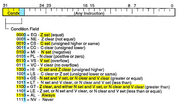
The ARM manual excerpt below shows how four bits in each 32-bit instruction specify one of 16 conditions. Most of the conditions are straightforward, checking if values are equal, negative, higher, and so forth. Most instructions will use the "always" condition, which simply means the instruction always executes. The opposite "never" condition is not highly useful - an instruction with that condition never executes - but it can be used for a NOP, patching code, or adjusting timing of an instruction sequence.
Studying the different conditions reveals much of how the condition circuit works. It is based on four condition flags. The zero (Z) flag is set if a value is zero. The negative (N) flag is set if a value is negative. The carry (C) flag is set if there is a carry or borrow from addition or subtraction. The overflow (V) flag is set if there is an overflow during signed arithmetic (details).
The top three bits of the instruction select one of eight conditions, as highlighted in yellow. The fourth bit selects the condition or its opposite (blue). If the fourth bit is 0, the condition must be true; if the fourth bit is 1, the condition must be false.
Implementation of the circuit
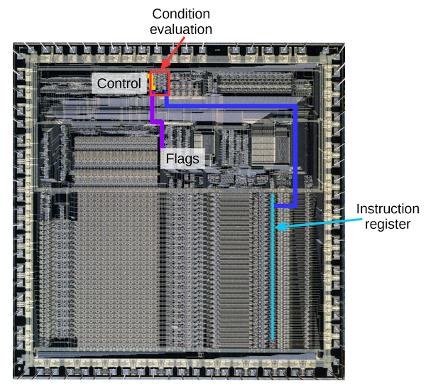
The implementation of the conditional logic circuit matches the above description. First, the eight conditions are generated from the four flags. One of the conditions is selected based on the three instruction bits. If the fourth instruction bit is set, the condition is flipped. The result is 1 if the condition is satisfied, and 0 if the condition is not satisfied. One unexpected part of the circuit is that an undefined instruction or and interrupt causes the condition to be cleared, preventing execution of the instruction. The resulting condition signal output is connected to a control part of the chip, where it causes the instruction to be executed or not, as desired.
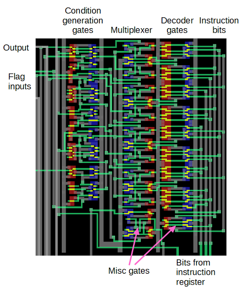
The diagram above shows the condition code circuit of the chip as it appears in the simulator; this is a zoomed-in version of the red rectangle indicated on the die earlier. The chip consists of multiple layers, indicated by different colors. Transistors appear as red or blue regions. NMOS transistors are red; they turn on with a 1 input and can pull their output low. PMOS transistors (blue) are complementary; they turn on with a 0 input and can pull their output high. Physically above the transistors is the polysilicon wiring layer (green). When polysilicon crosses a transistor it forms the gate (yellow) that controls the transistor. Finally, two layers of metal wiring (gray) are above the polysilicon.
The circuit is arranged in columns. The first column of transistors forms the logic gates to generate the conditions from the flag values. The next column is the multiplexer, a circuit that takes the eight input conditions and selects one. The rightmost column contains 8 NAND gates that decode the three instruction bits into 8 control lines. Each line is fed into the multiplexer to select the corresponding condition. At the right is the wiring for the 3 instruction bits and their complements. A few miscellaneous gates are at the bottom of the multiplexer and decoder columns. These include inverters to complement the instruction bits.
The condition generation gates
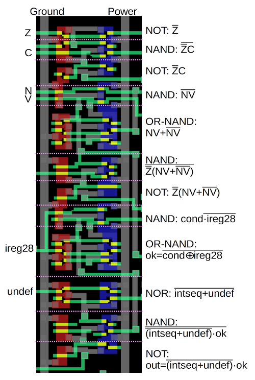
The diagram below zooms in on the left third of the circuit above. This part of the circuit uses standard CMOS logic gates to computes the conditions from the flags. Each gate is built from NMOS (red) and PMOS (blue) transistors in a horizontal strip. Comparing the text description of conditions from the manual with the logic shows how the conditions are generated. For instance, the HI (unsigned higher) condition requires flags "C set and Z clear". The top three gates generate this condition. The GE (greater than or equal) condition is more complex, requiring flags "N set and V set, or N clear and V clear". The next two gates compute this value. (Due to the way CMOS gates are constructed, an OR-NAND gate is constructed as a single gate.) Likewise, the other conditions are generated. The AL (always) condition is simply a 1, and doesn't require any circuitry. The conditions are fed into the multiplexer, which will be discussed below.
The output coming back from the multiplexer is the selected condition, labeled "cond" below. The NAND and OR-NAND gates flip the condition if instruction register bit 28 (ireg28) is set. This implements the eight opposite conditions. The result is labeled "ok", indicating the overall condition is satisfied. The final three gates block instruction execution for an interrupt or undefined instruction.
One thing I'd like to emphasize about the ARM1 is that its layout is very orderly and non-optimized. While it may appear chaotic, the gates are arranged by combining relatively fixed blocks ("standard cells") and wiring them together. Each gate forms a strip and the gates are stacked together in columns. The polysilicon and metal layers connect the gates as necessary.
The layout of the ARM1 chip is a consequence of the VLSI Technology chip design software used to create it. The resulting layout is simple, but doesn't use space very efficiently. Since the ARM1 uses very few transistors for its time, the designers weren't worried about optimizing the layout. In contrast, earlier chips such as the Z-80 were hand-drawn, with each transistor and wire carefully shaped to use the minimum space possible. The diagram below shows a small part of the Z-80 processor layout, showing the extremely irregular but dense arrangement of the chip. The transistors are not arranged in rows as in the ARM1 above, but fit together to use all the available space.
The multiplexer and decoders
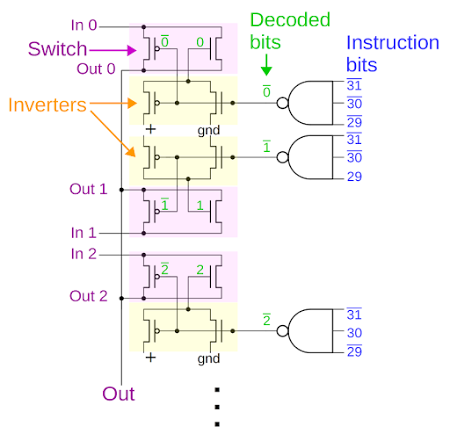
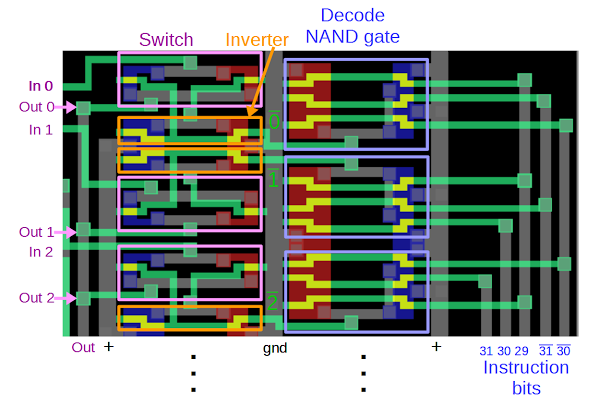
Selecting the desired condition out of the eight possibilities is the job of a circuit called the multiplexer. The multiplexer takes 8 inputs (the conditions) and 8 control signals (based on the instruction) and selects the desired condition. To the right of the multiplexer, 8 NAND gates generate the 8 control signals by decoding the three instruction bits. Each gate simply looks at three bit values and outputs a 0 if the bits select that condition. For instance, if the first two bits are 0 and the third is 1, the gate for condition 1 outputs a 0, selecting that condition in the multiplexer. The animation below shows the circuit as the instruction bits cycle through the eight conditions. You can see the activated condition moving downwards through the circuit.While a multiplexer can be built from standard logic gates, the ARM1 multiplexer is built from a different type of circuitry called transmission gates (which the ARM1 also uses in its bit counter). A multiplexer built from transmission gates is more compact and faster than one built from standard logic (NAND gates). One feature of CMOS is that by combining an NMOS transistor and a PMOS transistor in parallel, a transmission gate switch can be built. Feeding 1 into the NMOS gate and 0 into the PMOS gate turns on both transistors and they pass their input through. With the opposite gate values, both transistors turn off and the switch opens. The multiplexer is built from 8 of these CMOS switches. Each condition input feeds into one switch, and the switch outputs are connected together. One switch is turned on at a time, selecting the corresponding input as the output value.
The diagram below shows the schematic of the multiplexer as well as its physical layout on the chip. Only the first three segments of the eight are shown; the remainder are similar. Each input is connected to two transistors forming a CMOS switch. Because the NMOS and PMOS gates require opposite signals, the multiplexer has an inverter for each control signal. Each inverter also consists of two transistors, but wired differently from the switch.
Working together the decode circuit, inverters, and CMOS switches form the multiplexer that selects the desired condition from the eight choices. The logic described earlier allows this condition to be flipped, for a total of 16 possible conditions.
Conclusion
One unusual feature of the ARM instruction set is that every instruction has a condition associated with it and is only executed if the condition is true. The ARM1 chip is simple enough that the condition circuitry on the chip can be examined and understood at the transistor and gate level. Now that you've seen the internals of the condition logic, you can use the Visual ARM1 simulator to see the circuit in action. While the ARM1 may seem like a historical artifact of the 1980s, ARM processors power most smartphones, so there's probably a similar circuit controlling your phone right now.Thanks to the Visual 6502 team for providing the simulator and ARM1 chip layout data. If you're interested in ARM1 internals, see my full set of ARM posts and Dave Mugridge's series of posts.


No comments:
Post a Comment