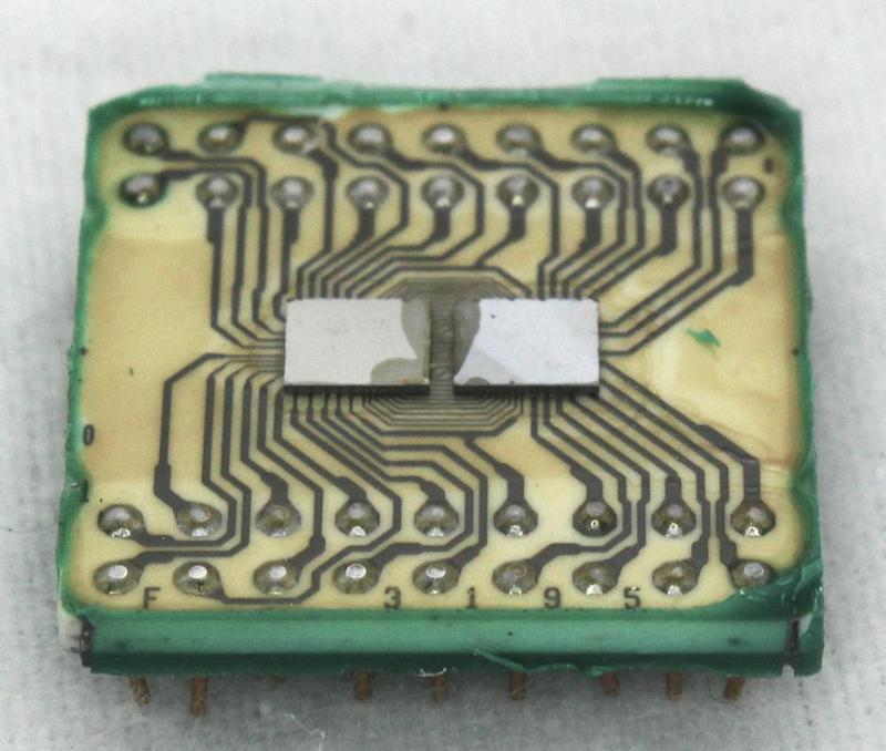
In 1971, semiconductor memory was still a new development so chips couldn't hold a lot of data. To double the storage capacity, IBM used the brute-force approach of putting two silicon dies into a 1-inch square package.1 The photo below shows a module with two face-down silicon dies, storing 4 kilobytes of data. In this blog post, I look inside this package, examine the dies, and explain how this ROM (read-only memory) was implemented. Although I expected the circuitry to be straightforward, the primitive MOS transistors of the time made the circuitry more complicated in several ways.
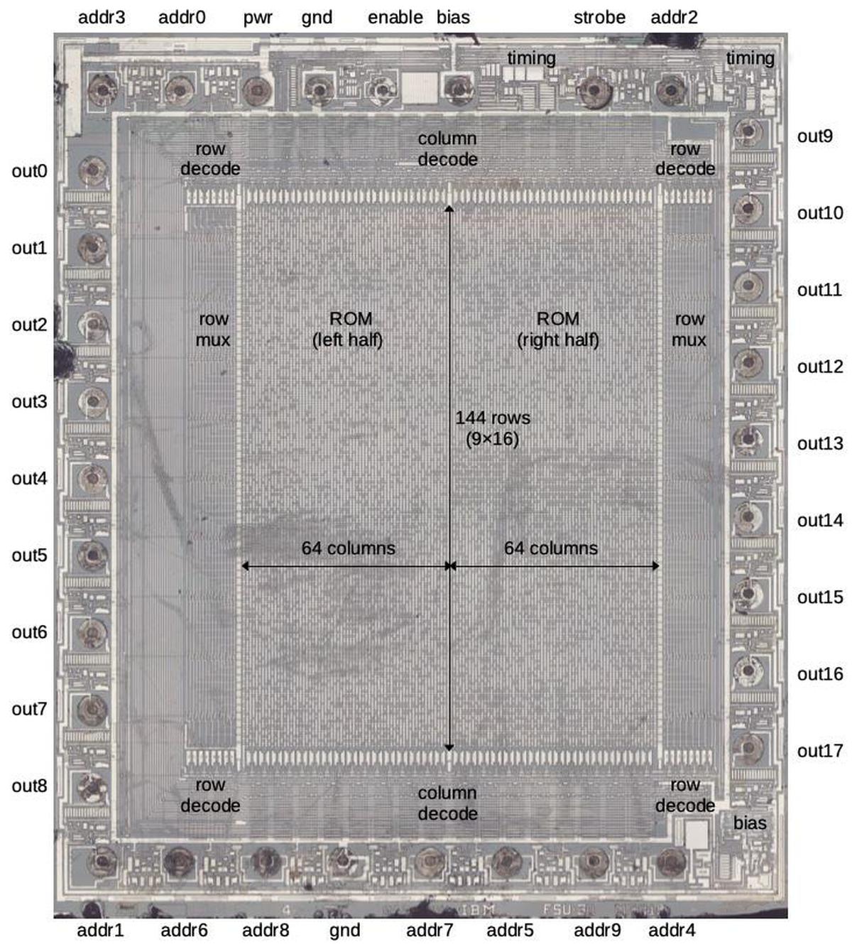
The photo below shows one of the silicon dies under the microscope. The white lines are the chip's metal layer, the wiring that connects the components together. The silicon underneath appears gray. Around the perimeter of the die, the dark circles are the solder balls that connect the die to the ceramic substrate. (Although other manufacturers typically attached tiny bond wires to pads on ICs, IBM soldered the die directly onto the substrate upside down in "flip-chip" style.) The solder balls provide the address lines, output data, and other connections. With 18 output connections, each die stores 1024 words of 18 bits: 9 on the left and 9 on the right. (18 bits may seem like a strange size, but it's a 16-bit word with a parity bit for each byte.2) The data is stored in a matrix of tiny transistors: 128 wide by 144 tall. This matrix is surrounded by the circuitry that selects a particular column and set of rows based on the address, outputting the desired 18 bits.
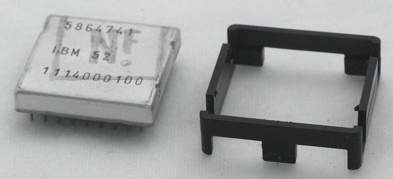
The integrated circuit is packaged in IBM's characteristic square metal can, below. These metal cans have their roots in the IBM System/360, a groundbreaking computer line introduced in 1964. Because IBM didn't consider the technology of integrated circuits to be mature enough at the time, IBM built these computers from hybrid modules called SLT (Solid Logic Technology). These thumbnail-sided modules consisted of individual transistors, diodes, and resistors encased in a square aluminum can. In 1968, IBM moved to integrated circuits (which they called Monolithic System Technology or MST), but kept the metal-can packaging. These packages gives vintage IBM boards a unique look, unlike the rectangular black epoxy integrated circuits used by most manufacturers.
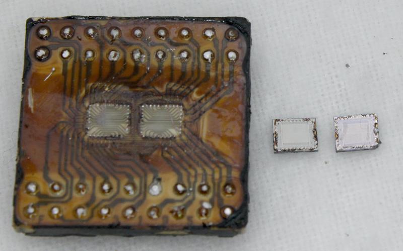
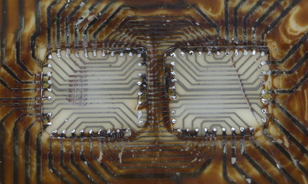
To get inside the package, I removed the metal lid from the package with a hacksaw, exposing the two dies inside. To loosen the dies from the substrate, I used a butane torch to melt the solder connections.3 The photo below shows the dies next to the substrate. As you can see, the varnish on the substrate got a bit toasty during the removal process.
Looking at the substrate closely shows the complex wiring between the pins and the dies. The two chips are wired in parallel, with the substrate wiring connecting corresponding pins on the two dies. The exception is the three pins on the left side of each die near the bottom; they are wired separately to the two dies so one die can be selected.4 You can also see the tiny pads where the solder balls on the dies were attached.
Transistors in the chip
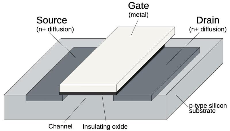
Next, I'll explain the construction of the chip, starting with the transistors that form its circuitry. The dies use metal-gate MOS transistors, an early type of MOS transistor that was largely replaced by silicon-gate transistors in the 1970s. The diagram below shows the construction of a metal-gate NMOS transistor. At the bottom, two regions of silicon (dark gray) are doped to make them conductive, forming the source and drain of the transistor. The gate is formed by a metal strip between the silicon regions, separated from the silicon by a thin layer of insulating oxide. (These layers—Metal, Oxide, Semiconductor—give the MOS transistor its name.) The transistor can be considered a switch between the source and drain, controlled by the gate. To simplify the behavior, the transistor turns on when the gate is pulled positive, and turns off when the gate is at 0 volts.5
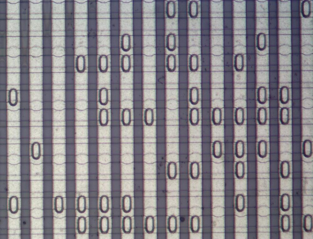
In the closeup of the ROM below, you can see the individual bits. Each oval-shaped "bubble" is a transistor, representing a 1 bit. The vertical white stripes are the metal layer. The faint horizontal stripes are doped silicon. A "bubble" is formed by a thin spot in the oxide where the metal is close enough to the silicon to form a transistor gate. (Elsewhere, the thicker oxide layer separates the metal from the silicon so it doesn't have any effect.) These different layers were created by photolithography, projecting light through a patterned mask and then treating the silicon wafer with chemicals. The contents of the chip are fixed during manufacturing and cannot be changed. Since the mask defines the contents of the ROM, it is called a "mask ROM".
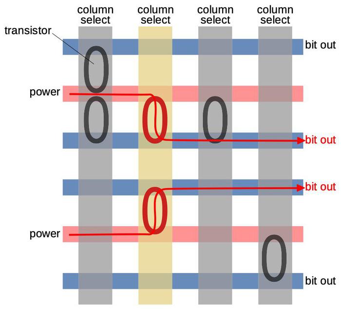
The diagram below explains the structure of the ROM. Each vertical metal line selects a column of transistors; there are 128 vertical lines in total. The ovals indicate transistors: each transistor is between a power line and a bit output line, and its gate is formed by the metal column select line above it. To read the ROM, one column is activated by pulling it high (yellow). This turns on the transistors (red) in that column. An activated transistor connects the corresponding bit output line to power, pulling it high.
The matrix produces 144 bits of output on each side of the chip. To select the desired 9 bits, a circuit called a "16-to-1 multiplexer" selects one bit out of each group of 16. To summarize, part of the address fed into the chip is used to select a column, and part of the address is used to select the output bits. Together, the address selects one of the 1024 words stored on the die.
Construction of an inverter
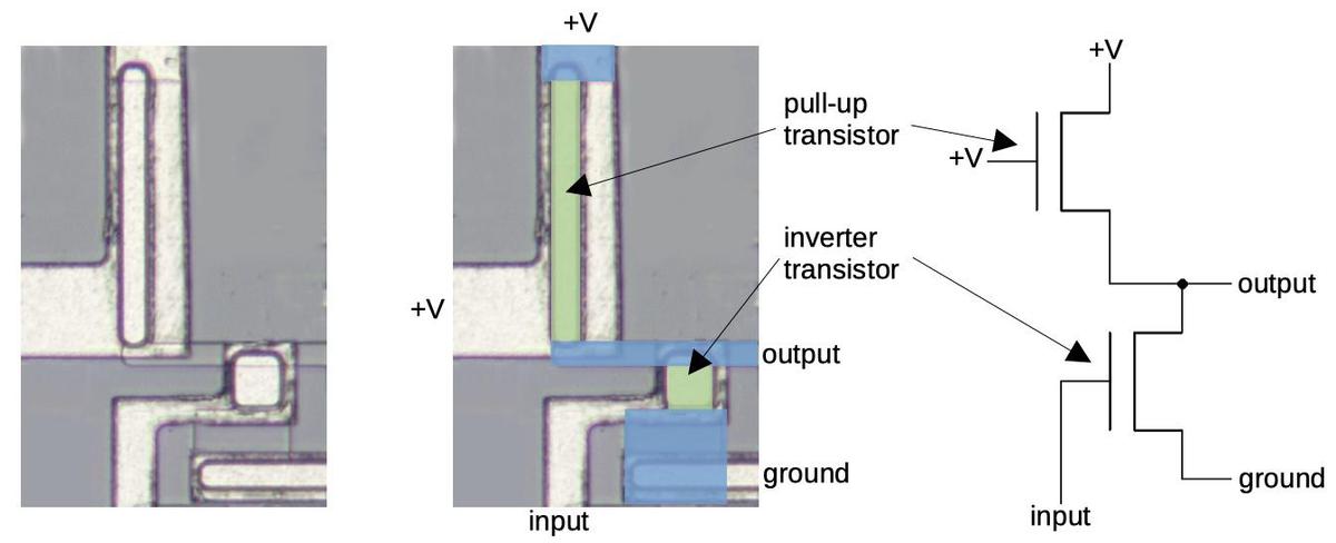
Next, I'll explain some of the logic circuitry. An inverter is the simplest logic gate, used in several places in the chip. The diagram below shows how a basic inverter appears on the die. The metal wiring (white) covers the silicon underneath. The middle diagram shows the conductive silicon in blue, while the transistors are colored green. The inverter is formed from two transistors: a pull-up transistor and a transistor I'll call the inverter transistor. These transistors are controlled by the metal wiring on top of them, which forms the gate.
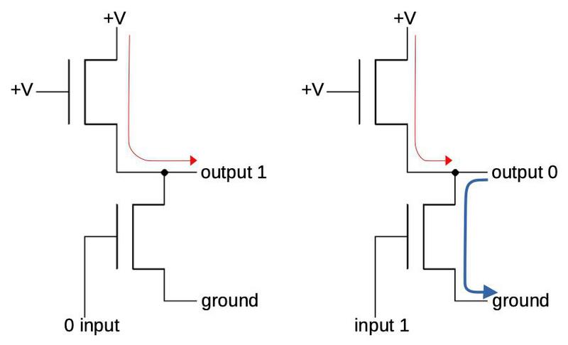
The diagram below shows how the inverter operates. When the input is low (left), the pull-up transistor provides a weak current to pull the output high. (Because the transistor is long and narrow, its current is weak.) When the input is high (right), the lower transistor turns on, connecting the output to ground, resulting in a 0 output. Since this circuit produces a 1 output for a 0 input and vice versa, it acts as an inverter.
This inverter doesn't perform very well because these early metal-gate transistors had difficulty pulling the output high. The problem is that the transistor produces an output voltage that is 4 volts lower than the gate voltage due to the properties of the transistor. Thus, if the inverter above is powered with 10 volts, the output voltage will be just 6 volts, not 10.
The solution was the "bootstrap load" shown below: adding a capacitor and a third transistor to the inverter.6 The capacitor acted as a charge pump, boosting the voltage across the gate and thus the output voltage. The circuit is a bit tricky, but I'll try to explain it. In the first panel, a 1 input turns on the lower transistor, producing a 0 output as before. However, the upper transistor will charge the capacitor with 6 volts, which will be important in the next step.
Next, suppose we input a 0 to the inverter (middle panel). The pull-up transistor on the right will pull the output to 6 volts, as in the simple inverter. But here's the trick: the capacitor was previously charged to 6 volts, so if we raise the lower side of the capacitor to 6 volts, the high side now rises to 12 volts (because of the 6 volts stored in the capacitor). With 12 volts on the gate, the output transistor can produce 8 volts of output. This extra 2 volts will raise the capacitor even higher, giving more output voltage. This feedback loop continues, until the capacitor reaches 16 volts and the output reaches 10 volts. (The output can't get any higher than the 10 volts supplied to the transistor.) Thus, the output transistor has "pulled itself up by its bootstraps", reaching a nice 10-volt output, rather than the weak 6-volt output from the simpler inverter.
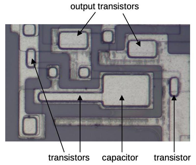
The diagram below shows an inverter on the die, with 5 transistors and a capacitor. This inverter has a bootstrap load, along with two output transistors to boost the current.7 The capacitor is constructed from a large region of metal over silicon: the metal and silicon form the two plates of the capacitor and hold the charge. Note the large size of the capacitor compared to the transistors. This diagram illustrates that even an inverter required a lot of circuitry when using the primitive transistors of 1971.
Column address decoding
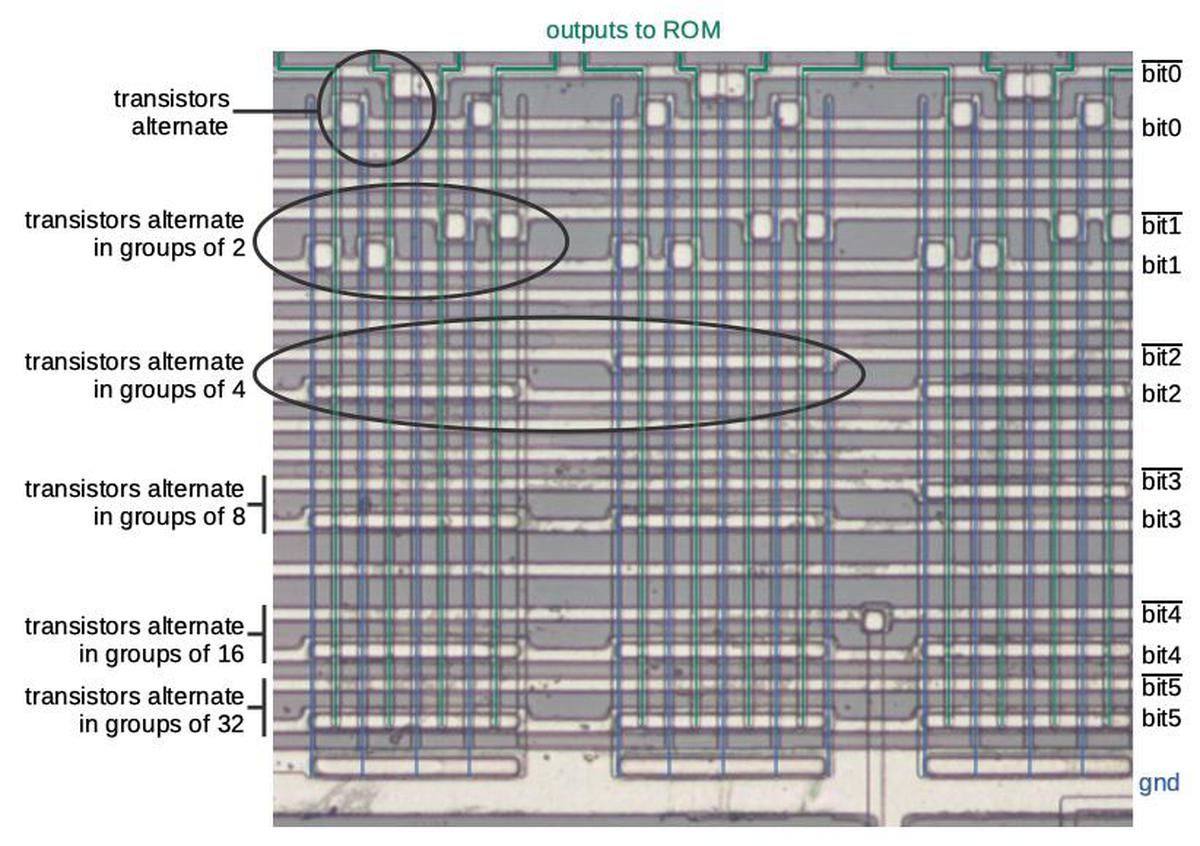
The next circuit I'll describe is the address decoder, which selects the desired column of the ROM based on the input address. Specifically, 6 bits of the address are used to select one of 64 columns. The decoder takes up a fair amount of area on the die, with half the decoder above the ROM matrix and half below. The interesting thing about the decoder is that you can see its binary structure, with two rows of transistors that alternate, then two rows that alternate in groups of 2, groups of 4, and so on.8
Each vertical green line above is one decoder output, corresponding to one particular address. Electrically, each decoder line is wired as a NOR gate: if the line to any transistor is high, the transistor turns on, connecting that output line (green) to ground (blue), pulling it low. If all the corresponding address lines are low, the transistors will remain off, and that column will be activated. Each column of the decoder matches one address bit pattern, so each address selects the desired column.
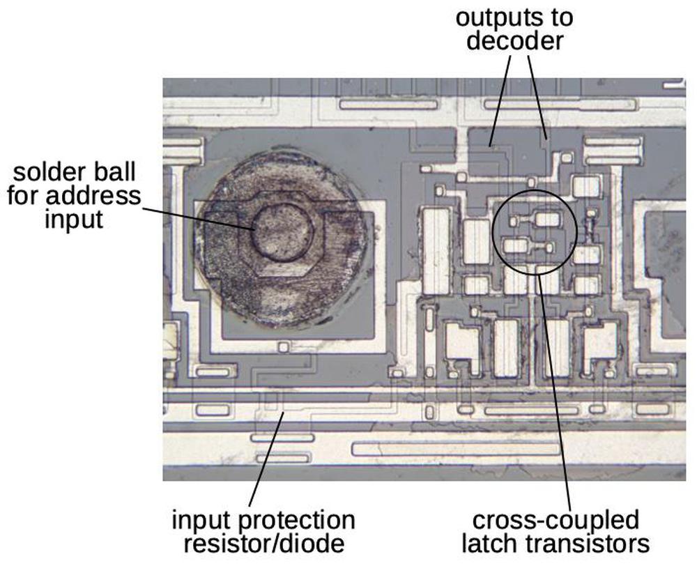
Each horizontal line (and complement) that are fed into the decoder are driven from one of the address inputs. Next to each address input is the circuit below that drives these lines, as shown below. I won't go into details, but it's essentially a latch driven by the address input, outputting the value and its complement.
Row multiplexer circuit
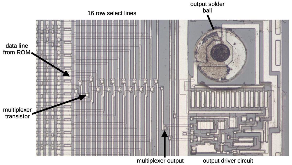
While you might expect each column of the ROM to store one word, the result would be a very tall and skinny ROM that wouldn't fit on the IC die. Instead, each column of the ROM holds 16 words, making the ROM a more efficient rectangle. These 16 words are grouped by bit: the 16 values for bit 0 at the top, followed by the 16 values for bit 1, and so forth. Each output bit has a multiplexer circuit that selects one of these 16 values based on four bits of the address.
Each multiplexer circuit consists of 16 transistors, shown below: one row-select line is activated, turning on the appropriate transistor and connecting that ROM line to the multiplexer output, and thus the output pin. (The row select lines come from a decoder circuit similar to the column address decoder described earlier.) The output driver circuit amplifies the ROM output. Note the large output transistor below the solder ball. Its multiple vertical stripes are multiple gates, allowing it to produce more current for the external signal.
The substrate bias generator
To improve the performance of the transistors, many chips applied a negative "bias" voltage to the silicon die's substrate. The straightforward way to obtain this bias voltage was through an external pin, but this inconveniently required an additional power supply. The IBM ROM chip, instead, has a circuit to generate the negative bias voltage internally, avoiding the extra power supply.9
This substrate bias generator circuit uses a charge pump to create the negative bias voltage from the positive supply voltage, which is a neat trick. The idea is to "pump" electric charge in and out of a capacitor, analogous to a water pump, making the substrate negative. First, the capacitor is charged with 10 volts. Next, the upper side of the capacitor is grounded to 0 volts. Since the capacitor still holds a charge of 10 volts, the lower side of the capacitor must be at -10 volts, producing the desired negative voltage. This cycle is repeated at high speed, driven by an oscillator.
In more detail, the diagram above shows the charge pump driven by a pulse signal and its complement. In the first stage, the two smaller transistors are turned on, charging the capacitor to +10 volts. In the second state, the large lower transistor is turned on, grounding the left side of the capacitor. This forces the right side of the capacitor to -10 volts, pulling the substrate negative. The diode prevents current from flowing back into the substrate during the first stage.
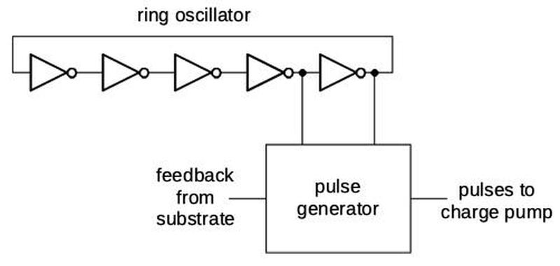
The circuitry that drives the charge pump is shown below. Five inverters are connected into a ring, forming a ring oscillator. If the first inverter has a 1 input, it outputs a 0, so the second outputs a 1, and so forth, until the final inverter outputs a 0. This goes back into the first inverter, flipping its output to 1, and so forth, until the final inverter flips to a 1 output. The process repeats, causing an oscillation. The pulse generator circuit uses these oscillations to drive the charge pump. It also takes a feedback signal from the substrate, stopping the charge pump when the substrate is sufficiently negative.
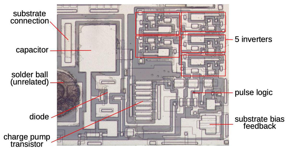
The diagram below shows how the substrate bias generator is implemented on the die. The five inverters are on the right, while the charge pump circuitry is on the left. (These inverters are implemented using the inverter circuit described earlier.) The large capacitor, transistor, and diode for the charge pump are the most visible features.
Optional circuitry
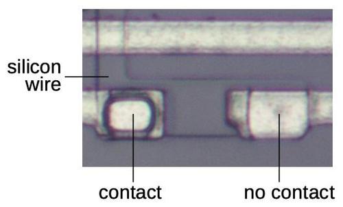
One interesting characteristic of the chip is that some transistors are not implemented and some wiring connections are omitted. In the diagram below, the metal wire on the left has a contact with the silicon, but the metal wire on the right doesn't have a contact; it just overlaps. With a small change to the mask during manufacturing, the contact can be switched to the other wire. This swaps the function of the two inputs in the upper right corner of the chip, strobe and address. (I'm not sure why this is useful, though. Maybe backward compatibility with two different chips?)
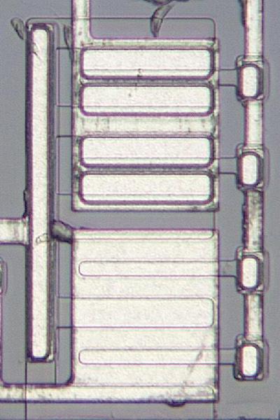
To support that functionality swap, the chip also has unimplemented transistors, as shown below. The upper block has the "bubbles" that indicate working gates. The lower block has the silicon and metal layout of a transistor, but without the gates this circuitry is inert. With a small mask change, the chip can be manufactured with transistors in the lower block and the upper block unused. The point is that the chip was designed so different versions of the chip could easily be manufactured.
Conclusion
The 1970s were a time of great change for integrated circuits. Chips based on MOS transistors were rapidly growing in capability, leading to the rise of microprocessors, semiconductor storage, and other applications. But in 1971, the performance of these transistors was still limited, requiring inconvenient workarounds such as capacitors for bootstrap loads. The density of chips was also limited, causing IBM to put multiple dies in one package to store enough data.
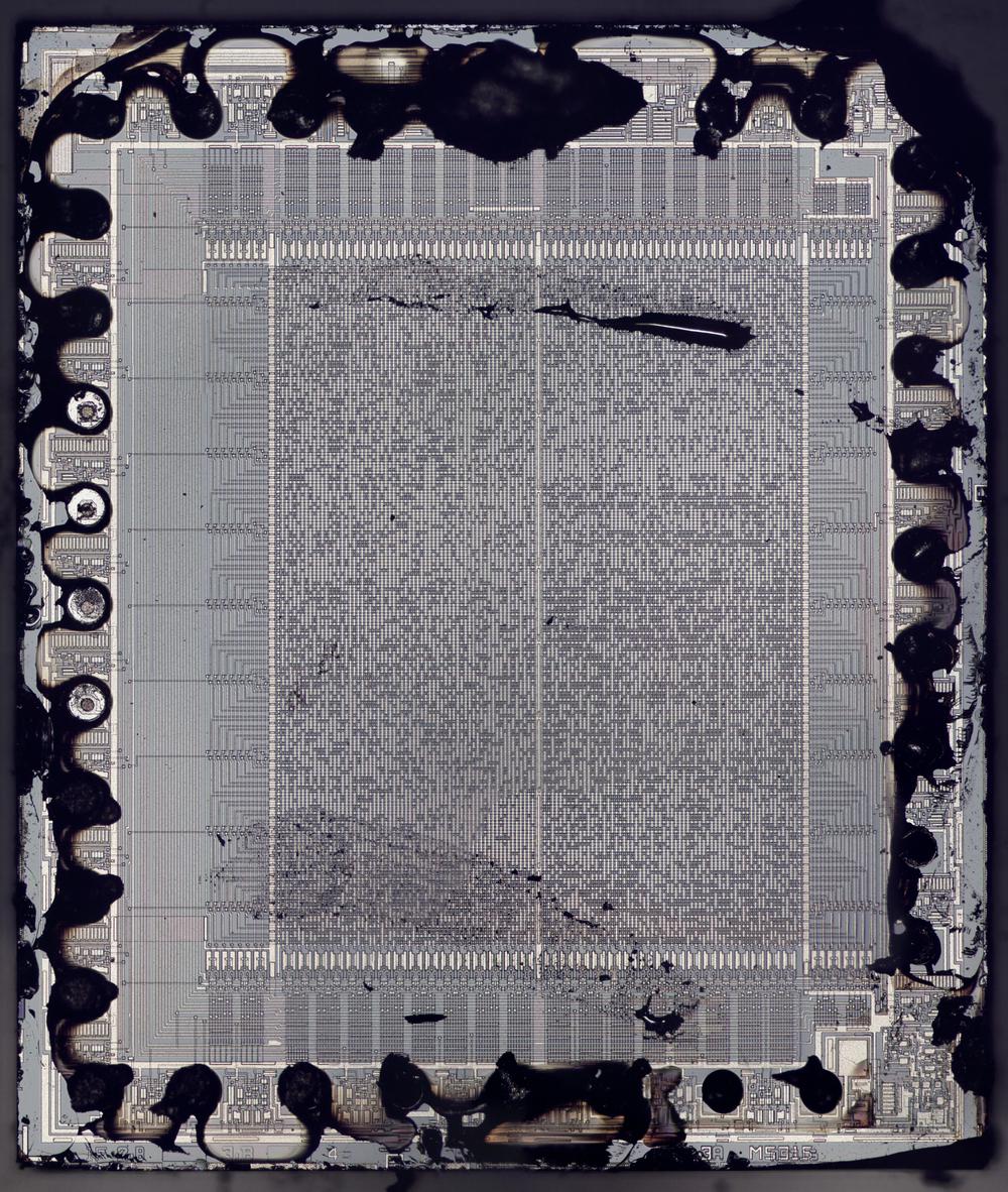
Looking at this package, both dies are the same, except for the data stored on them. The photo below shows the other die that was in the package. The black globs are some sort of varnish that covered the dies and leaked in around the edges. I couldn't find anything that dissolved the varnish, so I ended up tediously chipping it off under a microscope. (This is why the cleaned die photo at the beginning of the post has some scratches.)
What does the ROM hold? Unfortunately, I don't know. I'm told that it comes from some type of IBM printer so it's probably some sort of interface firmware.
I announce my latest blog posts on Twitter, so follow me @kenshirriff. I also have an RSS feed.
Notes and references
-
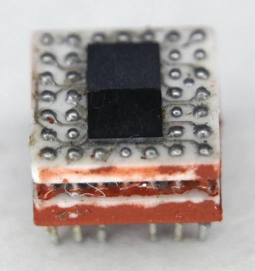
IBM often put multiple silicon dies in a single package, especially to increase memory density. Since the capacity of a single die was limited by the silicon technology at the time, packaging multiple dies together was a straightforward way to increase density. The memory module below shows four silicon RAM dies mounted on two layers of ceramic.
An 8-kilobit IBM memory module containing four 2-kilobit chips on two levels. More details here. -
I checked some of the data in the ROM to verify that the "extra" bits were parity. I confirmed that each 9-bit chunk had odd parity, an odd number of 1 bits. ↩
-
I have disassembled several IBM modules. In most cases, heating the ceramic substrate with a heat gun is sufficient to melt the solder and release the dies. However, the ROM dies were apparently covered with varnish that held them securely, and the heat gun was not sufficient to remove them. Lacking a propane torch, I used a crème brûlée torch which provided enough heat to get the chips off the substrate. The substrate ended up blackened and started smoking in the process, however. At least I didn't need to barbecue the module. ↩
-
Each die has 34 solder balls, while the package has 36 pins (4 rows of 9), so I'll explain how the math works out. Most of the pins are connected in parallel to each die. Ground, however, is connected twice to each die. Each die also has 3 pins that are connected separately, allowing the die to be addressed individually. Thus, the package has 30 pins that are shared across the die, and 6 pins that are connected 3 to each die. ↩
-
Since I have no information about this chip, everything is from reverse-engineering and I had to make some guesses. I want to be honest about what parts are speculative, so I'll summarize in this footnote. I don't know if the chip uses NMOS or PMOS transistors since they look the same under the microscope. Given the early date of this chip, it's very possible that it used PMOS transistors. If so, the explanation of the chip is essentially the same, except the voltage levels are reversed and negative. I illustrate many of the circuits with a supply voltage of 10 volts; I don't know the actual voltage used by these chips. Likewise, the 4-volt threshold voltage is an assumption. The output labels 0-17 are arbitrary since I can't tell what order the bits are in. The labels on the address bits are based on the decoder patterns but I don't know if data was stored row-first or column-first. I'm speculating that a transistor in the ROM indicates a 1 bit, but it could indicate a 0 bit. The explanation of the strobe and enable inputs is based on examining the circuit, but could be wrong. ↩
-
The transistor's output voltage is lower than desired due to the large "threshold voltage" of early metal-gate transistors. The transistor turns on when the gate voltage is sufficiently higher than the drain (output) voltage. This voltage difference is the threshold voltage, which could be several volts. The workaround is to raise the gate voltage a few volts higher to overcome the threshold voltage. I've written about the bootstrap load in the Intel 8008 processor (link) if you want more information about bootstrap loads. ↩
-
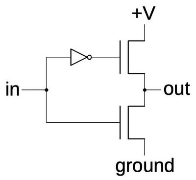
The bootstrap load produces a higher-voltage output than can be obtained directly. The higher voltage can be traded off to obtain a high-current output. The trick is to use two more transistors to produce the final output, as shown below. The upper transistor, fed by the inverter, pulls the output high, while the lower transistor, fed by the original input, pulls the output low. The point of this is it takes five transistors and a capacitor to produce a good inverter. In comparison, just a couple of years later, semiconductor technology had advanced so only two transistors were required.
Adding two output transistors provides a higher-current output for the inverter. -
A few things to note about the column decoders. First, half the decoders are at the top of the ROM and half are at the bottom of the ROM. This is because the decoders are about twice as wide as a ROM cell so they wouldn't all fit on one side of the ROM. Second, the decoders are duplicated for the left and right sides of the ROM since the left and right sides provide two bytes for the same address. (It was more space-efficient to duplicate the decoders than to use one set of decoders with 64 wires between the two sides of the ROM.) Third, if you look carefully, the first rows of transistors don't alternate in the pattern "ABAB ABAB" (as you'd expect for binary), but instead alternate "ABBA ABBA". Thus, the columns are accessed in the order 0, 1, 3, 2, and so forth, instead of the order 0, 1, 2, 3. This is invisible to the user of the ROM, as long as the columns are shuffled appropriately when the ROM is programmed. ↩
-
Curiously, the IBM ROM chip has a pin that appears to be tied to the substrate to provide bias, as well as an on-chip bias generator I don't know why the chip would have both. If you want more information about substrate bias generators, I've written about the substrate bias generators in the 8086 and 8087.
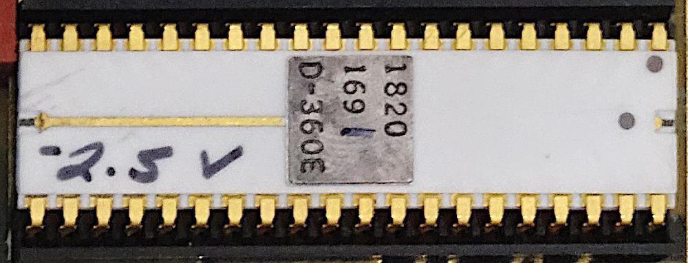
The bias voltage of the Hewlett-Packard Nanoprocessor was unusual. Due to variability in the manufacturing process, the bias voltage varied from chip to chip. During production, each chip was tested and the proper bias voltage was hand-written on the chip. Each circuit board had to be adjusted to provide the necessary bias voltage.
The HP Nanoprocessor. Note the hand-written voltage "-2.5 V". The last digit (1) of the part number is also hand-written, indicating the speed of the chip. Photo courtesy of Marc Verdiell.


3 comments:
s/durin /during /
Great work as usual. The crème brûlée torch, nice touch!
Great work!
All I can say is "Hats-Off" for empowering us with your work. More power to you. Keep us enlightening with your work.
Post a Comment