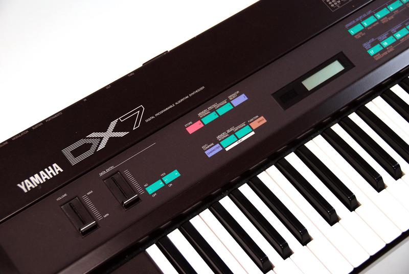
The Yamaha DX7 digital synthesizer (1983) was the classic synthesizer in 1980s pop music. It uses a technique called FM synthesis to produce complex, harmonically-rich sounds. In this blog post, I look inside its custom sound chip and explain how the chip's output circuitry works. You might expect it's just a digital output fed into a digital-to-analog converter, but there's much more to it than just that.
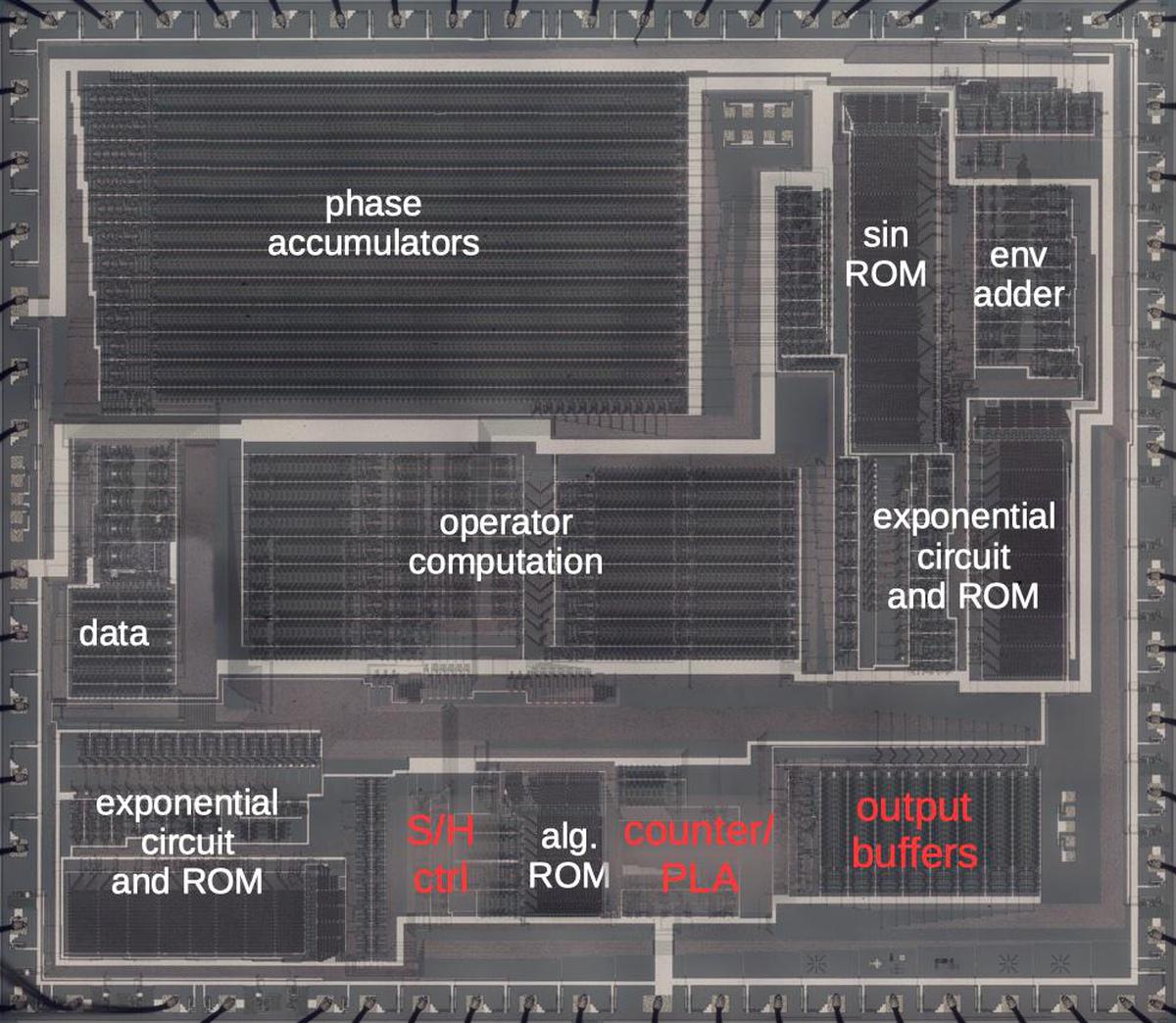
The composite die photo above shows the DX7's OPS sound synthesis chip under the microscope, revealing its complex silicon circuitry. Unlike modern chips, this chip has just one layer of metal, visible as the whitish lines on top. Around the edges are the 64 bond wires attached to pads; these connect the silicon die to the chip's 64 pins. The three blocks in red are the focus of this post. The output buffers hold the 16-bit digital values for the 16 notes. The output is controlled by a counter and PLA (Programmable Logic Array). The synthesizer's digital-to-analog conversion uses a sample-and-hold circuit, controlled by the "S/H ctrl" block.
I've discussed the chip's other functional blocks in earlier posts1, so I'll just give a brief summary here. Each of the 96 oscillators has a phase accumulator used to generate the frequency. The oscillators are combined using the operator computation circuitry in the middle of the chip, under the control of the algorithm ROM. The signal synthesis uses sine and exponential functions, implemented with lookup tables in ROMs.
The synthesizer's output circuitry
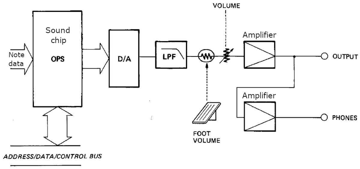
Before I dive into the details of the chip, I'll explain the synthesizer's output circuit. The heart of the synthesizer is the OPS (Operator S) sound chip that digitally generates the notes. It provides digital values to the digital-to-analog converter (D/A). The resulting analog signal goes through a low-pass filter (LPF). The volume is controlled by a foot pedal and the synthesizer's volume control. Finally, the signal is amplified for the line and headphone outputs.
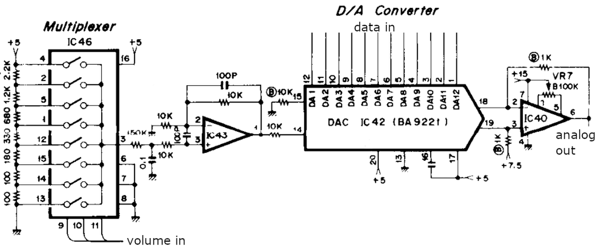
The digital-to-analog conversion is more complex than you might expect. The process starts with the digital-to-analog converter (DAC) chip2 that takes a 12-bit digital value from the sound chip and converts it to an analog value in the range 0 to 15 volts.3 The multiplexer allows the overall synthesizer volume to be controlled by MIDI, but with just 8 levels.
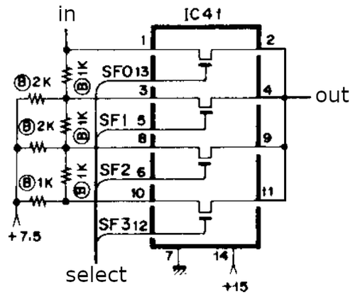
The DAC provides 12 bits of resolution, but an additional circuit (below) provides approximately two more bits. This scaler circuit divides the analog signal by 1, 2, 4, or 8, using a resistor network and IC switch. The scaler is controlled by the sound chip through the scale factor signals SF0-SF3. The scaler adds more dynamic range to the digital value; the result is similar to a floating-point value with a sign bit, 11-bit mantissa, and two-bit exponent.4
Next, the signal goes to a sample-and-hold circuit that samples the analog voltage at a point in time and holds it in a capacitor, kind of like an analog memory. An op-amp buffers the capacitor's voltage so it can be "read" without draining the capacitor. There are two hold circuits, used in alternation, so the last two samples are stored and summed to form the circuit's output.5 The SH1 and SH2 control signals load the analog value into a capacitor, using IC52 as a switch. Finally, the output from the sample-and-hold circuit is filtered,6 the volume is adjusted,7 and the signal is amplified for the output (circuitry not shown).
To summarize, the sound chip interacts with the output circuitry in three ways. The 12-bit digital value (DA1-DA12) is most important as it specifies the output value for each voice. The scale factor signals (SF0-SF3) are also a key contributor to the signal. The sound chip also provides the sample-and-hold control signals (SH1 and SH2).
Time-division multiplexing
The DX7 has 16 voices, so it can play 16 notes at once. Each note is produced by an "algorithm" that combines 6 oscillators in a particular way, so there are 96 oscillators in total. An oscillator can modulate the frequency of another oscillator to generate complex sounds with FM synthesis.
The chip performs all its processing sequentially, one oscillator at a time, rather than computing the notes in parallel. Internally, the chip has one "operator" calculation circuit to combine oscillators. As shown below, the chip starts by processing operator 6 for note 1, then operator 6 for note 2, and so forth through note 16. Then it processes operator 5 for notes 1 through 16. Finally it processes operator 1 for notes 1 through 16, generating the output sound values. It takes a bit over 20 µs to compute all 16 notes in a complete processing cycle.
You might expect the chip to combine the 16 notes into a single digital output. However, the sound chip outputs the 16 notes sequentially, using a technique called time-division multiplexing. Each time interval (~20µs) is divided into 16 intervals and one note is output from the chip per interval. (Note that these intervals don't line up with the intervals in the diagram above.) Thus, digital values are output at 786 kilohertz, 16 times the underlying frequency, and the DAC chip converts them to analog at this rate.
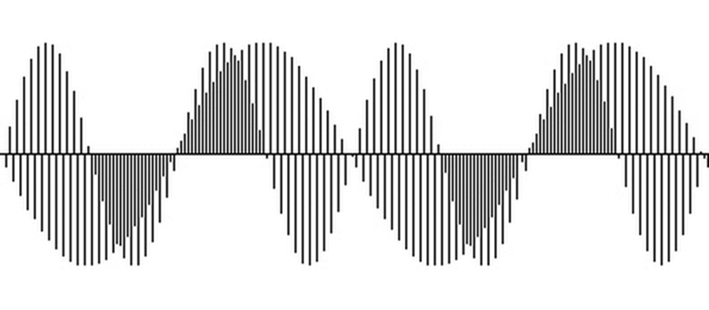
As an example, consider two notes that are sine waves with different frequencies. The digital output would look like the image below. You might think that this signal is unusable since it jumps around wildly from point to point.
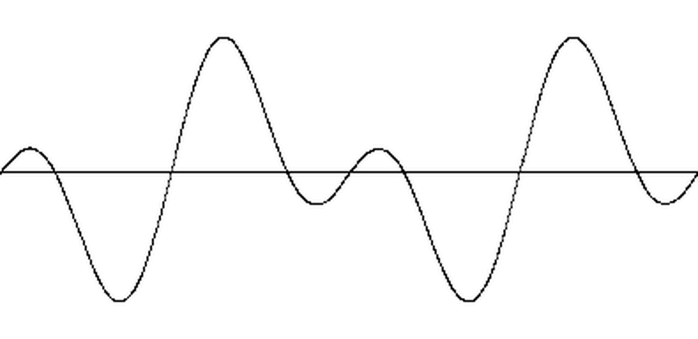
However, applying a low-pass filter smooths out the waveform (essentially summing nearby points). The result is the waveform below, which shows the sum of the two sine waves.8 The point is that time-division multiplexing data may look strange, but the analog circuitry's filtering creates a "normal" waveform.
Output buffer
Inside the chip, the output buffer stores values for the 16 notes as they are generated, and outputs them in sequence. Rather than RAM, the chip uses shift registers for storage. The shift registers are arranged in a loop of 16 stages, one stage for each note. On each clock cycle, the values in the shift register move to the next stage. The output value is fed back into the shift register's input so the value is retained. Alternatively, a new value can be stored in the shift register. Shift registers provided an efficient way to store data, but they cannot be accessed arbitrarily; instead, data must be processed as it becomes available.
The schematic below shows how one stage of the shift register is implemented. The chip uses a two-phase clock. In the first phase, clock ϕ1 goes high, turning on the first transistor. The input signal goes through the inverter, through the transistor, and the voltage is stored in the capacitor (kind of like DRAM). In the second phase, clock ϕ2 goes high, turning on the second transistor. The value stored in the capacitor goes through the second inverter, through the second transistor, and to the output, where it enters the next shift register stage.
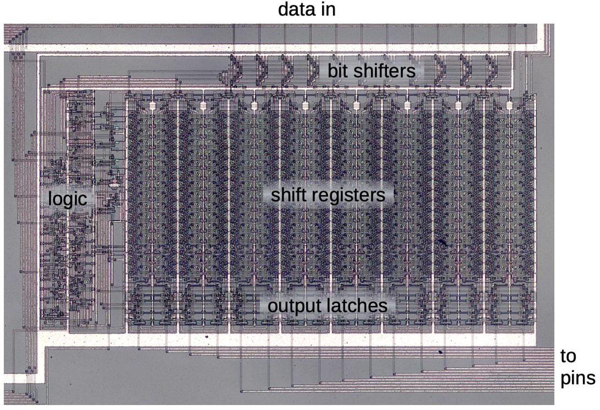
The die photo below shows the output buffer, with the 16 shift-register loops arranged in columns. These hold the 16-bit sound values (four scale factor bits and 16 data bits.) Each shift register is 16 stages long to hold the 16 notes. In the next sections, I'll discuss the bit shifters, the logic, and the output latches.
The scale factor: pseudo floating point
The DX7 uses a 12-bit digital-to-analog converter chip, but the scaling circuit (discussed earlier) will scale the voltage by 1, 2, 4, or 8, which adds more resolution. This isn't quite equivalent to 14-bit resolution; it's more like a floating-point number with a sign, 11-bit mantissa, and 2-bit exponent. This provides more resolution for low signals and reduces signal noise.
Inside the chip, scaling is implemented with a shifter that shifts the data bits by 0 to 3 bit positions. (This is unrelated to the shift registers that hold data.) The shifter (below) is implemented as eleven chevron-shaped logic gates; each gate selects one of four potential bits for each mantissa position.
The operator circuitry generates data as 15 bits (2's complement, so one of the bits provides the sign). The output from the chip is 12 bits, so three bits must be discarded. Normally these are the low-order bits, but by using the shifter, high-order zero bits can be discarded instead, and the external scaler counteracts this. The result is more bits of precision in the output.
The shifter is controlled by the logic circuitry to the left of the buffer, which controls the amount of shift based on the number of leading zeros. (For a negative number, leading 1's.) With 5 leading zeros, the number is shifted left by 3 positions. With 4 leading zeros, the number is shifted by 2 positions. With 3 leading zeros, the number is shifted by 1 position. With 2 or fewer leading zeros, the number is unshifted.
Note that the circuit leaves two leading zeros when it shifts, so it's "wasting" two potential bits of precision. I assume this is because the scaler won't be perfectly linear (due to the resistor imperfections9), so you want to avoid switching scale levels for large signals (which don't really need the extra bits).10
The output latches
As mentioned earlier, the 16 notes are output individually, spaced across the interval. This timing doesn't line up with the timing of the output buffer, which shifts to a new note every clock cycle. To fix the timing, two 16-bit latches sit between the output buffer and the output pins. While one latch outputs the current note, the other latch grabs the next note as it is shifted out of the shift register. At the appropriate time, the latches swap roles; the second latch outputs the note while the first latch waits for the next note.
The timing for the latches is fairly tricky to make sure the note data is loaded into the right latch at the right time. These latches are controlled by the chip's master counter, which is the subject of the next section.
To summarize, the sound chip runs at 4.7 MHz. Data values are produced at this rate (but intermittently) and stored into the output buffer. The output latches provide data values to the DAC chip at 786 kHz for an overall audio rate of 49096 Hertz.
Keeping track of 96 clock cycles: the chip's counter and timing PLA
One complete cycle of the sound chip takes 96 clock cycles: processing all 16 notes through the 6 operators that form an algorithm. Because data can only be accessed when it exits a shift register, everything must be timed so the right data is available at the right time. A critical part of the chip is the counter that keeps track of the current note number and operator number to keep everything synchronized.
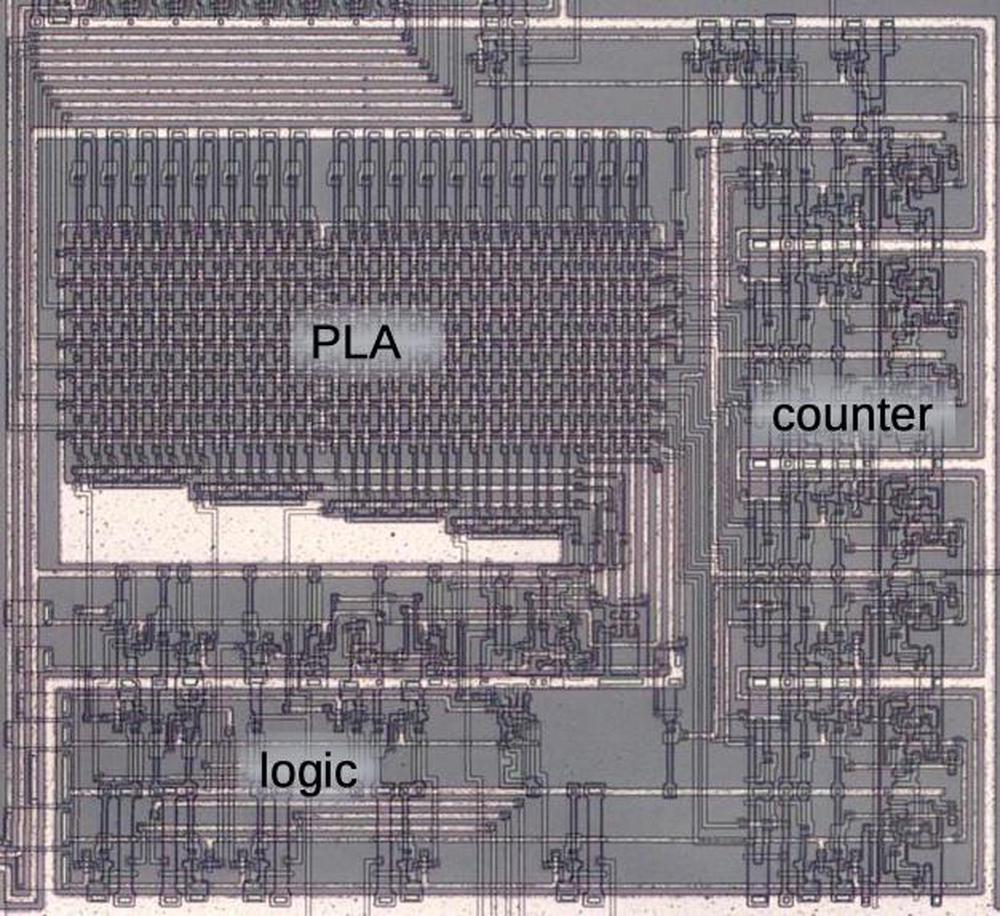
On the right of the die photo below is the counter, consisting of seven toggle flip flops: four to count the note number (0-15) and three to count the algorithm number (0-5). On the left is the PLA that defines what happens for particular time slices. (A Programmable Logic Array (PLA) is similar to a ROM, but implements arbitrary logic.) The PLA has 39 columns, each one implementing an AND gate triggered by a particular counter output, corresponding to a particular operator and note. Below the PLA is some logic; mostly buffers with a few gates.
Of the PLA's 39 columns, the 32 columns on the left control the data output latches,11 two columns control loading data values into the output buffer, one generates the chip's sync output signal, three reset the operator count, and the last increments the operator count.12
Sample-and-hold
The chip outputs two signals to control the sample-and-hold circuitry, SH1 and SH2. These signals are activated in alternation to take an analog sample of each digital output.
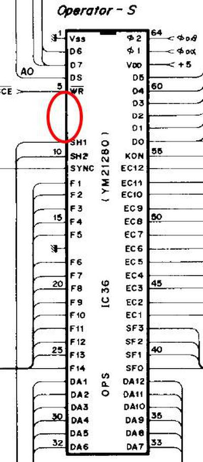
The sound chip has three unused pins next to the SH1 and SH2 pins; the DX7 schematic doesn't show pins 6-8. I traced the chip's internal circuitry and found that these pins, in conjunction with the sample-and-hold pins, count out the 16 samples. It appears that the chip is designed to sample-and-hold all 16 notes individually, so the synthesizer could have had separate outputs for all 16 notes.13
Moreover, the chip has data buffers to hold separate algorithm algorithms for the 16 notes. This would let the chip drive 16 independent voices, each with a separate algorithm. My conclusion is that the sound chip supports much more flexibility than is used in the DX7 synthesizer.
Conclusion
The DX7 generates sounds digitally and then converts the digital values to the analog output. This process turns out to be more complicated than one would expect, with circuitry inside the chip interacting with synthesizer circuitry to scale and adjust the signal. My hope is that my analysis of this process will help DX7 emulators to achieve more accuracy. Looking at the chip's internal circuitry reveals the floating-point format of the output data as well as the function of the three unused pins.
I plan to continue investigating the DX7's circuitry, so follow me on Twitter @kenshirriff for updates. I also have an RSS feed. Thanks to Jacques Mattheij and Anthony Richardson for providing the chip and discussion.14
Notes and references
-
My previous posts on the DX7: DX7 reverse-engineering, The exponential ROM, The log-sine ROM, and How algorithms are implemented. ↩
-
The DAC chip is the BA9221, a 12-bit D/A converter that produces an output current based on a 2's-complement input value. A datasheet is here. The DAC receives an input voltage reference. This voltage reference can be one of 8 values selected by a multiplexer. This allows the overall volume to be set via MIDI, but only with 3-bit resolution (see the DX7 ROM code here). The volume is an exponential function (so linear in decibels) except that 0 is off. Also see this DAC discussion and this StackExchange discussion.) ↩
-
The output from the DAC is centered around 7.5 volts. In other words. a digital value 0 corresponds to 7.5 volts, with positive digital value above 7.5 volts and negative digital values below 7.5 volts. I would have expected the signals to be centered around 0 volts, which is what the DAC datasheet shows. I think strictly positive voltages were used because they work better with the TC4066 and TC4066 integrated circuits switches (IC 41 for scaling and IC 52 for sample-and-hold respectively). The DX7 converts the signals to zero-centered voltages for the low-pass filter. ↩
-
The amplitude scaler is built from an R-2R resistor ladder, similar to a DAC circuit. However, the attenuator only has 4 useful values, not the 16 levels you might expect with four control lines, because only one control line can be activated at a time. Combinations of control lines do not yield useful outputs. For example, if the top switch is on, you get the maximum output regardless of the other switches. Other switch combinations are non-monotonic. Thus, the scaler only provides two additional bits of resolution, not four. ↩
-
The benefit of keeping two samples is not clear to me. One theory is that this reduces intermodulation distortion between the voices, the effect of one signal on another. With one "solid" sample and one changing sample, the effect of the changing sample will be reduced. Another, more speculative, possibility is that the circuitry was originally designed for stereo, holding one sample for each channel. ↩
-
The filter is a sharp low-pass filter around 16 kHz using a Sallen-Key topology. ↩
-
The volume is controlled by an external volume pedal and a volume control on the synthesizer. The signal also passes through a relay, which cuts the output when the synthesizer is being reset (presumably to avoid random noise).
The external volume pedal has an interesting circuit. The pedal is essentially a variable resistor, so you might expect the output signal to pass through it. Instead, the pedal is connected to a photocoupler with an LED and a cadmium sulfide photocell inside. The output signal passes through the photocell and is attenuated as controlled by the LED. I think the motivation behind using a cadmium sulfide photocell instead of a phototransistor is that the photocell is completely resistive, so there is no nonlinear distortion of the signal. ↩
-
Time-division multiplexing and filtering isn't perfect, and will contribute some artifacts to the output. In particular, there will be some aliasing, where high frequencies turn into lower frequencies. The low-pass filter will eliminate most of the high frequencies—I believe the DX7's filter is at 16 kHz—but it's not perfect and will add its own color to the sound. Two notes could also interact differently based on their relative positions in the time slice. These artifacts probably contribute to the DX7's characteristic sound. You could consider the artifacts desirable if you're trying to duplicate the DX7 sound. ↩
-
The scale resistors are marked on the schematic with Ⓑ, which probably indicates they are higher-precision resistors. Assuming they are 1% resistors, a 1% error in a large signal would be much more error than the benefit of additional bits of precision. For smaller signals, the additional bits reduce the quantization noise, which is probably more important than the nonlinearity error from scaling. ↩
-
There's an interesting timing issue for the scale calculation. The scaling logic requires about 3 clock cycles to determine the scale factor, so the straightforward implementation would shift a voice based on the amplitude of an earlier voice. The solution is that the 5 bits for scale calculation are pulled out of the operator shift register six stages (3 clock cycles) earlier. Thus, these shift registers have two output; the "early" output gives the scale factor circuitry time to work. ↩
-
The output buffer has two latches, used by alternating notes. Each latch has one control line to latch a data value and one control line to output the latched value, so there are four control lines in total. Curiously, it appears that the notes aren't output sequentially; the order is 1, 13, 5, 11, 3, 15, 7, 10, 2, 14, 6, 12, 4, 16, 8, 9. I don't know if there's a motivation for this; it's also possible that I'm misinterpreting the circuit. ↩
-
A few notes on the PLA outputs in case anyone looks at them more closely. Because signals get delayed through multiple shift registers and clock cycles, things don't happen on the cycle you'd expect. For instance, SYNC is generated 6 cycles before the end. Likewise, loading of the output buffer is triggered midway through operator 6, about 26 cycles later than operator 1 started generating outputs. Most PLA columns are triggered for a specific voice and operator value. The exception is the last column, which increments the operator regardless of the operator value. Curiously, there are three counter reset lines. One resets near the end of operator 1 (as you'd expect). The other two reset near the end of the two invalid operator values (there are 6 operators but 8 possible bit values). Presumably this keeps the synth from starting up in a bad state. Below the PLA are some gates. These are mostly buffering and clock synchronization. ↩
-
Someone with a DX7 could probe the three unused pins and verify that they count out the notes. ↩
-
For more information on the DX7 internals, see DX7 Technical Analysis, DX7 Hardware, OPLx decapsulated, and the video Emulating the DX7 the hard way. ↩




5 comments:
Brilliant stuff
Regarding the foot pedal, I would guess that they use a photocell instead of a potentiometer for longevity and smoothness of input. A stage floor is a cruddy place, and feet are cruddy things, and potentiometers full of crud tend to crackle and fail. A photocell might require cleaning from time to time, but it won't fail as quickly or as noisily.
@The Clue Merchant:
That's not what this means; the photocell is in the DX, NOT in the pedal. The pedal itself is a typical TRS "control pedal" with a potentiometer; its not a TS "volume pedal" through which the audio signal is passed (Morley pedals would be such optical volume pedals).
My guess is that the photocell can easily "smooth out" some of the potential pedal "crackle".
About the scale resistors marked "B" (note 9): Those are 0.1% precision according to the DX1 and DX5 service manuals. So I'd assume that this is also true for the DX7.
Posting for David Willmore:
Regarding footnote 5, it's bad practice to run a signal (audio or otherwise) through a potentiometer. The reason being they are noisy devices that tend to get worse with age. Common practice is to sample a voltage off of them, low pass filter that, and then use that value to modulate whatever it is you wanted to control. Running a signal through a pot is asking for all kinds of bad failure modes with age.
Additionally, another reason not to run the signal through a pot in this design is that running an audio signal down to a pedal and back up exposes it to induced noise--power hum, static discharge, electrical fields from motors, etc. That's another reason to condition control signals coming from long wire runs.
The LED/CdS cell gives an inherent low pass filtering due to the slow response of the CdS cell itself. Sounds like the Yamaha engineers knew a thing or two because they had seen a thing or two.
Post a Comment