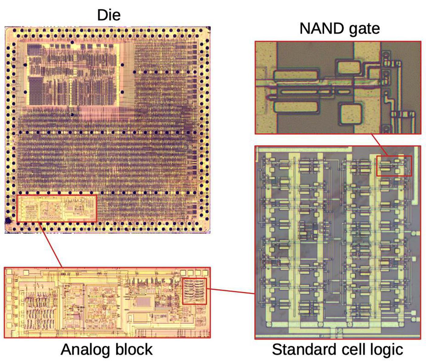
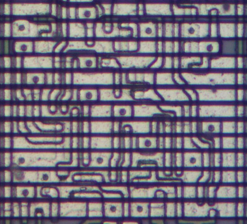
Integrated circuits are often built from standard-cell logic, constructed from standardized building blocks such as NAND gates. Since I've been looking at a chip that uses standard-cell logic, I figured it was a good opportunity to examine standard-cell logic closely by reverse-engineering a simple block of logic on the chip. (It turned out to be a divide-by-16 module.) The diagram below shows the die from an IBM token ring chip from 1993. The chip contains a block of analog network circuitry, but curiously the analog block contains some standard-cell digital logic. Finally, zooming in shows one NAND gate in the logic.
Standard cells let automated tools design a complex integrated circuit from a description in a language such as Verilog. These tools select the appropriate cells from a cell library, place them in rows, and route the wiring between the cells to create the desired logic. This is much easier than a fully-custom design with each individual transistor arranged on the die.1 Vendors supply a library of standard cells2 as well as software to create the design.3 While a library may contain hundreds of different types of cells, the circuit I examined only uses five different cell types, which I will explain below.
The chip
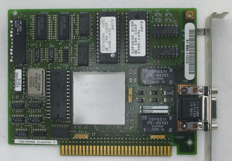
I'll give a brief overview of the chip first, before I scare everyone off with CMOS circuit diagrams. The chip is the large (1.5") square integrated circuit on the board below, packaged in IBM's unusual shiny aluminum can. This chip is the controller for this token ring network board. (I recently wrote about a different token ring IC; the current post describes an older (but related) IC on a different token ring board.)
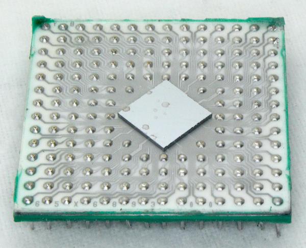
Removing the metal lid from the IC exposes the silicon die inside. The die is mounted upside-down on a ceramic substrate, connected to 175 pins by thin traces on the substrate. Instead of bond wires, the die is attached by solder balls on its surface.
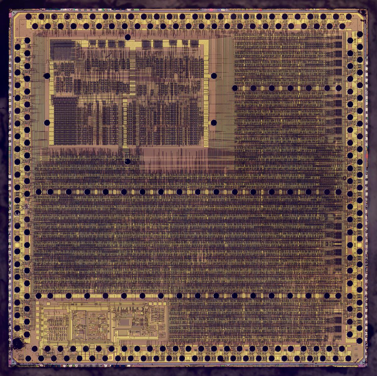
The photo below shows the die under the microscope. The black circles are the solder balls. They form two rows around the perimeter of the die, but there are also rows of solder balls throughout the chip, distributing power and ground.
The chip has two layers of metal wiring: thicker yellowish wires on top and thinner gray wires underneath. The underlying silicon appears pinkish in this photo. Brownish polysilicon wiring is also visible on top of the silicon. Most of the chip consists of rows of standard-cell logic, about 24,000 gates.4 The chip contains a custom microprocessor in the upper left corner. In the lower-left is an analog block that interfaces to the network.5 This block contains a small amount of digital standard-cell logic, which is what I'll describe below.
How CMOS logic is implemented
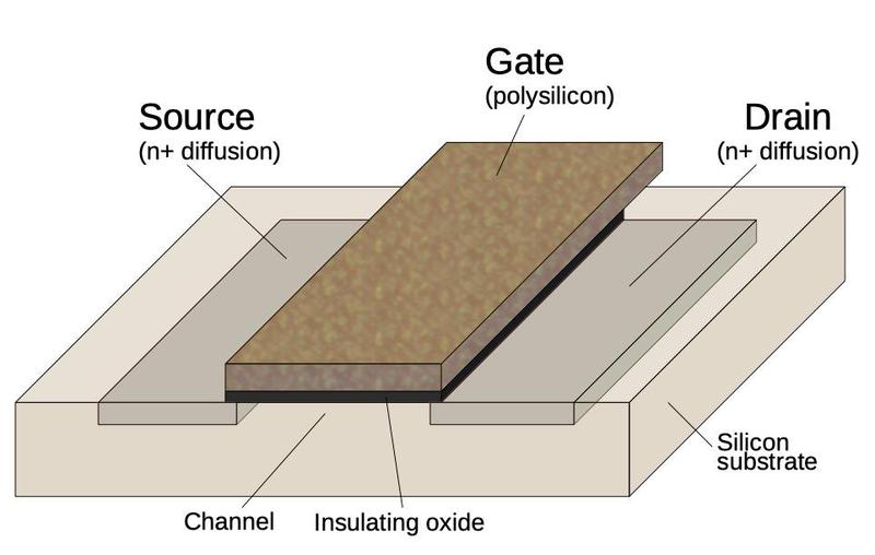
The chip is built with CMOS logic (complementary MOS), which uses two types of transistors, NMOS and PMOS, working together. The diagram below shows how an NMOS transistor is constructed. The transistor can be considered a switch between the source and drain, controlled by the gate. The source and drain (gray) consist of regions of silicon doped with impurities to change its semiconductor properties and called N+ silicon. The gate consists of a special type of silicon called polysilicon, separated from the underlying silicon by a very thin insulating oxide layer. The NMOS transistor turns on when the gate is pulled high.
A PMOS transistor has the opposite construction from NMOS: the source and drain consist of P+ silicon embedded in a substrate of N silicon. The operation of a PMOS transistor is also opposite from the NMOS transistor: it turns on when the gate is pulled low. Typically PMOS transistors pull the drain (output) high, while NMOS transistors pull the drain low. In CMOS, the transistors act in a complementary fashion, pulling the output high or low as needed.
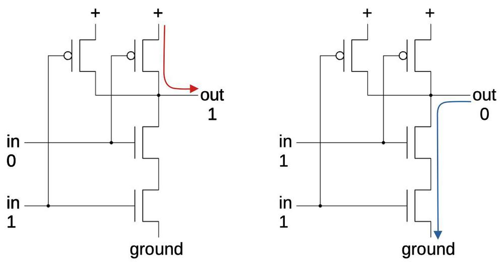
The diagram above illustrates how a CMOS NAND gate works. The gate consists of two PMOS transistors at the top and two NMOS transistors at the bottom. The first case shows what happens when an input is 0. The corresponding PMOS transistor turns on, pulling the output high. In the second case, both inputs are 1. The NMOS transistors turn on, pulling the output to ground, creating a 0 output. Thus, the circuit implements the NAND function.
By removing one input and the corresponding pair of transistors, this circuit becomes an inverter. By adding additional inputs and pairs of transistors, this circuit can be extended to create a NAND gate with 3 or more inputs. Note that the PMOS transistors (on top) are wired in parallel, while the NMOS transistors (on the bottom) are wired in series; this will be important for the standard cell layout.
The standard cell circuits
The circuit block that I'm examining uses five different types of standard cells (out of the hundreds in the library). In this section, I'll show the construction of each cell type, starting with the 2-input NAND gate, and then the more complex cells. Each cell is constructed as a rectangle that fits between the power rails, with inputs and outputs in a line at the bottom. This standard cell layout allows the gates to be arranged into rows without worrying about the internal construction of the cells. The cells can then be wired together, using the chip's two layers of metal wiring.
NAND
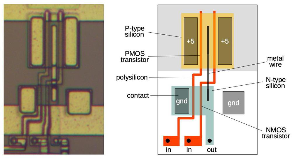
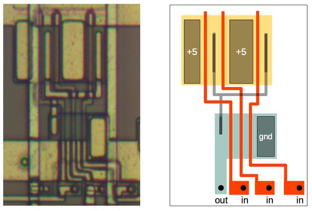
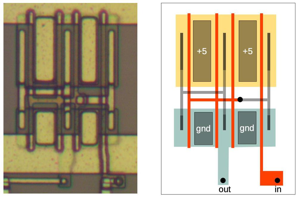
I'll start by examining a 2-input NAND gate cell that implements the NAND circuit described earlier. The photo on the left shows how this NAND gate looks on the die, and the diagram on the right explains the key components. Starting at the bottom, the two inputs are connected to polysilicon wires (red). When these wires cross the N-type silicon (turquoise) at the bottom, they form NMOS transistors. These transistors are connected together by sharing silicon. At the top, when the polysilicon wires cross the P-type silicon (yellow), they form PMOS transistors.6 These transistors are wired in parallel, with one end connected to +5 volts. The metal wire in the middle connects the PMOS transistors to the second NMOS transistor and the output.
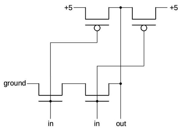
The schematic below shows the transistors arranged to match their physical layout in the cell. If you trace out the paths, this circuit is the same as the NAND circuit described earlier. The structure of the gate is harder to follow in this schematic because the layout is constrained by the needs of the standard cell.
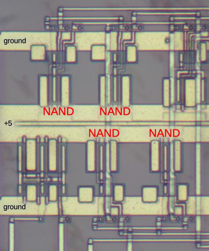
Once we have determined the structure of the NAND gate cell, we can find all the instances of this cell. The diagram below shows a detail of the chip with four NAND gates marked. The gates are identical, except the gates in the top row are flipped because the power wire for them is on the bottom, not the top. (Two other gates in this photo don't match the NAND cell; they will be described below.) Note the two inputs and the output for each of these gates.
The cells are connected together by metal wiring. The chip has two layers of metal. The bottom metal layer is used for the thick horizontal power and ground wiring, the wiring inside each cell, and horizontal wiring between cells. The second metal layer is used for vertical wiring. Much of this vertical wiring passes over cells; because it uses a different layer than the wiring inside the cell, there is no conflict.
3-input NAND
The circuit also uses 3-input NAND gates. The construction is similar to the smaller NAND gate, except there is another PMOS transistor in parallel on top and another NMOS transistor in series on the bottom. While the NMOS transistors are in a nice row, the PMOS transistors require an additional metal wire to connect them in parallel. (The two thick vertical metal wires are not part of the cell.) The schematic is in a footnote for reference.7
4-input AND
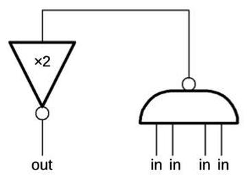
The next gate is more complex: a 4-input AND gate. An AND gate can't be built directly because a CMOS gate requires inversion (because a 1 to the NMOS transistor pulls the output low). Instead, an AND gate is built by inverting the output of a NAND gate, as shown below. In other words, this cell contains two gates.
A second complication is that this gate is constructed to output twice the standard current. It is implemented by using pairs of transistors in parallel in the inverter: two NMOS transistors and two PMOS transistors.8
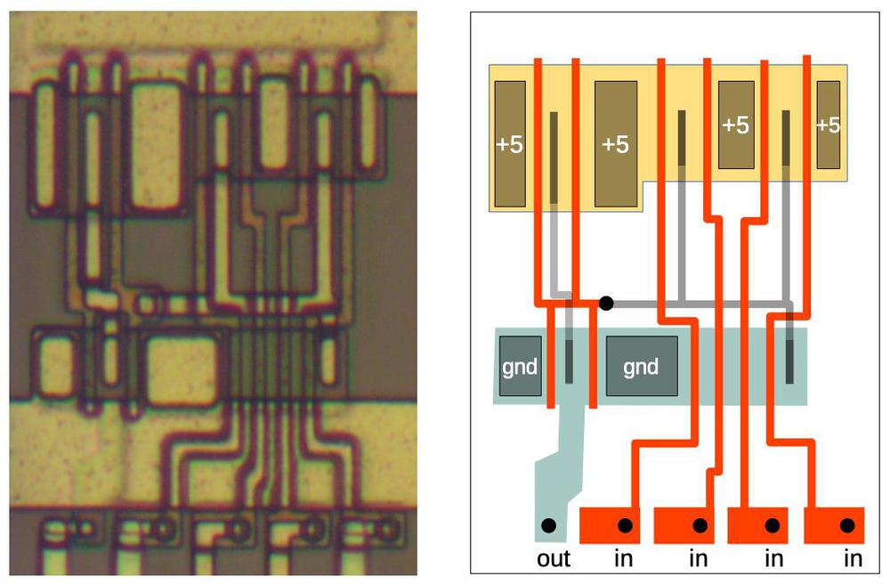
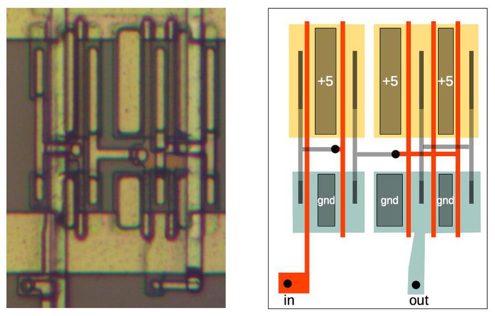
The result of those factors is the 4-input AND gate cell below. On the right side of the cell is a 4-input NAND gate. It is similar to the earlier NAND gates, but with the inputs connected to four PMOS transistors on top wired in parallel and four NMOS transistors on the bottom wired in series. The series transistors are packed together in a tight row, but the parallel PMOS transistors have a more complex layout due to the +5 connections and the wiring to connect them together. On the left is the inverter, driven by the NAND gate's output. The inverter has two pairs of transistors to provide the high-current output. For details, see the schematic in the footnote.9
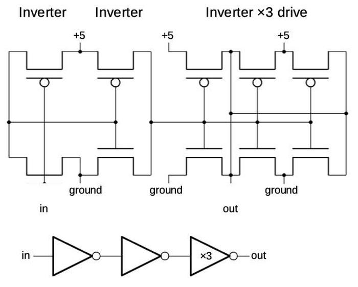
Buffer
Next is a non-inverting buffer with triple-current output, using principles similar to the AND gate. The non-inverting action is achieved by putting the output of an inverter through a second inverter, yielding the original value. The first inverter is on the right, constructed from a PMOS transistor and an NMOS transistor. The output inverter on the left has 3 pairs of transistors to provide high-current output. The H-shaped metal wiring collects the output from the six transistors. The schematic is in the footnote.10
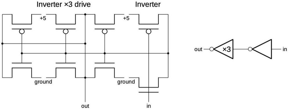
Inverter/driver
The final cell type is an inverter with triple-current output. This could be implemented with a single inverter, but the cell uses three inverters in series. The input goes into the inverter on the left, which is connected to a second inverter in the middle. This drives the inverter on the right, which has three pairs of transistors.11
Reverse-engineering the circuit
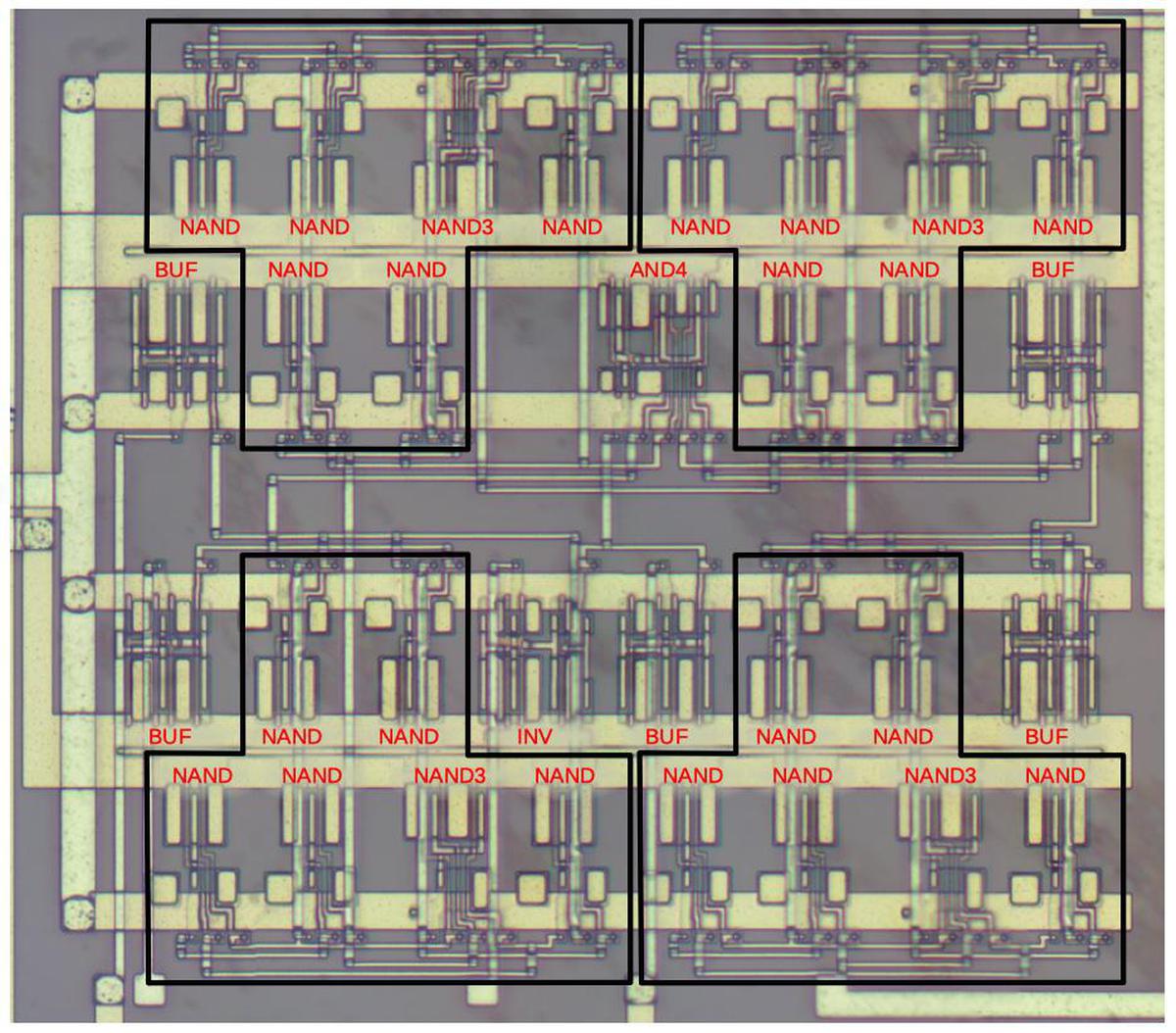
After determining this set of standard cells, each cell on the chip can be labeled with its function, as in the diagram below. Next, tracing out the wiring between the cells reveals how the circuitry is connected. I noticed a repeated motif of six NAND gates connected as cross-coupled latches; these groups are outlined in black.
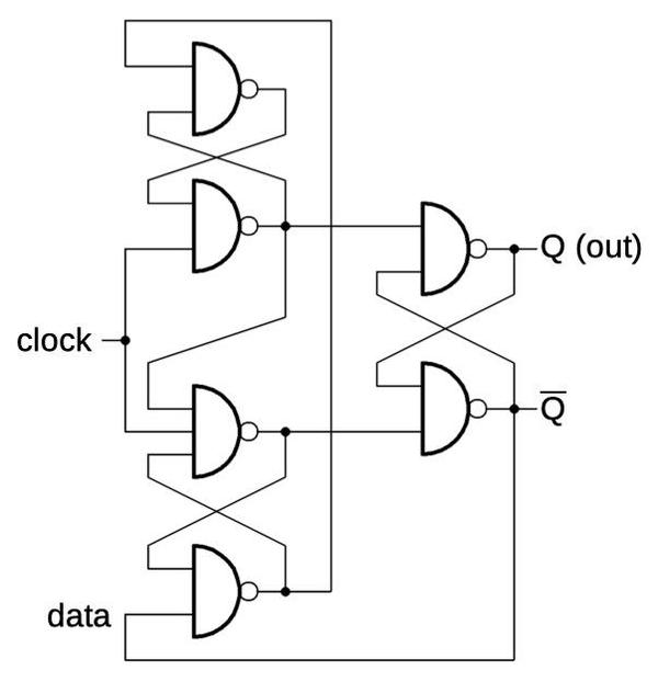
The schematic below shows how these 6-cell blocks are wired. After puzzling over this a while, I realized that this circuit was a standard edge-triggered flip-flop. The idea behind an edge-triggered flip-flop is that when the clock signal goes from 0 to 1, the flip-flop latches the value on the data input and holds it until the next clock transition. In this way, flip-flops provide synchronization and a form of memory and are very useful in many applications. The flip-flop outputs the stored value as Q, and the complement of this value as Q.
In this circuit, the inverted output Q is connected back to the data input, so every clock pulse will cause the flip-flop to toggle between 0 and 1. Since two clock pulses will cause a single 0→1→0 cycle on the output, this flip-flop divides the clock frequency by 2.
With the flip-flops recognized, I could create the schematic for the complete block of logic. The four flip-flops are arranged in sequence to divide the input clock by 16. The four flip-flops are also fed into the 4-input AND gate, which creates a pulse once every 16 clock cycles.12
Conclusion
Standard-cell logic is the mainstream methodology for designing digital logic. In this post, I've reverse-engineered some of the cells used in a vintage IBM chip and determined the circuit implemented by the cells. Although this specific circuit is not very complex, it's interesting to see how standard cells are constructed and how they are used in a real chip. (Although vendors publish specifications of their libraries, it's hard to find details on the physical implementation of the cells.) The chip I examined is from 1993, so its 1µm technology is obsolete compared to modern standard cell libraries that go down to 7 nm and have many layers of metal wiring, but the principles remain the same.
I announce my latest blog posts on Twitter, so follow me @kenshirriff. I also have an RSS feed.
Notes and references
-
You might think that the standard cell layout is not that different from a custom layout. However, a custom layout can be very tightly packed, with transistors winding all over the place. As an example, the photo below shows part of the 8086 processor. Note that the metal lines on top almost completely occupy the available space. The transistors underneath wind around in complex patterns. In addition, the sizes of the transistors are carefully optimized for their role. This is in contrast to standard-cell logic where transistors have a few, fixed sizes. The point is that a custom, optimized layout may be very complicated to achieve as much density as possible.
A closeup of the Intel 8086 die. -
For examples of commercial standard-cell libraries, see AMI's databook (1996) or a Samsung library (2000). ↩
-
IBM's software for synthesizing Boolean logic was called BoolDozer. Papers on it are here and here. ↩
-
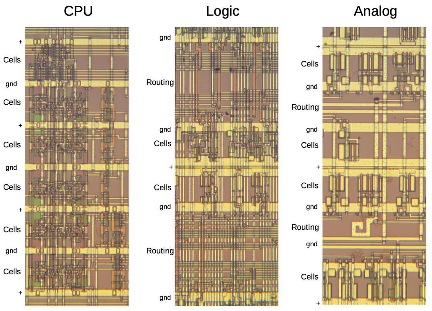
One unusual thing about this integrated circuit is that the CPU, the analog block, and the general logic all use standard cells, but they use different standard cell libraries with completely different layout styles, as shown below. The CPU's standard cells appear to be the densest, with cells between power and ground lines. Horizontal and vertical routing takes place over the cells. The general logic, on the other hand, has larger cells. Wide horizontal bands are used for routing, so only 1/3 of the space contains cells. The logic in the analog block is the least dense. The cells resemble the general logic cells, but larger. The routing wiring is thicker and less dense, looking like little optimization was performed. It's a surprise to find such a variety of standard cell implementations on one chip.
Comparison of standard cells in the CPU, general logic, and the analog block. -
The chip contains a block of analog circuitry implemented in CMOS. This circuitry "performs signal conversion and clock recovery functions as well as detecting and compensating for line impairments". This circuitry includes resistors, capacitors, MOS transistors with special properties, and other components. The analog block uses a variety of circuits such as op-amps, switched-capacitor amplifiers, voltage references, peak detectors, a charge pump, voltage-controlled-oscillator, and phase-locked loop. ↩
-
The PMOS transistors must be embedded in an N-type substrate, while the NMOS transistors must be embedded in a P-type substrate. I suspect that the chip as a whole has a P-type substrate, while the NMOS transistors are in a "tub" of N-type silicon. The substrate doping isn't visible under the microscope, so it could be the other way around. I'm ignoring the substrates in the diagrams. ↩
-
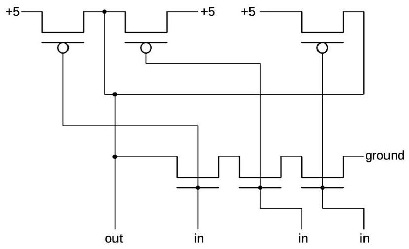
The schematic below shows how the transistors are connected in the 3-input NAND cell. The layout of the schematic matches the physical layout of the cell to make comparison easier. You can verify that the PMOS transistors (top) are in parallel, while the NMOS transistors (bottom) are in series.
Schematic of the 3-input NAND gate. -
Standard-cell libraries typically contain versions of gates with multiple output current levels. A "×2" gate doubles the output transistors, while a ×3 gate has triple output transistors and so forth. Although the different sizes provide flexibility, custom circuitry gives you much more control since transistors can have arbitrary sizes, exactly matching the circuit's need. Typically a gate with higher current output is used if it's driving a long wire or multiple loads. But you don't want to use larger gates unnecessarily, since they have more capacitance and typically take longer to switch. So there are tradeoffs involved. ↩
-
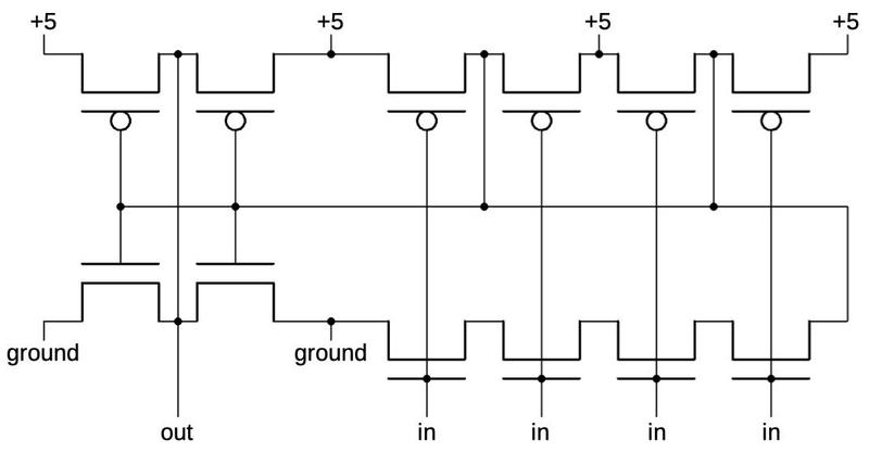
Schematic of the 4-input AND gate with double output drive. It is constructed from a 4-input NAND gate on the right, and an inverter/driver on the left.
Schematic of the 4-input AND. -
The schematic below shows the construction of the non-inverting buffer with triple-current output. It is constructed from an inverter (on the right) feeding a triple-current inverter.
Buffer schematic. -
It may seem strange to use three inverters in series when one inverter has the same logical function, but I think there's an explanation. The triple-current inverter has about three times the input capacitance because of its multiple transistors. Driving this inverter directly would put more load on the gate connected to the input, potentially slowing it down. Adding the two-inverter buffer in front ensures that the cell can be driven with a relatively weak signal.
Schematic of the inverter with ×3 output. -
Interestingly, this divide-by-16 circuit has four outputs, but only two are used. My first thought was that the others are for testing (since they are connected to internal pads). However, these outputs are simply the complements of the other outputs, so they wouldn't provide any testing benefit. The other possibility is that the whole divide-by-16 circuit is a standardized block, used in other applications. ↩

5 comments:
Nice article!
I'm sure that there's a huge difference between the density of custom layout vs standard cell layout (and between different standard cell methodologies as well, it seems).
But your example of custom layout is from the 8086, which is an NMOS chip, unlike this chip, which is CMOS. I believe that the constraint that you have in CMOS to keep NMOS and PMOS transistors separated (while you need both in all gates) makes it harder to squeeze the logic together as tightly as in CMOS. Have you seen any tight custom layout CMOS chips?
I wonder why the metal contacts for Vdd and ground are so much wider than the internal metal wiring used in the gates? Seems like it couldn't be much gain resistance wise at least.
Just started this read and right at the point 3 the IBM logo is mentioned and I would like to share what I saw the other day in Red Hat office.
KR
P
https://www.dropbox.com/s/ulxnb5bguffxyeh/We_are_RH.jpg?dl=0
Fascinating information and great post. The next level engineering is something most people don't expect from that period but this article shows that clearly. Thanks for revealing that to us.
The 63F7704 is the 'Spyglass' - Replaced later by the 'Pinegrove' and 'Pinegrove Shrink' (your other Token-Ring adapter article).
Post a Comment