The Intel 8086 processor was introduced in 1978, setting the course of modern computing. While the x86 processor family has supported 64-bit processing for decades, the original 8086 was a 16-bit processor. As such, it has a 16-bit arithmetic logic unit (ALU).1 The arithmetic logic unit is the heart of a processor: it performs arithmetic operations such as addition and subtraction. It also carries out Boolean logic operations such as bitwise AND and OR as well as also bit shifts and rotates. Since a fast ALU is essential to the overall performance of a processor, ALUs often incorporate interesting design tricks.
The die photo below shows the silicon die of the 8086 processor. The ALU is in the lower-left corner. Above it are the general- and special-purpose registers. An adder, used for address calculation, is in the upper left. (For performance, the 8086 has a separate adder to add the segment register and memory offset when accessing memory.) The large microcode ROM is in the lower right.

Zooming in on the ALU shows that it is constructed from 16 nearly-identical stages, one for each bit. The upper row handles bits 7 to 0 while the lower row handles bits 15 to 8.3 In between, the flag circuitry indicates the status of an arithmetic operation through condition codes such as zero or nonzero, positive or negative, carry, overflow, parity, and so forth. These are typically used for conditional branches.
In this blog post, I reverse-engineer the 8086's ALU and explain how it works. It's more complex than other vintage ALUs that I've studied,2 using a flexible circuit that can implement arbitrary bit functions. The carry is implemented with a Manchester carry chain, a fast design dating back to a 1960s supercomputer.
The ALU circuitry
The 8086's ALU circuitry is a bit tricky, so I'll start by explaining how it adds two numbers. If you've studied digital logic, you may be familiar with the full adder, a building-block for adding binary numbers. Specifically, a full adder takes two bits and a carry-in bit. It adds these three bits and outputs the 1-bit sum, as well as a carry-out bit. (For instance 1+0+1 = 10 in binary, so the carry-out is 1 and the sum bit is 0.) A 16-bit adder can be created by joining 16 full-adders, with the carry-out from one fed into the carry-in of the next.
The simplified diagram below represents one stage of the ALU's adder. It takes two inputs and the carry-in and sums them, forming a 1-bit sum output and a carry-out. (Note that the carry signal travels right-to-left.) The sum bit output is generated by the exclusive-or of the two arguments and the carry-in, using the two exclusive-or gates at the bottom. Generating the carry, however, is more complex.

The carry computation uses an optimization called the Manchester carry chain4, dating back to 1959, to avoid delays as the carry ripples from one stage to the next. The idea is to decide, in parallel, if each stage will generate a carry, propagate an existing carry, or block an incoming carry. Then, the carry can rapidly flow through the "carry chain" without sequential evaluation. To understand this, consider the cases when adding two bits and a carry-in. For 0+0, there will be no carry-out, regardless of any carry-in. On the other hand, adding 1+1 will always produce a carry, regardless of any carry-in; this case is called "carry-generate". The interesting cases are 0+1 and 1+0; there will be a carry-out if there was a carry-in. This case is called "carry-propagate" since the carry-in propagates through the stage unchanged.
In the Manchester carry chain, the carry-propagate signal opens or closes transistors in the carry line. In the carry-propagate case, the top transistor is activated, connecting carry-in to carry-out, so the carry can flow through. Otherwise, the lower transistor is activated and the carry-out receives the carry-generate signal, generating a carry if both arguments are 1. Since these transistors can all be set in parallel, carry computation is quick. There is still some propagation delay as the carry signal flows through the transistors in the carry chain, but this is much faster than computing the carry through a sequence of logic gates.5
That explains how the ALU performs addition,6 but what about logic functions? How does it compute AND, OR, or XOR? Suppose you replace the carry-propagate XOR gate with a logic gate (AND, OR, or XOR) and replace the carry-generate gate with 0, as shown below. The output will simply be the AND (or OR or XOR) of the two arguments, depending on the new gate. (The right XOR gate has no effect since XOR with 0 passes the value through unchanged.) The point is that if you could somehow replace the gates, the same circuit could compute the AND, OR, and XOR logic functions, as well as addition.
 replaced by a different logic gate, and the carry-generation is blocked.")
Another important operation is bit shifting. The ALU shifts a value to the left by taking advantage of the carry line in an unusual way (below).7 The bit from the first argument is directed into the carry-out, sending it one bit position to the left. The received carry bit passes through the XOR gate, resulting in a left shift by one bit. The carry-propagate signal is set to 0; this both directs the argument bit to carry-out, and turns the XOR gate into a pass-through. (A right shift is implemented with a separate circuit, as will be explained below.)

Thus, the ALU can reuse this circuit to perform a variety of operations, by reprogramming the carry-propagate and generate gates with different functions. But how are these magic reprogrammable gates implemented? The trick is that any Boolean function of two variables can be specified by the four values in the truth table. For instance, AND has the truth table below, so it can be specified by the four values: 0, 0, 0, 1:
| A | B | A AND B |
|---|---|---|
| 0 | 0 | 0 |
| 0 | 1 | 0 |
| 1 | 0 | 0 |
| 1 | 1 | 1 |
If we feed those values into a multiplexer, and select the desired value based on the two inputs, we will get the AND of the inputs.
If instead, we feed 0, 1, 1, 0 into the multiplexer, we will get the XOR of the inputs.
Other inputs create other logic functions similarly.
With the appropriate values, any logic function of two variables can be implemented.8
(Some special cases: 0, 0, 0, 0 will output the constant 0; while 0, 0, 1, 1 will output the input A.
This multiplexer circuit is used for the carry-propagate gate.
A similar but half-sized circuit is used for the carry-generate gate.9

Now that I've presented the background, the complete ALU circuit is shown below, with multiplexers in place of the carry-propagate and generate gates. On the chip, the carry-in and carry-out are inverted, and this is reflected below. The schematic also shows the connection from the ALU to the bus, outputting the result. The circuitry at the bottom supports the shift right operation, which doesn't fit into the general circuit of the ALU. For this blog post, I'll ignore how the control signals are generated.10

The ALU's implementation in silicon
The 8086 and other processors of that era were built from a type of transistor called NMOS. The silicon substrate was "doped" by diffusion of arsenic or boron to form conductive silicon and transistors. On top of the silicon, polysilicon wiring created the gates of the transistors and wired components together. Finally, a metal layer on top provided more wiring. (In comparison, modern processors are built from CMOS technology, which combines NMOS and PMOS transistors, and they have many layers of metal wiring.)
 as implemented in an integrated circuit.")
The diagram above shows the structure of an NMOS transistor. The transistor can be viewed as a switch, allowing current to flow between two diffusion regions called the source and drain. The transistor is controlled by the gate, made of a special type of silicon called polysilicon. A high voltage on the gate lets current flow between the source and drain, while low voltage on the gate blocks the current flow.
The simplest logic gate is an inverter; the diagram below shows how an inverter is built from an NMOS transistor and a resistor.11 The pinkish regions are doped silicon, while the brownish lines are the polysilicon wiring on top. A transistor is formed where the polysilicon line crosses the doped silicon. With a low input, the transistor is off, so the pull-up resistor pulls the output high. With a high input, the transistor turns on. This connects the output to ground, pulling the output low. Thus, the input signal is inverted.

A more complex gate, such as the 2-input NOR gate below, uses similar principles. With low inputs, the transistors are turned off, so the pullup resistor pulls the output high. If either input is high, the corresponding transistor turns on and pulls the output low. Thus, this circuit implements a NOR gate. The die layout matches the schematic, but has a complicated appearance due to space-saving optimization. You might expect the transistors to be simple rectangles, but the silicon regions have irregular shapes to make the most use of the space. In addition, other transistors (not part of the NOR gate) share the ground connections to save space.

The multiplexers are built using a completely different technique: pass transistors. Instead of pulling the output to ground, pass transistors pass an input signal through to the output. In the multiplexer, each input is connected to a different pair of transistors. Depending on the arguments, exactly one pair will have both transistors on. For instance, if arg2 is 0 and arg1 is 1, the transistor pair in the upper left will connect ctl01 to the output. Each other input will be blocked by a transistor that is turned off. Thus, the multiplexer selects one of the four inputs, passing it through to the output. (This pass-transistor approach is more compact than building a multiplexer out of standard logic gates.)

The diagram below shows an ALU stage with the major components labeled. You may spot the inverter, NOR gate, and multiplexer described earlier. Other components are implemented with similar techniques. This diagram can be compared with the earlier schematic. The reddish horizontal lines are remnants of the metal layer, which was removed for this photo. These lines carried the control signals, power, and ground.

The ALU's temporary registers
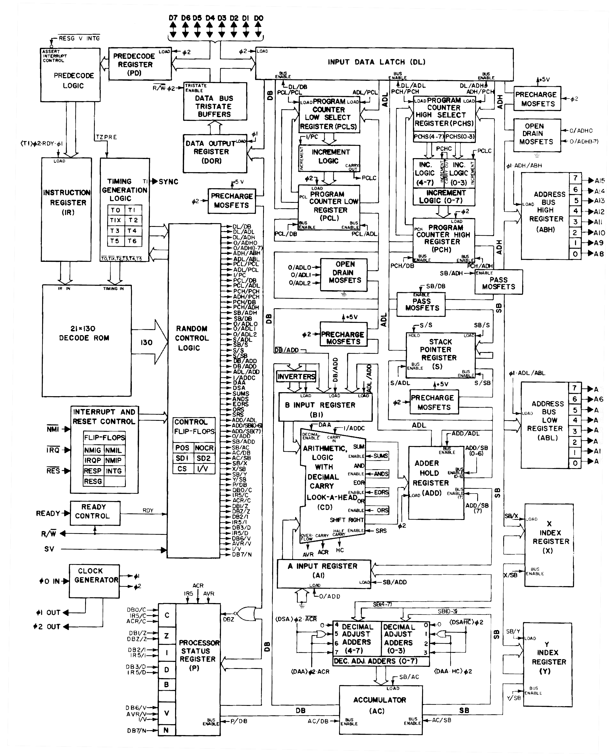
The diagram below (from the 8086 patent) shows how the ALU is connected to the rest of the processor by the ALU bus. The discussion above covered the "Full Function ALU" in the middle of the diagram, which takes two 16-bit inputs and produces a 16-bit output. These inputs are supplied from three temporary registers: A, B, and C. (These temporary registers are invisible to the programmer and should not be confused with the 8086's AX, BX, and CX registers.) I'll mention a few features of these registers that will be important later. Any register can provide the ALU's first input, but the second input always comes from the B register. These registers have a bidirectional connection to the ALU bus, so they can be both written and read. One unusual feature of the ALU is that it has a single data connection to the rest of the 8086, through the ALU bus.12 This seems like a bottleneck, since two clock cycles are required to load the registers, followed by another clock cycle to access the result. But apparently the single bus worked well enough for the 8086.

The Processor Status Word (PSW) shown above holds the condition flags, status bits on the ALU result: zero, negative, overflow, and so forth. Although the PSW looks trivial in the diagram above, the die photo at the top of the article shows that it constitutes about a third of the ALU circuitry. I'll leave the flag circuitry for a later discussion due to its complexity: each flag has unique circuitry that handles many special cases.
The schematic below shows one bit of the reverse-engineered implementation of the ALU's temporary registers. The registers are implemented with latches; each box represents a latch, a circuit that holds one bit. The two large AND-NOR gates act as multiplexers, selecting the output from one of the latches. The upper gate selects one of the registers for reading. The lower gate selects one of the registers as an argument for the ALU.

While the 6-input AND-NOR gate multiplexer may look complex, it is straightforward to implement with NMOS transistors. The schematic shows how it is built from 6 transistors and a pull-up. You can verify that if both transistors in a pair are energized, the output will be pulled to ground, providing the AND-NOR function.

The latch circuit is shown below. I've written about the 8086's latches in detail, so I'll give just a quick summary. The idea of the latch is that it can stably hold either a 0 or a 1 bit. When the clock signal clk' is high, the upper transistor is on, connecting the inverters into a loop. If the input to the first inverter is 1, it outputs a 0 to the second inverter, which outputs a 1 to the first, so they stay in that state, storing the bit. Similarly, the loop is stable if the input is a 0.

The special thing about this latch is that it's a dynamic latch. When the clock signal clk' is low, the loop is broken, but the input on the first inverter remains, due to the capacitance of the wire and transistor. When clk' goes high again, this voltage is refreshed. Alternatively, when clk' is low, a new value can be loaded into the latch by activating load, turning on the first transistor and allowing a new input signal to pass into the latch. The 8086 uses dynamic latches because the latch is compact, using just two transistors and two inverters. The latch is implemented in silicon as shown below.

The diagram below summarizes the components of the temporary register implementation. This circuitry is repeated 16 times to complete the registers.13 The output from the registers is fed into the ALU circuitry described earlier.

Conclusions
Although the Intel 8086 has complex circuits, its features are large enough that it can be studied under a microscope. The ALU is a key part of the processor and takes up a large fraction of the die. Its circuitry can be reverse-engineered through careful examination, revealing its interesting construction. It uses a Manchester carry chain for fast carry propagation. The carry-generate and carry-propagate signals are created by multiplexers that operate as arbitrary function generators, creating a flexible ALU with a small amount of circuitry. The ALU is built from a combination of standard logic, pass-transistor logic, and dynamic logic to optimize performance and minimize size.
You might have noticed that the 8086's ALU doesn't have support for multiplication, division, or multiple-bit shifts, even though the 8086 has instructions for these operations. These operations are computed in microcode using simpler ALU operations (shift, add, subtract for multiplication and division, and repeated single-bit shifts for larger shifts).
Some features of the ALU remain to be described, in particular the condition flags and how the ALU control signals are generated from opcodes. I plan to write about these soon, so follow me on Twitter @kenshirriff or RSS for updates.
Notes and references
-
The ALU size almost always matches the processor word size, but there are exceptions. Notably, the Z-80 is an 8-bit processor but has a 4-bit ALU. As a result, the Z-80's ALU runs twice for each arithmetic operation, processing half the byte at a time. Some early computers used a 1-bit ALU to keep costs down, but these serial processors were slow. ↩
-
I've looked at the ALU of various other early microprocessors including the 8008, Z-80, and the 8085. I've also reverse-engineered the 74181 and Am2901 ALU chips. ↩
-
The ALU's layout has bits 15-8 in the top and bits 7-0 below. This layout is a consequence of the bit ordering in the data path: the bits are interleaved 15-7-14-6-...-8-0, instead of linearly 15-14-...-0. The reason behind this interleaving is that it makes it easy to swap the two bytes in the 16-bit word, by swapping pairs of bits. The ALU is split into two rows so it fits into the horizontal space available. Even with the tall, narrow layout of an ALU stage, a bit of the ALU is wider than a bit of the register file. Splitting the ALU into two rows keeps the bit spacing approximately the same, avoiding long wires between the register file and the ALU. ↩
-
The Manchester carry chain was developed by the University of Manchester and described in the article Parallel addition in digital computers: a new fast 'carry' circuit, 1959. It was used in the Atlas supercomputer (1962). ↩
-
The ALU also uses carry-skip techniques to speed up carry calculation; I'll briefly summarize. The idea of carry-skip is to skip over some of the stages in the carry chain if possible, reducing the worst-case delay through the chain. For example, if there is a carry-in to bit 8, and the carry-propagate is set for bits 8, 9, 10, and 11, then it can be immediately determined that there is a carry-in to bit 12. Thus, by ANDing together the carry-in and the four carry-propagate values, the carry-in to bit 12 can be calculated immediately for this case. In other words, the carry skips from bit 8 to bit 12. Likewise, similar carry-skip circuits allow the carry to skip from bit 2 to bit 4, and bit 4 to bit 8. These carry-skip circuits reduced the ALU's worst-case computation time. The carry-skip circuitry explains why each stage in the ALU is similar but not quite identical. Note that for logic operations or shift, either carry-propagate or carry-generate is 0, so the carry-skip won't activate and corrupt the result. ↩
-
I should mention how subtraction is handled. A typical ALU inverts one of the inputs before adding, reusing the addition circuitry for subtraction. However, the 8086's ALU implements subtraction by changing the inputs to the multiplexers, as shown below. This leverages the general-purpose multiplexer and avoids implementing separate negation circuitry. (The comparison operation is implemented as subtraction but without storing the result. If the difference is zero, the values are equal, while a positive difference indicates the first value is larger.)
 Subtraction is similar to addition, but with the second argument negated. This is accomplished by inverting one input of the carry-generate AND gate and changing the carry-propagate XOR to XNOR.
 -
The typical way a processor implements a left shift by one bit is by adding the value to itself. I don't know why the 8086 used the carry approach rather than the adding approach. ↩
-
An FPGA (field-programmable gate array) uses similar techniques to implement arbitrary logic functions. The truth table is stored in a lookup table (LUT). These lookup tables are typically larger; a 6-input lookup table has 26 = 64 entries. One difference between the FPGA and the ALU is that the FPGA is programmed and then the gate functions are fixed, while the ALU's gates can change functions every operation. ↩
-
The carry-generate multiplexer returns 0 if argument 1 is 0. In other words, it only implements two cases of the truth table and has two control inputs. To handle the other two cases, it is pulled low by the clock signal so it outputs 0. Because it is driven by the clock and depends on the value held by the circuit capacitance, it is a form of dynamic logic. The 8086 primarily uses standard static logic, but uses dynamic logic in some places. ↩
-
The control signals for the ALU are generated from a PLA (similar to a ROM) that takes a 5-bit opcode as input. This opcode can either come from the instruction or be specified by the microcode. For an instruction, the ALU portion of the instruction is typically bits 5-3 of the first byte of the instruction or bits 5-3 of the MOD R/M byte. The point of this is that one microcode routine can handle all the similar arithmetic/logic instructions, making the microcode smaller. The ALU control PLA generates the signals to perform the correct ALU operation, transparently to the microcode. I should mention that there are many more ALU control signals than I described. Many of these control the flag handling, while others control various special cases.
The control signals pass through the peculiar circuit below. If the input is high, it sends a clock pulse to the ALU. Otherwise, it remains low. The drive signal is discharged to ground on the negative clock phase by the lower transistor. In the absence of an input, the signal is not driven during the positive clock phase, but remains low due to dynamic capacitance. One mystery is the transistor with its gate tied to +5V, leaving it permanently on, which seems pointless. It will reduce the voltage to the gate of the clk transistor, and thus the output voltage, but I don't see why. Maybe to reduce current? To slow the signal?
 The drive signals to the ALU gates are generated with this dynamic circuit.
 -
The pull-up resistor in an NMOS gate is implemented by a special depletion-mode transistor. The depletion-mode transistor acts as a resistor but is more compact and performs better than an actual resistor. ↩
-
In the 6502, the two inputs of the ALU are connected to separate buses (details), so they can both be loaded at the same time. The 8085 (and many other early microprocessors) connect the accumulator register to one input of the ALU to avoid use of the bus (details). ↩
-
The silicon implementation of the lower eight bits of the ALU / registers is flipped compared to the upper eight bits. The motivation is to put the ALU signals next to the flag circuitry that needs these signals. Since the flag circuitry is sandwiched between the two halves of the ALU, the two halves become (approximate) mirror images. (See the die photo at the top of the article.) ↩


7 comments:
About the shifting: add-to-self could only be applied to B, whereas the left-shift-using-carry could be applied to any of A, B and C. Possibly this, together with having as many as 3 temporary registers, is useful for multiplication.
Interesting point, Ed. I haven't figured out how multiplication works yet, so that's quite possible.
Another great article.
It's interesting that Mostek's effort to reverse engineer the 8086 under license failed and was stopped in 1981, if my memory is accurate. I only knew the project existed and was cancelled, nothing else, other than they had a license from Intel. It seems to me that your work shows that static logic would have been easy to duplicate, but the extensive use of dynamic logic might depend on both the process and layout. I noticed that the minimum clock rate is spec'ed at 500ns, I assume from the dynamic logic.
Comment on your Notes and references 1.
Digital Equipment’s PDP-8/S was designed as a cheap and cheerful low-end follow-up to the original, highly successful, PDP-8. The problem was that, to make it cheap, they had to make it bit-serial. The PDP-8 architecture is 12-bit - all operations are performed on 12-bit words. Normally that would mean that the hardware - accumulator etc. - was 12 bits wide. The 8/S however performs its 12 bit operations *one bit at a time* - hence 'bit-serial'. DEC sacrificed 12-bit parallel hardware to make it cheap. As a result it was crushingly slow, and sold very poorly.
Hi Ken,
Many thanks for this comprehensive article explaining FPGA, it solves quite some puzzles for me.
Still one question, what does configuration memory control? 8-pin switch matrix, programmable interconnection points, or both?
Thanks.
The outputs of B register's latch bit are connected differently (or swapped) to next stage (multiplexer). Is it like that only or there's error?
Anyway big fan of yours :D
Thanks for sharing, learnt a new circuit called Manchester carry chain and successfully find and download the patent file which helps me "randomly" guessing the logic of 8086 a lot.
Post a Comment